A microscopia de varredura por condutância iônica (SICM) usa correntes iônicas para imagens topográficas para estudar detalhes da superfície em células vivas. A microscopia de condutância iônica (SICM) usa correntes iônicas para gerar imagens topográficas e estudar detalhadamente a superfície das células vivas. Finalmente, o desempenho do microscópio desenvolvido foi testado para um novo modo de operação - Sensitive Backstep Hopping Mode.
Fundamental Concepts | Chapter 2 provides the relevant overview regarding the bases of SICM for the development process. Electrodynamics system | Chapter 5 presents the electrochemical system, including the manufacturing process for the electrodes and pipettes; as well as characterization of the resulting approach curves. Control System | Chapter 6 presents the control system, including the hardware communication, acquisition software, and piezoelectric stage characteristics.
Theory Overview and Framework
- Scanning Probe Microscopy
- Scanning Ion Conductance Microscopy
- Principle and Theoretical Modeling
- Imaging Modes
- a. Constant Z mode
- b. DC mode
- c. AC mode
- d. Hopping mode
- Imaging Techniques and Applications
- a. High Resolution Topography
- b. Smart Patch-Clamp
- c. Mechanical Stimulation
- d. Localized Delivery and Sampling
- e. SICM-SECM with a ring electrode or double barrel probe
- f. Scanning Electrochemical Cell Microscopy (SECCM)
- g. Potentiometric SICM (P-SICM)
- Advantages over Conventional Microscopies
The force acting between the sample surface and the tip causes the deflection of the cantilever and can be detected by an optical system. The topography is then constructed by measuring the relative z-position of the piezo actuator holding the pipette. As with DC mode, the pipette opening size also determines the image resolution.
![Table 1. SPM techniques and respective properties [7].](https://thumb-eu.123doks.com/thumbv2/123dok_br/19768857.0/19.892.110.771.337.809/table-1-spm-techniques-and-respective-properties-7.webp)
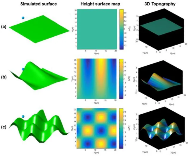
Modeling and Simulations
- Pipette inner radius estimation
- Approach curve estimation
- SICM scanning mode simulation
Far from the surface, the pipette access resistance in equation 5 is approximately constant, and according to James E. 4𝑟𝑖 (7) where ρ is the resistivity inverse to the conductivity (1/ 𝜅), of our bath solution 𝑟𝑖 is the radius of the opening of the pipette tip was intended to be predicted with this program. Once predicted, the approach curve of a given pipette can be used to draw conclusions about the sensitivity of the pipette.
The sensitivity directly depends on the inner radius 𝑟𝑖, which plays a key role in image quality and also depends on the shape of the pipette. The above equation was used to model this flow curve and the predicted curve as a function of pipette displacement can be compared to the actual approach curve. By comparing the measured current with the simulated case, it can be concluded that this model predicts approach curves similar to the actual case, again showing that this simulation is a useful and accurate tool for judging pipette quality and appropriate pipette sensitivity.
For this first batch, looking at the approach curve, we conclude that the pipette sensitivity is extremely poor and that these pipettes cannot be used to obtain images in the nm range. In this case, only the DC mode was implemented, based on a feedback loop to control the pipette position according to the current measurements, depending on the surface distance. By accessing the inner/outer pipette of the first batch manufactured using SEM, an approach curve was simulated and then compared to a real approach curve of a pipette taken from the batch.
After that, by pressing the DC button, the pipette represented by the blue blob starts to move pixel by pixel and the position is recorded.
SICM Construction
- SICM Design
- Nanopipette holder design
- SICM control support design
- SICM platform design
- SICM Manufacturing and Assembly
- Nanopipette holder manufacture
- SICM control support construction
- SICM platform construction
- SICM final setup assembly
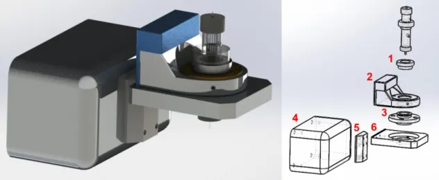
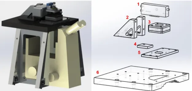
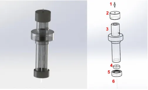
The first step in SICM construction involves the design of the nanopipette holder (Figure 17), then the main SICM head (Figure 18) and the main SICM platform (Figure 19). The pipette holder is shown in Figure 17 and consists of a long tube (3) (see Appendix B2), a top cap (2) (see Appendix B1) with a metal adapter (1) connecting the cable from the amplifier to the internal electrode through the tube in a nanopipette (6). The SICM control bracket containing the nanopipette holder is attached to the platform main table (6) (see Appendix B13) by means of 2 triangular brackets (2) (see Appendix B8 and B9).
The main function of this SICM element is to support Z-axis Piezo Actuator MIPOS 100, in Figure 21, connected to the nanopipette holder by an adapter (1). The function of the main head in Figure 21A is the displacement in the Z-range of the nanopipette, since the drive range of the Z-piezo is 100µm. To read the signal, a current amplifier DLPCA-200 (Figure 23.1) is used, which is placed in the main platform supported by a small piece (4).
Here is an image of the pipette holder and main head assembly. The SICM control stand containing the nanopipette holder is placed on the platform main board (Figure 24), after all the board components have been assembled as seen in Figure 24. Here is an image of the board assembly fitting the SICM to the optical microscope. upside down.
Here is a picture of the assembly of the pipette holder, main head and table.
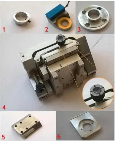
Electrochemical system
- Electrodes
- Nanopipettes manufacturing
- Approach Curves characterization
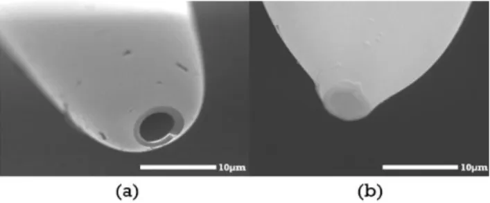
One of the electrodes connects to the ground and the other to the plug in the top cap, through the tube into the nanopipette. Here we show the response in current as a function of the applied voltage, tested in free bulk solution of 0.1 M HCl and inside the nanopipette. For other pipettes, an approach curve was not successfully obtained, even reading a current, which means that the tip opening is not perpendicular to the vertical axis of the pipette.
In Figure 35B it is possible to see the profile of the pipette walls (the tip looks blurred due to optical distortion). After production, the pipette must be mounted in the adapter before starting a new measurement (Figure 36C). For this purpose, the pipette is glued into the adapter and placed in a Teflon mold (Figure 36B).
Because we do it by hand and we don't have good sensitivity and the pipette breaks. However, sometimes no approach curve (or a distorted one) is achieved because the pipette shape is not good, so the pipette breaks very easily. In Figure 40 we show a typical approach curve, when the pipette approaches the surface at 1 Hz.
The probe moves step by step (typically 1 nm per step) and the current is read until a defined set point is reached, in this case 98% of maximum current.

Control System
- Main Control System
- Piezoelectric stages
- Acquisition Software
- Real time interface
- a. Approach to the surface
- b. Approach curve characterization
- c. Scanning
- d. Data Processing
- FPGA interface
In the closed loop system, a PID reads the actual position of a sensor and corrects the signal to the setpoint coming from the controller, correcting non-linearities in real time, as shown in Figure 43b. The acquisition software is implemented in LabVIEW Real-time based programming and compiled into the computer. The code can be seen in appendix F. By clicking on the hopping approach at the bottom (yellow bottom top left) we automatically approach the surface, covering a distance of 100 µm.
If the current decrease is not detected, the user stops the jump by clicking the stop bottom (red bottom top left) and the holder head is manually approached to a distance of 80 µm. The program is mainly divided into surface approach (left), surface scanning (middle) and image processing (right). For an effective approach, the parameters must be correctly set, the approach speed ("Z Rate [µm]"), the displacement ("displacement step [µm]"), the Z piezo sensitivity ("Zpiezo Sense [V /µm]") and the set value ( “Setpoint Voltage [mV]”).
Then, on each turn, a while loop sends the position to the piezo via the FPGA (at the previously defined approach speed). Meanwhile, the current is read and plotted in the Real-time Acquisition graph at the top left of Figure 45. If the current drops by the defined set point, the loop is interrupted. The position (“position [μm]”) and the current signal (“signal [V]”) are displayed on the screen in real time, and the position where the setpoint is reached (“Setpoint position [μm]”) is then displayed every approach curve (theoretically should be the same for the same position if the system is well shielded from the noise and the set point chosen is appropriate for the pipette size).
The user can then select the scan mode on the separator and set the relevant mode parameters before the scan starts.

Imaging Performance
- DC Mode
- Implementation
- DC Scanning
- Sensitive Backstep hopping mode (SBH mode)
- Implementation
- Backstep Scanning
The slope of the surface follows the movement of the pipette over the XY phase displacement shown in Figure 44. These four images show XtraceYtrace, XtraceYtrace, XtraceYretrace and XretraceYretrace according to the xy piezo displacement shown in Figure 44. As the main program and new scan mode, u implemented background jump mode.
Similarly, the traditional hop mode (Figure 52) lowers the probe towards the sample until the given set point is reached, and the height is recorded, but in SBH mode the probe is lowered more slowly near the surface, which shows the drop in current more accurately detected. Then the pipette is moved laterally and another measurement is taken, and the process is repeated until the sample topography is reconstructed. Apparently, we have a flatter baseline and better tracking for this scan mode, compared to the traditional hoop mode performance shown in Figure 40.
The figure below shows the low-resolution topography of the smaller line in Figure 54d and the larger line in Figure 54b with the respective elevation profile in Figure 54c. The calibration sample sizes were characterized by a profilometer and the image under an optical microscope is shown in A, D shows the topography of the smaller line and the 3D can be seen in E. The figure below shows the SICM topography (Figure 55b) corresponding with the profile expected from optical microscopy.
A higher-resolution scan of the stretched ribbon in A and a lower-resolution scan in B highlighting the filaments connecting the spots.

For this we need to set the resistance of the pipette 𝑅𝑝 in Mohm, the conductivity of the medium 𝜅 in mS and the angle between the central axis of the pipette and its walls theta (𝜃) in degrees. For this we need to set the voltage used to connect the electrodes V in mV, the resistance of the pipette 𝑅𝑝 in MOhm, the conductivity of the medium 𝜅 in mS, the angle between the central axis of the pipette and its walls theta (𝜃) in degrees and the outer/inner radius (𝑟𝑜 and 𝑟𝑖) in µm. Scan Size panel: Contains the parameters to be set before scanning, XX and YY represent the image size in µm, the sampling rate in Hz and the set point in percentage.
Start mode panel: Contains a scan of the mode to be simulated, and the next panel, Abort, contains the control buttons. The orange sphere corresponds to the position of the pipette opening and the resulting topography is drawn in the center. In addition, the pipette resistance 𝑅𝑝, peak current 𝐼𝑠𝑎𝑡 and set point current 𝐼𝑠𝑎𝑡, resolution and height of the pipette at each position can be accessed from this panel.
Simultaneous measurement of Ca2+ and cellular dynamics: combined ion scanning conductance and optical microscopy to study contracting cardiac myocytes, Elsevier, Biophys. Korchev (2008), Noninvasive imaging of stem cells by scanning ion conduction microscopy: future perspectives, India India: Part C Methods 14, 311. Scanning ion conduction microscopy: a convergent high-resolution technology for multi-parametric analysis of cardiovascular living cells, J.
Localized and non-contact mechanical stimulation of sensory neurons of the dorsal root ganglion using scanning ion conduction microscopy, J. Imaging the surface of living cells by low-power atomic force microscopy in contact mode. High-resolution AFM of membrane proteins recorded directly at high density in planar lipid bilayer.

![Figure 7 | Imaging techniques in SICM [18]. The most common technique in SICM is high resolution topography and its combination with Fluorescence microscopy (b), however this microscopy can also be adapted to specific techniques, like sma](https://thumb-eu.123doks.com/thumbv2/123dok_br/19768857.0/26.892.110.746.392.803/techniques-resolution-topography-combination-fluorescence-microscopy-microscopy-techniques.webp)
![Figure 10 | Observable Pressure Range of SICM and AFM for Various Cell Types [55].](https://thumb-eu.123doks.com/thumbv2/123dok_br/19768857.0/31.892.185.704.104.401/figure-observable-pressure-range-sicm-various-cell-types.webp)
![Figure 9 | Complex features on cell membrane [55]. The cellular membrane is very complex, composed by a rigid and stiff cytoskeleton, fluidic lipid bilayer, and small and delicate features](https://thumb-eu.123doks.com/thumbv2/123dok_br/19768857.0/31.892.208.681.686.986/complex-features-membrane-cellular-membrane-composed-cytoskeleton-delicate.webp)