PRELIMINAR
1 ESPRISCV CPU
Overview
Features
Address Map
Configuration and Status Registers (CSRs)
- Register Summary
- Register Description
This is automatically updated with the address of the command that should have been executed while the CPU encountered the last trap. Exception Code This field is automatically updated with the unique ID of the last exception or interrupt that caused the CPU to enter the trap.
Interrupt Controller
- Features
- Functional Description
- Suggested Operation .1 Latency Aspects
- Configuration Procedure
- Register Summary
- Register Description
Steady state means that no recent changes have been made to the interrupt controller registers. After executing the sequence above, the interrupt controller will resume steady state operation.

Debug
- Overview
- Features
- Functional Description
- Register Summary
- Register Description
If the instruction does not complete due to an exception, the core will immediately enter Debug mode before executing the trap handler, with the appropriate exception registers set. A debugger can change this value to change the kernel's privilege level when exiting Debug Mode.
Hardware Trigger
- Features
- Functional Description
- Trigger Execution Flow
- Register Summary
- Register Description
This will always be interpreted as an address, as only match type triggers (0x2) are supported. mpte Enable bit of previous enable of machine mode. Set this to configure the selected trigger to fire immediately before an instruction with a matching virtual address is executed by the CPU. store Set this to configure the selected trigger to fire immediately before a store operation with the matching data address is executed by the CPU.
Memory Protection
- Overview
- Features
- Functional Description
- Register Summary
- Register Description
Overview
Features
Architecture
Functional Description
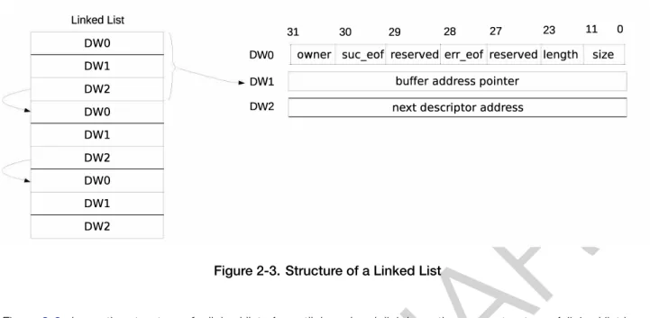
- Linked List
- PeripheraltoMemory and MemorytoPeripheral Data Transfer
- MemorytoMemory Data Transfer
- Enabling GDMA
- Linked List Reading Process
- Accessing Internal RAM
- Arbitration
- Bandwidth
The GDMA controller can transfer data from memory to peripheral (send) and from peripheral to memory (receive). Before the GDMA controller receives data, GDMA_IN_SUC_EOF_CHn_INT_ENAbit must be set to enable GDMA_IN_SUC_EOF_CHn_INT interrupt.
GDMA Interrupts
GDMA_IN_SUC_EOF_CHn_INT: Triggered when a data packet has been received over the receive channel. GDMA_IN_DONE_CHn_INT: Triggered when all data corresponding to the receive descriptor has been received over the receive channel.
Programming Procedures
- Programming Procedures for GDMA’s Transmit Channel
- Programming Procedures for GDMA’s Receive Channel
- Programming Procedures for MemorytoMemory Transfer
GDMA_OUT_DONE_CHn_INT: Activated when all data corresponding to a transmission descriptor has been sent over the transmission channel. GDMA_IN_ERR_EOF_CHn_INT: Triggered when an error is detected in the data packet received via the received channel.
Register Summary
EOF Occurs for TX Channel 0 0x00EC RO GDMA_OUT_DSCR_CH0_REG Current inlink descriptor address for TX. EOF Occurs for TX Channel 2 0x026C RO GDMA_OUT_DSCR_CH2_REG Current inlink descriptor address for TX.
Registers
GDMA_IN_DSCR_ERR_CH0_INT_ST. GDMA_OUT_EOF_CH0_INT_ST. GDMA_OUT_DONE_CH0_INT_ST. GDMA_IN_ERR_EOF_CH0_INT_ST. GDMA_IN_SUC_EOF_CH0_INT_ST. GDMA_IN_DONE_CH0_INT_ST. GDMA_INLINK_DSCR_BF1_CHn Naslov predzadnjega deskriptorja povezave x-2. GDMA_OUT_REMAIN_UNDER_4B_CH0.
Overview
Features
The range of available addresses in the address space can be larger than the actual available memory of a particular type.
Functional Description
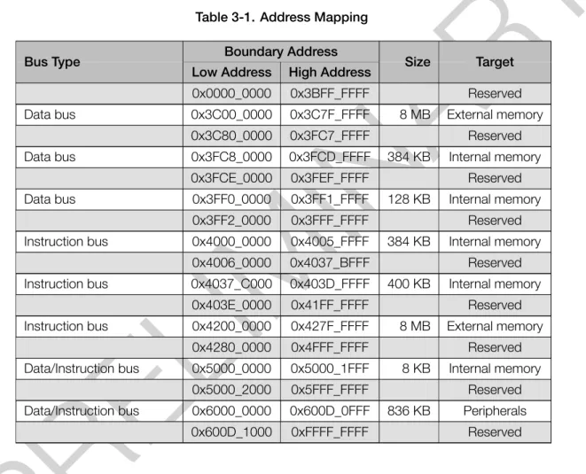
- Address Mapping
- Internal Memory
- External Memory
- External Memory Address Mapping
- Cache
- Cache Operations
- GDMA Address Space
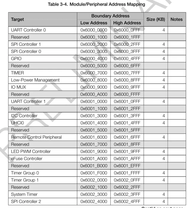
- Modules/Peripherals
- Module/Peripheral Address Mapping
Table 3-2 describes each part of the internal memory and their address ranges on the data bus and/or the instruction bus. Table 3-3 shows the mapping between the cache and the corresponding address areas on the data bus and the instruction bus. Once this operation is completed, the data will only be stored in the external memory.
Overview
Features
Functional Description
- Structure
- EFUSE_WR_DIS
- EFUSE_RD_DIS
- Data Storage
- Software Programming of Parameters
- Software Reading of Parameters
- eFuse VDDQ Timing
- The Use of Parameters by Hardware Modules
- Interrupts
RegisterEFUSE_PGM_DATA1_REG~EFUSE_PGM_DATA5_REG stores the information about parameters to be programmed. EFUSE_PGM_DATA0_REG~EFUSE_PGM_DATA7_REGsave the parameters to be programmed for this block. RegisterEFUSE_PGM_CHECK_VALUE0_REG~EFUSE_PGM_CHECK_VALUE2_REG stores the corresponding RS check codes.

Register Summary
EFUSE_CLK_REG eFuse Clock Configuration Register 0x01C8 R/W EFUSE_CONF_REG eFuse Operating Mode Configuration Register 0x01CC R/W. EFUSE_DAC_CONF_REG Controls the eFuse programming voltage 0x01E8 R/W EFUSE_RD_TIM_CONF_REG Configures read time parameters 0x01EC R/W EFUSE_WR_TIM_CONF1_REG Configuration register 1 for eFuse programming. EFUSE_INT_RAW_REG eFuse Raw Interrupt Register 0x01D8 R/WC/SS EFUSE_INT_ST_REG eFuse Interrupt Status Register 0x01DC RO.
Registers
EFUSE_SYS_DATA_PART2_7 Stores the 7th 32 bits of the 2nd part of system data. EFUSE_VDD_SPI_AS_GPIO_ERR. EFUSE_USB_EXCHG_PINS_ERR. EFUSE_DIS_FORCE_DOWNLOAD_ERR. EFUSE_DIS_USB_SERIAL_JT AG_ERR. EFUSE_DIS_DOWNLOAD_ICACHE_ERR. EFUSE_DIS_USB_JT AG_ERR. RO) EFUSE_KEY5_FAIL 0: Means no failure and that the data of KEY5 is reliable 1: Means that program-. ming KEY5 data failed and the number of error bytes is more than 6. EFUSE_EFUSE_MEM_FORCE_PU.
EFUSE_PGM_DONE_INT_RA W. EFUSE_READ_DONE_INT_RA W. EFUSE_READ_DONE_INT_RAW Raw bit signal for read_done interrupt. R/WC/SS) EFUSE_PGM_DONE_INT_RAW Raw bit signal for pgm_done interrupt. EFUSE_PGM_DONE_INT_ST.
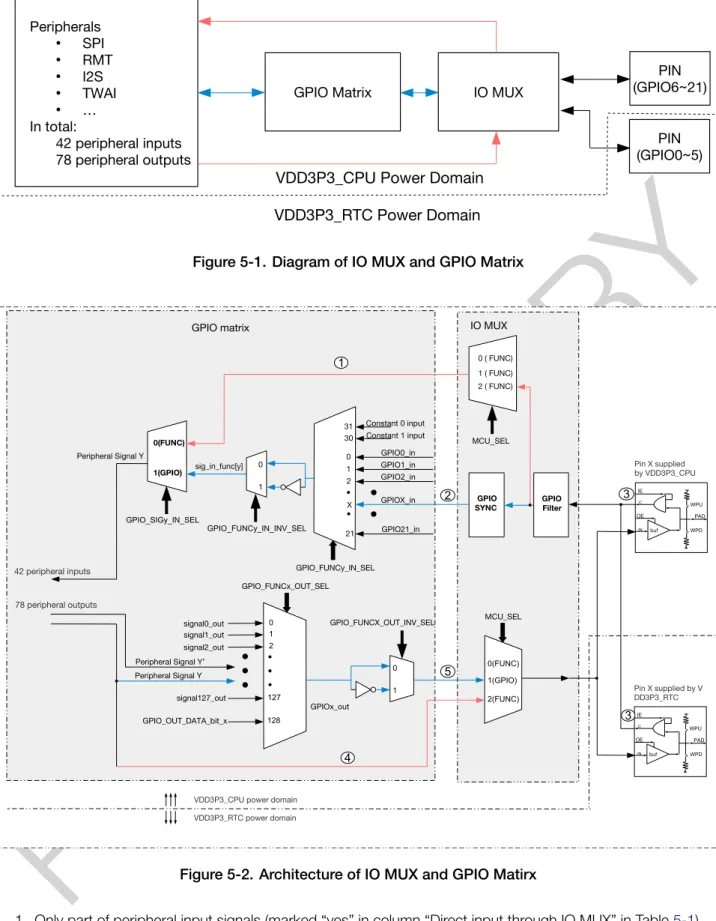
Overview
Features
Architectural Overview
Only some of the peripheral input signals (marked “yes” in the “Direct input via IO MUX” column in Table 5-1) can bypass the GPIO matrix. Only some of the peripheral outputs (marked “yes” in the “Direct Output via IO MUX” column in Table 5-1) can do that. Figure 5-3 shows the internal structure of a pad, an electrical interface between the chip logic and the GPIO pin.
Peripheral Input via GPIO Matrix
- Overview
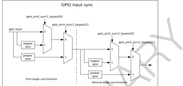
- Signal Synchronization
- Functional Description
- Simple GPIO Input
Note that some peripherals do not have GPIO_SIGy_IN_SELbit valid, that is, these peripherals can only receive input signals via the GPIO matrix. Set GPIO_SIG12_IN_SEL to the GPIO_FUNC12_IN_SEL_CFG_REG register to enable peripheral signal input via the GPIO matrix. The input value of any GPIO pin can be read at any time without configuring the GPIO matrix for a specific peripheral signal.
Peripheral Output via GPIO Matrix
- Overview
- Functional Description
- Simple GPIO Output
- Sigma Delta Modulated Output (SDM) .1 Functional Description
- SDM Configuration
Optionally set or clear IO_MUX_GPIOx_FUN_WPU and IO_MUX_GPIOx_FUN_WPD to enable or disable pull-up and pull-up resistors. However, input via the IO MUX must be enabled by setting the IO_MUX_GPIOx_FUN_IEbit in the IO_MUX_GPIOx_REG register corresponding to the pinX as mentioned in section 5.4.2. Set the IO_MUX_GPIOx_MCU_SEL field to the desired IO MUX function corresponding to the GPIO pinX.
Direct Input and Output via IO MUX
- Overview
- Functional Description
For PDM signals, the duty cycle refers to the percentage of high-level cycles relative to the total statistical period (multiple pulse cycles, for example 256 pulse cycles).
Analog Functions of GPIO Pins
Pin Hold Feature
Power Supplies and Management of GPIO Pins
- Power Supplies of GPIO Pins
- Power Supply Management
Peripheral Signal List
Only the signals with a name assigned in the "Input Signal" column in Table5-1 are valid input signals. Only the signals with a name assigned in the "Output Signal" column in Table 5-1 are valid output signals.
IO MUX Functions List
The USB pull-up value of GPIO19 is 1 by default, therefore, the pin pull-up resistor is enabled. If any of the pull-up values is 1, the pin's pull-up resistor will be enabled. The pull-up resistors of the USB pins are controlled by USB_SERIAL_JTAG_DP_PULLUP.
Analog Functions List
If eFuse bit EFUSE_DIS_PAD_JTAG = 0, the MTCK pin is connected to an internal pull-up resistor, i.e.
Register Summary
- GPIO Matrix Register Summary
- IO MUX Register Summary
- SDM Register Summary
GPIO_FUNC0_IN_SEL_CFG_REG Configuration register for input signal 0 0x0154 R/W GPIO_FUNC1_IN_SEL_CFG_REG Configuration register for input signal 1 0x0158 R/W. GPIO_FUNC127_IN_SEL_CFG_REG Configuration register for input signal 127 0x0350 R/W Output Function Configuration registers. IO_MUX_PIN_CTRL_REG Clock Output Configuration Register 0x0000 R/W IO_MUX_GPIO0_REG IO MUX configuration register for pin.
Registers
- GPIO Matrix Registers
- IO MUX Registers
- SDM Output Registers
IO_MUX_GPIO5_REG IO MUX configuration register for pin MTDI 0x0018 R/W IO_MUX_GPIO6_REG IO MUX configuration register for pin MTCK 0x001C R/W IO_MUX_GPIO7_REG IO MUX configuration register for pin MTDO 0x0020 R/W IO_MUX_GPIO8_REG IO MUX configuration register for pin GPIO8 0 x0024 R/W IO_MUX_GPIO9_REG IO MUX configuration register for pin GPIO9 0x0028 R/W IO_MUX_GPIO10_REG IO MUX configuration register for pin GPIO10 0x002C R/W IO_MUX_GPIO11_REG IO MUX configuration register for pin VDD_SPI 0x0030 R/W IO_MUX_GPIO12_REG IO MUX configuration register for pin SPIHD 0x0034 R /W IO _MUX_GPIO13_REG IO MUX configuration register for pin SPIWP 0x0038 R/W IO_MUX_GPIO14_REG IO MUX configuration register for pin SPICS0 0x003C R/W IO_MUX_GPIO15_REG IO MUX configuration register for pin SPICLK 0x0040 R/W IO_MUX_GPIO16_REG IO MUX configuration register for pin SPID 0x0044 R/W IO_M UX_GPIO 17_REG IO MUX configuration register for pin SPIQ 0x0048 R/W IO_MUX_GPIO18_REG IO MUX configuration register for pin GPIO18 0x004C R/W IO_MUX_GPIO19_REG IO MUX configuration register for pin GPIO19 0x0050 R/W IO_MUX_GPIO20_REG IO MUX configuration register for pin U0RXD 0x0054 R/W IO _MUX _GPIO21_REG IO MUX configuration register for pin U0TXD 0x0058 R/ Register W version. The addresses in this section are relative to the IO MUX base address given in Table 3-4 in Chapter 3 System and Memory. IO_MUX_CLK_OUTx To output the clock for I2S to CLK_OUT_outx, set IO_MUX_CLK_OUTx to 0x0.
Reset
- Overview
- Architectural Overview
- Features
- Functional Description
System Reset Triggered by Brown Detector2 0x10 RWDT System Reset System Reset See Chapter 11Watchdog Timers (WDT) 0x12 Super Watchdog Reset System Reset See Chapter 11Watchdog Timers (WDT) 0x13 CLK GLITCH System Reset Reset See Chapter 20Clock Glitch Detection. 0x07 MWDT0 Core Reset Core Reset See Chapter 11Watchdog Timers (WDT) 0x08 MWDT1 Core Reset Core Reset See Chapter 11Watchdog Timers (WDT) 0x09 RWDT Core Reset Core Reset See Chapter 11Watchdog Timers (WDT) 0x14 eFuse Core Reset Trigger e CRC fuse error. 0x0C Software CPU Reset CPU Reset Trigger Configuration RTC_CNTL_SW_PROCPU_RST 0x0D RWDT CPU Reset CPU Reset See Chapter 11Watchdog Timers (WDT).
Clock
- Overview
- Architectural Overview
- Features
- Functional Description .1 CPU Clock
- Peripheral Clock
- WiFi and Bluetooth ® LE Clock
- RTC Clock
The frequency of APB_CLK is determined by the clock source of CPU_CLK as shown in Table6-5. The frequency of CRYPTO_CLK is determined by the CPU_CLK source, as shown in Table6-6. Wi-Fi and Bluetooth LE can only work when CPU_CLK uses PLL_CLK as its clock source.
Overview
Boot Mode Control
If this eFuse is 0 (default), software can force the chip from SPI Boot mode to download boot mode by setting the RTC_CNTL_FORCE_DOWNLOAD_BOOT register and causing a CPU reset. If this eFuse is 1, download boot mode only allows reading, writing, and erasing plaintext and does not support any SRAM or write operations. The USB Serial/JTAG controller can also force the chip into download boot mode from SPI Boot mode, as well as force the chip into SPI Boot mode from download boot mode.
ROM Code Printing Control
In Download Boot mode, users can download code to flash using the UART0 or USB interface. ROM code will be printed to the U0TXD pin (default) or to the USB Serial/JTAG controller during boot, depending on the eFuseEFUSE_USB_PRINT_CHANNEL(0: USB; 1: UART) bit. Note that if this eFuse bit is set to 0, i.e. USB is selected, but the USB Serial/JTAG Controller is disabled, then the ROM code will not be printed.
Overview
Features
Functional Description
- Peripheral Interrupt Sources
- CPU Interrupts
- Allocate Peripheral Interrupt Source to CPU Interrupt
- Allocate one peripheral interrupt source (Source_X) to CPU
- Allocate multiple peripheral interrupt sources (Source_Xn) to CPU
- Disable CPU peripheral interrupt source (Source_X)
- Query Current Interrupt Status of Peripheral Interrupt Source
55 DMA_APB_PMS_MONITOR_VIOLATE_INTR INTERRUPT_CORE0_DMA_APBPERI_PMS_MONITOR_VIOLATE_INTR_MAP_REG 23. 58 CORE_0_PIF_PMS_MONITOR_VIOLATE_INTR INTERRUPT_CORE0_CORE_0_PIF_PMS_MONITOR_VIOLATE_INTR_MAP_REG 2 6. INTERRUPT_CORE0_SOURCE_X_MAP_REG: pomeni konfiguracijski register za vir periferne prekinitve (Source_X).
Register Summary
INTERRUPT_CORE0_BACKUP_PMS_VIOLATE_INTR_MAP_REG BACKUP_PMS_VIOLATE Map Register 0x00F0 R/W INTERRUPT_CORE0_CACHE_CORE0_ACS_INT_MAP_REG CACHE_CORE0_ACS Map Register 0x00F4 R/W Interrupt Resource Status Register. INTERRUPT_CORE0_INTR_STATUS_0_REG Status register for interrupt resources 0~31 0x00F8 RO INTERRUPT_CORE0_INTR_STATUS_1_REG Status register for interrupt resources 32~61 0x00FC RO Clock register. INTERRUPT_CORE0_CPU_INT_ENABLE_REG Enable CPU Interrupt Register 0x0104 R/W INTERRUPT_CORE0_CPU_INT_TYPE_REG CPU Interrupt Configuration Register Type 0x0108 R/W.
Registers
INTERRUPT_CORE0_CPU_INT_ENABLE Writing 1 to the bit here enables the corresponding CPU interrupt. INTERRUPT_CORE0_CPU_INT_CLEAR Writing 1 to the bit here will clear the associated CPU interrupt.
Overview
Features
Clock Source Selection
Functional Description
- Counter
- Comparator and Alarm
- Synchronization Operation
- Interrupt
The lower 32 and higher 20 bits of the initial count value are loaded from the SYSTIMER_TIMER_UNITn_LOAD registers. The lower 32 and higher 20 bits of the current count value are locked in the registersSYSTIMER_TIMER_UNITn_VALUE_LOand. Assuming the current count value is t2 (t2 <= t), an alarm interrupt is generated when the count value reaches the alarm value (t).
Programming Procedure
- Read Current Count Value