Critical components1 of the Semiconductor Group of Siemens AG may only be used in life-sustaining devices or systems2 with the express written permission of the Semiconductor Group of Siemens AG. Siemens Semiconductor's TriCore Instruction Set Architecture (ISA) combines the real-time performance of a microcontroller, the computing power of a DSP, and the high-performance/cost-effectiveness of a RISC load/store architecture in a compact unit. , a reprogrammable core. You can also choose the type and size of on-chip memory: SRAM, DRAM, ROM, Flash and OTP.
Large memory blocks on the chip (RAM, ROM, DRAM, OTP, FLASH) enable higher capacity, more reliable operation and reduced system energy consumption.
TriCore Instruction Categories
The architecture allows for a wide variety of implementations, ranging from simple scalar to superscalar. This flexibility at the deployment and system level allows different trade-offs between performance and cost at any given time. The architecture's native microcontroller DSP capabilities allow you to tune, via software, the microcontroller and DSP performance of each TriCore core.
For example, the performance of a 100 MHz TriCore-1 core with a sustained rating of 130 MIPS is 80 microcontroller MIPS + 50 DSP MI-PS, or 40 microcontroller MIPS + 90 DSP MIPS, depending on how the system designer implements the partitioning of the load. in software.
Target Applications
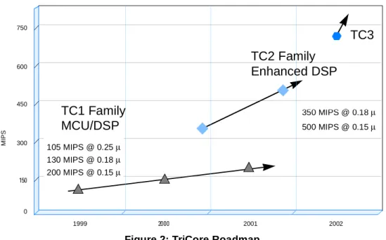
TriCore Roadmap
This section discusses the aspects of the TriCore architecture that are visible to software: the supported data types and formats, the different addressing modes that the architecture provides, and the memory model.
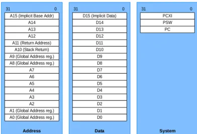
Architectural Registers
Data Types and Formats
Sign or zero extension is currently done as part of the load operation. The CPU's data memory and registers store data in little-endian byte order (the least significant bytes are at the lowest addresses). When the TriCore system is connected to an external big-endian device, the translation between big- and small-endian format is performed by the bus interface.
Addresses (32 bits) must be aligned on a word boundary to allow transfers between address registers and memory.
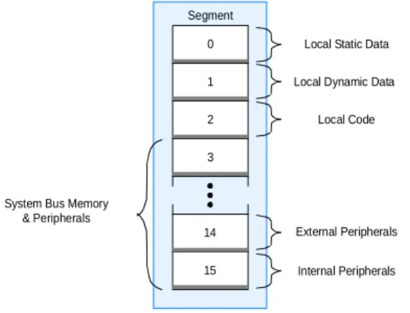
Memory Model
General purpose registers are all 32 bits wide and most instructions operate on word (32-bit) values. Thus, when data with fewer bits than a word is loaded from memory, it must be marked or zero-extended before operations can be applied to the full word. For transfers between data registers and memory, data can be aligned on any halfword boundary, regardless of size; bytes can be accessed at a valid byte address, with no extent restrictions.
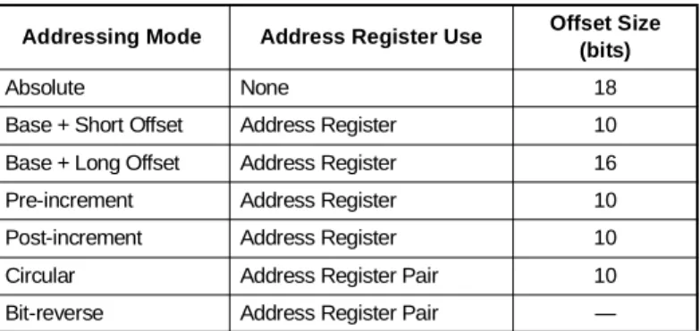
Addressing Modes
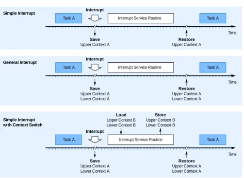
The upper context consists of the upper address registers, A10 - A15, and the upper data registers, D8 - D15. The TriCore architecture saves and restores the context much faster than conventional microprocessors and microcontrollers. Its unique memory subsystem design with a wide data path enables the TriCore architecture to perform fast data transfers between processor registers and on-chip memory.
For a simple interrupt, the TriCore automatically saves the upper context when the interrupt service routine (ISR) is entered. When the Return from Execution instruction is issued, the upper context is automatically restored from the time of the interrupt. Both upper and lower context registers can be used within the rest of the ISR.
Before returning to Task 1, the restore lower context instruction is issued, followed by an exception return, which automatically restores the upper context. The TriCore's security system provides the essential functions to isolate errors and facilitate debugging. The built-in architecture of the TriCore allows each task to be assigned the specific level of authority required to perform its function.
The memory protection model for the TriCore architecture is based on address ranges, where each address range has an associated permission setting. When the protection system is enabled, TriCore checks each load/store address or receiving instructions for legality before performing access.
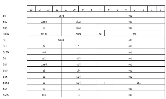
Instruction Set Summary
Complete information on all instructions can be found in Siemens Semiconductor's TriCore Architecture Manual. ABSDIF Absolute value of difference DVINIT Divide initialization word ABSDIFS Absolute value of difference with saturation DVSTEP Divide step. CACHEA.W Cache Address Writeback JGE Jump if greater than or equal to CACHEA.WI Cache Address Writeback and Invalidate JGEZ Jump if greater than or equal to.
MADDR(S).H Packed Multiply-Add Q Format w/ Rounding OR.comp Compare, OR and Accumulate MADDR(S).Q Multiply-Add Q Format w/ Rounding OR.logic Bit OR logic Accumulation MADDSU(S).H Packed Multiply-Add/sub Q Format ORN Logical OR not. MSUB(S) Multiply-Subtract (S = with saturation) SELN Select Not MSUBAD(S).H Packed Multiply-Sub/Add Q Format SH Shift MSUBADM(S).H Packed Multiply-Sub/Add Q Format - Multi-. TRAPSV Trap on sticky overflow XOR.comp Compare, XOR and accumulate XNOR Logic exclusive NOR.
Refer to the TriCore Architecture Manual for more information on instruction formats and their memory.
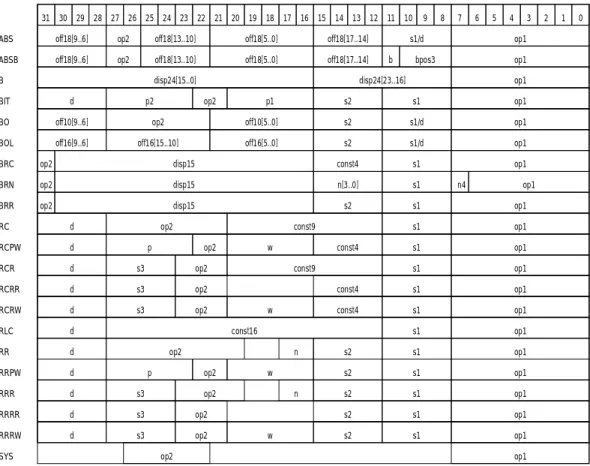
Load and Store Instructions
Multiplication of two 32-bit integers that produces a 32-bit result can be handled using MUL (Multiply Signed), MULS (Multiply Signed with Saturation), and MULS.U (Multiply Unsigned with Saturation). The MADD, MADDS (Multiply-Add with Saturation), and MADDS.U (Multiply-Add with Saturation Unsigned) instructions operate on and produce 32-bit integers; MADDS and MADDS.U will be saturated on signed and unsigned overflow respectively. The TriCore ISA supports division of 32-bit by 32-bit integers for both signed and unsigned integers through a divide-step sequence that reduces interrupt latency (the length of time interrupts must be disabled).
SAT instructions saturate the result of a 32-bit calculation before storing it in a byte or halfword in memory or a register. DSP arithmetic instructions operate on 16-bit signed fractional data in 1.15 format (also known as Q15) and 32-bit signed fractional data in 1.31 format (also known as Q31). Left-aligning 16-bit data allows it to be appended directly to 32-bit data in the 1.31 format.
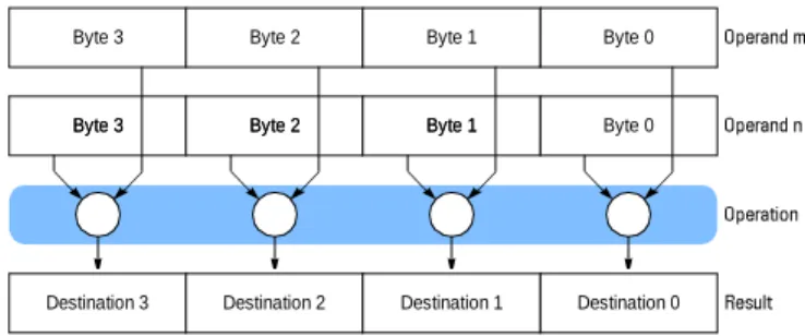
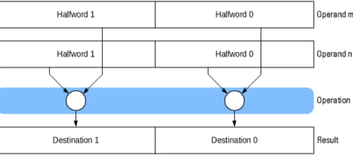
Rounding is combined with the MUL, MADD, MSUB instructions and implemented by adding 1 to bit 15 of a 32-bit register. Packed arithmetic instructions divide a 32-bit word into several identical objects, which can then be retrieved, stored, and operated on in parallel. These instructions, in particular, allow full utilization of the 32-bit word of the TriCore architecture in signal and data processing applications.
Instructions that operate on data in this way are indicated in the instruction mnemonic with the ".H" and ".HU" data type modifiers. Instructions that act on the data in this way are indicated by the ".B" and ".BU" data type modifiers.
Branch Instructions
System Instructions
According to your design requirements, you can easily add peripherals and memory modules to the basic model from the Siemens library. The core features an FPI bus interface for easy interfacing with all types of internal and external peripherals, memories, and various active bus agents such as CPUs, DMA/PCP controllers, and coprocessors. The following subsections discuss the core and optional modules that can make up a TriCore-1 chip.
TriCore-1 Core
FPI Bus Overview
Slave agents, which only support simple reading and writing of registers and do not actively operate on the bus protocol. Master-slave agents, which support advanced features such as support for split read transfer and error handling. Depending on the type of transaction, these agents can act as master or slave or both.
Peripheral Control Processor Module
This functionality can be used to handle many service operations required by peripherals that would normally be performed via the interrupt service routine via the CPU, with all the overhead involved. Change a bit or bit field in a peripheral register (eg start or stop a timer or A/D converter). Move data only if its value matches predefined limits (eg monitor specific voltage limits on analog inputs).
In addition, you can use the PCP to perform control operations on the CPU or peripherals. Calculation results of the CPU can be checked against predefined ranges using the DMA/PCP. The integrity of peripheral control registers can also be monitored by, for example, comparing their contents to a predetermined table stored in memory) using the PCP.
The service request unit performs the arbitration of the various sources' requests and provides service to the request that has the highest priority at a given time. The PCP channel control code can be stored locally to the PCP or to any memory accessible via the FPI bus.
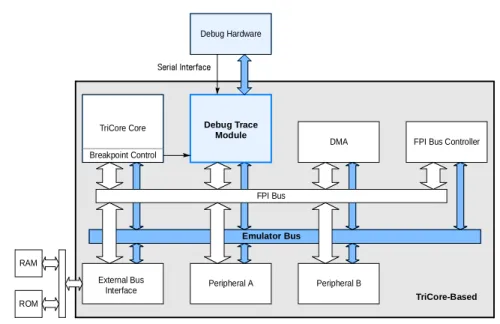
Debug/Emulation Module
The operation of the TriCore core, DMA and debug interface can be monitored in real-time via the TriCore real-time trace output. The TriCore architecture is well supported by a robust set of hardware and software development tools (see Figure 18). These tools include the TriCore Instruction Set Simulator (TSIM), a compiler-as-assembler debugging toolchain, real-time operating systems, and emulators.
The architecture of the instruction set was developed in close consultation with third-party providers of these tools. The TriCore instruction set simulator (TSIM) is bundled with complete toolchains (debugger-compiler-assembler-linker-loader) from several vendors. TSIM is a configurable, instruction-accurate model of the underlying TriCore-1 architecture that is built into all supported source-level debuggers.
You can reprogram the TriCore-1 core to evaluate your deployment approach by changing the memory parameters in the TSIM memory configuration (MConfig) file. You can also specify interrupt events in the TSIM interrupt configuration (IConfig) file to evaluate interrupt operation and performance. The TSIM peripheral configuration (PConfig) file tells your program how to communicate with the peripherals used in this implementation.
The core and modules are interconnected via the FPI bus, with up to 32 bits of address and 64 bits of data, and a maximum throughput of 800 Mbytes/s at 100 MHz. The debugging mechanism provides easy hardware-software integration through breakpoint support in the kernel, the debug port that provides access to the breakpoint, other system resources, and the real-time trace port. While the next two MACs are being performed, the first set of registers is loaded with the next 8 operands.
For us, this means meeting your every request in the best possible way.