ISSN 1546-9239
© 2006 Science Publications
Corresponding Author: Samia Pillai Pitchai, Department of Electrical and Electronics Engineering, College of Engineering, Anna University, Chennai 600 025. India
A Low Cost Design Solution - DSP Based Active Power Factor Corrector
for SMPS/ UPS( Single Phase)
Samia Pillai Pitchai and B.Umamaheswari
Department of Electrical and Electronics Engineering, College of Engineering, Anna University
Chennai 600 025, India
Abstract: As per international agency regulation (IEC 1000-3-2/EN 61000-3-2) and market expectation, it is important to reduce current harmonics in the AC line current drawn by SMPS/ UPS connected to AC Mains as source and also it is desired by the user to deliver maximum power output by achieving unity power factor. To achieve the above objectives in SMPS/ UPS, APFC is required to be implemented as front end power interface between SMPS/UPS and AC Mains source. This study explores low cost design solution – DSP based APFC for Industry involved in manufacturing/supply of SMPS/UPS.
Key words: Digital signal processor (DSP), active power factor corrector (APFC), sinusoidal current (no harmonics), power factor (PF), voltage mode controller, current mode controller, switching mode power supply (SMPS), un-interrupted power supply (UPS)
INTRODUCTION
Single phase SMPS/UPS are widely used in commercial, residential and many other applications due to advantages in efficiency and smaller size. Typical SMPS is commonly built with un-controlled bridge rectifier with a filter capacitor providing a narrow pulse current that contains significant amount of harmonics polluting utility[1] and making input power factor low which is against international agency regulation and also it is in-efficient. For that matter typical single phase UPS is built with Thyristor controlled bridge as front end which permits to control DC voltage. However this measure increases the control complexity and its use leads to additional generation of reactive power.
As an alternative /improvement to existing front end converter of SMPS/UPS, APFC can be used. Traditionally APFC is designed and implemented in Industry using Analog PFC controller ICs[2,3] due to cost and ready available from various manufacturers.
Analog control, however possess some drawbacks. The number of parts required in the PFC control circuit and their susceptibility to ageing and environmental variations, is an issue. This also lead to high cost maintenance. Further analog control once designed is inflexible and performance can not be optimized for various utility distortions.
At the same time, there are design solutions available to implement APFC using Digital controller or DSP controller[4-7]. FPGA based PFC controller[5] is very costly due to multiple ICs/components like ADC etc., high frequency sampling warranting costly testing/measuring/ development tools for design validation and making magnetics design critical. DSP
based PFC controller implementation adopted [4,6] is occupying more resources of DSP controller warranting another DSP or Microcontroller required for front end Interface for local control and system integration with computer for remote control which is costly and limit cycle problem faced during testing/ verification requiring filter circuit/sampling care. Dual mode, Hybrid SMR controller adopted[7] is PC based , not economical. In view of these, this study explores the possibility for a low cost digital design solution using a low end DSP TMS320LF2403 for inner current mode controller and PWM control IC UC3845 for outer voltage mode controller. This study also proposes application of PFC using DSP.
Moreover a digital/DSP controller PFC provides advantages such as programmability, less susceptibility to environmental variations and fewer parts count and the complex current control contained with in the software and enabling system integration with computer for system management.
Non PFC and PFC rectifier, its characteristics
* It is simple, no control required and rugged. * Narrow current pulse with distorted harmonics due
to filter capacitor.
* Out put DC voltage varies due to AC mains fluctuation need to be compensated in a further stage of power section, if a constant DC out put voltage is required in subsequent stages.
~
V
iL
C
R
V
OPFC Controller
D
S
+
-
I
L+
* EMI/EMC compatibility problem if the rectifier is
in power supplies for tele-
communication/computers application.
PFC Rectifier and its characteristics
* The harmonics in AC line current is actively minimized.
* Active power delivered to load is high.
* Output DC voltage is regulated and independent of AC Mains fluctuations.
* Only a few and small passive devices are required for implementation.
* No EMI/EMC compatibility problem and can be used for telecommunication/computer application.
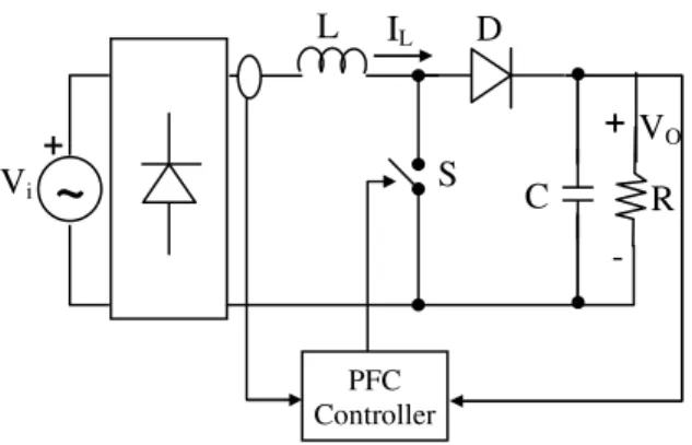
Working principle, topology in APFC: Most commonly used APFC topology namely is a single switch Boost converter. A simplified schematic of a single switch APFC is shown in Fig. 1.
Fig. 1: Active power factor corrector
Assume that by a suitable starting control strategy a DC side voltage Vo (which should be greater than the maximum of AC line i.e. Vm for proper operation of this converter) has been created. Now if the Switch ‘S’ is kept on the current in the Inductor increases from whatever it was at the instant of switch closure. Hence it is possible to increase the current in ‘L’ by closing the switch. And if the switch ‘S’ is opened, whatever current that was flowing in the Inductor at the instant of opening the switch will force itself into Capacitor ‘C’ through diode ‘D’ since current in Inductor can not be broken instantaneously in a system which is devoid of Impulse voltages. But then if ‘D’ conducts across ‘L’ changes polarity (because Vo is assumed to be more than Vm) hence current in it decreases from its initial value. Thus it is possible to increase current in ‘L’ by closing ‘S’ and to decrease the current in ‘L’ by opening the switch ‘S’. If it is possible to raise or lower the inductor current, track a pre-specified wave shape by controlling Switch on/off.
Using this strategy the current in L in this converter is made to follow a full wave rectified wave shape. If the current in L is full wave rectified in shape the line
current in the AC side will be pure sinusoidal and in phase with supply voltage due to the modulation process involved in the controlled rectifier. This is the principle of operation of Boost type single phase PFC circuit.
Boost converter design, analysis and mathematical model description: A Small signal model of Boost converter is presented here. The boost converter model quantities may be identified in Fig. 2. as:
Vi: APFC input in half sine = VmSin πt/TL D : Average duty ratio for one half line cycle Vc: Capacitor voltage equal to output voltage
i.e Vc= Vo.
IL: Average Inductor current
Fig. 2: Black box model of the converter
The boost converter is operating in continuous conduction mode (CCM).The dynamic elements in the converter are L and C. The dynamic variables in the converter are IL and Vc = Vo. So, the dynamic and output equations are written as in[8] given below:
1 i
L
c
d i D
dt L L
υ υ −
= +
1
c c
L
d D
i
dt C RC
υ = − − υ
Because of the PFC operation, there exists an unbalance of Instantaneous power between the input power, which is time varying and DC output power. Therefore PFC involves processing input power in certain way that it stores the excessive input energy when the input power is larger than DC output power and releases the stored energy when the input power is less than DC output power. To accomplish this a capacitor ‘C’ is introduced as a reservoir in APFC to take care of Dc load demand / load fluctuations..
To smoothen the variations in charge and discharge current in the capacitor, the inductor ‘L’ is introduced in APFC after bridge rectifier. That means inductor and capacitor whose role is to smooth out the inherent pulsating behaviour originating from the switching action.
APFC example design specifications * Input voltage: 85V- 135VAC * Input Power factor: >0.95
* To conform IEC 61000-3-2 Harmonic Distortion specifications
* Output voltage: 200VDC+/-2% * Peak-peak output ripple: <5%
L, C, R Vi
D
VC
1677
L
D
C * Output power: 400W
* Switching Frequency: 20Khz * Efficiency: >95%
* Isolation: Since 110V Input, it is provided through Transformer. Otherwise it is not required.
Boost converter analysis and typical characteristics wave form: For Boost converter circuit operation, the power is supplied to the converter at a DC voltage (Vi) i.e. Vi =Vm Sin (πt/ TL) where TL = AC line period and Vm = AC peak voltage. The converter feeds power to a load R at a voltage of Vo. The switch is operated at a high switching frequency with a switching period Ts. The switch is kept ON during a fraction (d.Ts) of the switching period. For the rest { (1-d) Ts } of the switching period, the switch is OFF.
The circuit operation can be divided into two modes. Mode1, Fig. 3a, begins when the Switch S is turned on at t = 0. The input current, which rises, flows through the Switch S.Mode2, Fig. 3b.begins when the transistor is switched off at t=t1 .The current which was flowing through the Switch S would now flow through L, C and load, and the diode D. The inductor current falls until the Switch S is turned on again in the next cycle. The energy stored in inductor L is transferred to the load.
Steady state (DC) analysis and volt- second balance on boost inductor: From Faraday’s law for Inductor Voltage
VL =L diL/ dt and Integration over the full period Ts, we get
1/L VL dt = diL = I L (Ts ) – IL (o) = 0 (1) Since in the steady state, the initial and final values of Inductor current must be equal. Removal of finite (non-zero) proportionality constant ‘L’ in (1) results in general criterian for the steady state, the so-called volt-second balance on the Inductor, as:
VL dt = 0 volt-second balance on the Inductor (2) or for the two switched intervals,
VL dt = - VL dt
Volt- Second stored = Volt- Second released Vi D TS = ( VO – Vi ) ( 1-D) TS
===> VO / Vi = 1/ (1-D) (3)
Fig. 3: Boost converter
Fig. 3a: Mode 1 operation
Fig. 3b: Mode 2 operation
Evaluation of switching ripple at output: If the APFC circuit operates properly and Power factor is unity, we can write power balance equation for Input and output of converter as:
VO IO = Vi IL = Vm sin (πt/ TL ) Im sin (πt/ TL ) = Vrms Irms - Vrms Irms cos ( 2 π t/ TL )Therefore Output voltage
VO = Vrms Irms - Vrms Irms cos ( 2 π t/ TL ) / IO (4) In the equation (2) the first term is DC voltage and Second term is ripple voltage. However the small switching ripple converter (typically specified to be less than 5% ) directly translates into the idealized rectangular voltage waveform and triangular current wave form on the Inductor seen in fig.4. The rising and falling slopes of the Inductor current ripple are easily deduced from the corresponding linear switched network to be Vi /L ( for D TS interval ) and ( VO – Vi )/L ( for ( 1-D) TS interval ). Ripple voltage is being neglected, as the output voltage is very higher than ripple voltage value. The selection of adequate output capacitor value in the circuit and switching frequency will help to reduce the output ripple
Since, δ VO = TS. I Omax / C. (5)
Effect of parasitic on voltage gain and efficiency: For example The DC voltage gain of the boost converter (3) becomes infinitely large when the duty ratio D approaches unity, clearly a physically incorrect result. However the inclusion some dissipative elements, such as parasitic resistance (RL) of the inductor, corrects this problem. The efficiency of course, is now reduced from original 100% because of the IL RL on the inductor resistance to:
OUT
OUT LOSS
p
p p
η=
+ =
2
2 2
/
/ /
V R
V R+I R (6)
V
iV
0L
From the inductor and diode current waveforms in Fig. 4, the ratio of the average inductor current IL and the load current I becomes
1 1
' (1 )
L
I
I = D = −D
Since the output voltage Vo and Input Voltage Vi are interrelated
with numerical constant, The efficiency becomes η = 1/ 1+ α/(1-D)(1-D)
where α nearly = RL/ R (7)
By use of this result, since efficiency is alternatively η= VO I / Vi IL, the voltage gain becomes:
1 (1 )
L i
I V
V = I η= −D 2 2
1 (1 )
(1 )
1 /(1 )
D D
D α
α
− =
− +
+ − (8)
As seen in Fig. 5 the voltage gain DC gain now correctly exhibits a maximum value over the Duty ratio D range. Also the efficiency is seen to decrease significantly for higher duty ratio.
Fig.4 Boost converter characteristics waveforms
Two level controller design: The Two level controller design is adopted here. The voltage mode controller senses APFC out put voltage, increases the Inductor current from the AC line if out put voltage tends to decrease from the set value VO(specified voltage) and decreases the current from the AC line when the output voltage tends to increase. The current mode controller
sees the Inductor current has the desired wave shape as the voltage waveform and the amplitude as commanded by voltage mode controller.
Now we shall see how the PWM (switch ON/OFF time) can be designed to achieve the controller objectives. We operate the circuit under current mode control and, to make the reference current (instantaneous value of Inductor current) equals instantaneously desired sine wave current. This approach leads to Input current to APFC that approximated to a rectified sinusoid in phase with voltage.
Now, Vi = Vmsin πt/TL
Where Vm= Amplitude of AC line, TL = frequency of AC line.
If the circuit operates properly and PF=1, there must exist a linear relationship in each switching cycle between the average value of Inductor current and Input voltage, IL = gi Vi and analogously between the low frequency components, these quantities
In (t) = gi vi(t) (1)
Fig. 5: Voltage gain and efficiency of the boost converter
Fig. 6.a: Voltage mode controller and power circuit lab. Prototype
dT
sd'T
sv
gt v
g-v
t
t
t
t
i
LI
i
Li
Li
Si
Di
Lv
Lv
gate0
0.5
1-
√α
1.0
0
1/(2
√α
)
V/Vg
0
0.5
1.0
0
η
ηη
η
low
D
1679 Here gi denotes the proportionality factor being the input conductance of the circuit (valid for low frequency components). The proportionality factor gi is varied one cycle to other i.e. every TL second (line period) so as to regulate output voltage Vo around specified value. For a steady state operation, gi must be constant independent of the considered cycle.
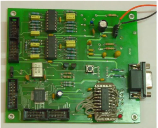
Fig. 6b: DSP hardware lab. Prototype
In inner current mode controller, we assume,
Iref (t) = I (t) (2)
For inductor continuous current mode operation,
Vi = (1-D) Vo (3)
Therefore,
(1) Becomes In(t) = gi Vo (1-D) (4) If Vi and Vo are fixed, Inductor current and the output power can be adjusted by controlling dTs (which in turn alters gi).
The average switch current can be related with Inductor current i.e.
IS = D In(t) (5)
From (4) & (5), it can be shown
IS = Vo gi (1-D) = gi Vo (1-dTs) (6) (6) gives the required relationship between IS and dTs in order to keep gi constant in a steady state operation independent of the considered cycle.
For practical implementation, from (2)
Iref (t)= gi Vo (1-dTs) = vc. vramp (7) The waveform Iref(t) is similar to ramp function of classical PWM switching mode converter, but the amplitude is adjustable and is controlled by vc(t). Thus the switch current can be compared with Iref(t) so that dTs will be determined in accordance with the above relationship.
As shown in (7), Iref(t) is derived from the product of feed back controller input vc(t) which gives the control action (gi Vo) in steady state, and a standard ramp function vramp(t) that generates a function of (1-dTs) is called PWM of the switch. Also it is known that Inductor current to follow sine wave voltage Vi in phase at start of line half cycle, Zero crossing detector (ZCD) is used to detect current reference start point. Input voltage variations and Dc load variations are considered
as disturbance input of APFC. Hence APFC controller is to regulate output voltage and track inductor current in phase with AC Mains through PWM switching for any step change in the disturbance.
CONTROLLER DESIGN IMPLEMENTATION Hardware: The complete schematic diagram of proposed a DSP based APFC is presented in Fig. 6. The voltage mode controller is implemented with IC3845 and current mode controller can be implemented through DSP. The modular construction of PCBs in this design makes easy serviceability. There are three signals as listed below, required to be sampled by DSP for current controller design.
Voltage controller output is the amplitude command required to maintain Output voltage of the APFC, received from IC3845 (pin6) as pulse width connected through opto-isolator to the capture unit of DSP (pin 4) as input. This is updated at every zero crossing point of Rectifier output. That means the voltage controller output is kept constant at that particular cycle of Rectifier output (Vi ).The voltage controller output is used of previous cycle.
Inductor Current is sensed through Hall effect sensor (HES) connected to analog conditioning unit then to ADC input of DSP (Pin No 18).
By sampling rising mono shot pulse ,zero crossing point is detected .The mono pulse is generated from Rectified output connected to zero crossing detector and mono pulse detector through a control voltage transformer.
Figure 6.a and Fig 6.b are shown laboratory prototype voltage mode controller with power circuit and DSP based hardware for current mode controller implementation respectively.
Software: The software required for current mode controller module (main module required for PFC) implementation consists of series of sub module programs performing individual tasks. These sub-modules are linked together under the control of a main program to perform as complete system. The modular program makes the software more manageable and portable.
Based on the functionality, the main current mode controller can be divided into two parts. The first part is the DSP initialization, which includes register, interrupt and subroutine Initialization. These tasks are done once the program starts.
Upon completion of initialization, the program waits for interrupt calls while performing infinite loop. The initialization routine flow diagram is shown in Fig. 6.2.
DSP TMS320
LF2403
Opto coupler /
driver
Zero crossing detector
Mono shot pulse
ADC 0
IC 3845
Opto coupler
CAP 1 CAP 3
~
Vi
L
C R
VO
D
S +
-
IL
+
~
Vi
When an interrupt occurs, the main program breaks the infinite loop and goes to the proper interrupt service routine that has been designated to the particular event. Upon finishing the routine, the program continues the infinite loop waits for the next interrupt call.
Fig. 6.2: Initialization routine flow diagram
Fig.6 Schematic diagram of the proposed DSP based APFC
Fig. 7 A DSP based Current Controller Algorithm (To be implemented on TMS 320LF2403 EVM)
Vc : Voltage controller output from IC3845.
IRef : Reference current generation synchronized with APFC input voltage Vi.
Is(t) : Current sampling. Kp : Proportional Constant. C : DSP Compare unit.
Fig.8 current controller software flow diagram
Current controller algorithm is to be implemented is shown in Fig. 7. The software interrupt routine flows are shown as in Fig. 8. It utilizes the timer interrupt routines that are called at different frequencies. Timer1 interrupt has the same frequency as the IGBT switching frequency. The capture Timer2 interrupt provides the multiplier the voltage controller output as pulse width.
CONCLUSION
A low cost digital design solution for APFC is presented for implementation for industry involved in manufacturing of SMPS/UPS. For voltage mode controller testing, input voltage given is 115VAC. Output voltage is regulated at 200V DC for load of 1.5Amp. Input voltage is varied from 80V to 135VAC and the output voltage remained at 200V and boost operation is verified. Current mode controller using DSP TMS320LF2403 can be implemented as per algorithm. The DSP is used for current mode controller design and the current mode controller is contained with in the software. By implementing PFC at low cost
Start
Infinite loop
( Waiting for Interrupt) Initialization process
- Interrupt vectors - Registers/variables
- Define Subroutine and peripherals(Timer, Capture units, ADC units)
Σ
Is(t)
Vc (CAP1)
sin ωt Table
Non-sinusoidal
IRef(t)
Kp
Σ
Limiter C PWM
25000Hz Ramp Compen
sator
Sample is
Update sine
Multiplier
Zero crossing point flag? Sine table
pointer reset
Current loop controller
PWM (IGBT) gate signal generation
comparator
Sample zero crossing
point
No update in voltage loop controller output
update in voltage loop controller
output
1681 in non-PFC based SMPS/UPS, it complies to International agency regulation and become energy efficient.
For improvement, the saved resources of DSP can be utilized to control DC/DC converter (for SMPS) and DC/AC converter (for UPS) plus front-end man-machine interface (for SMPS/UPS) and to integrate the converter with Computer as system for monitoring its status in a limited cost. Also voltage mode controller and zero crossing point detection can be implemented with DSP itself later.
Therefore APFC in a reduced hardware to minimum, increases the reliability, hence the cost by achieving high Input power factor and reduced Input current harmonics.
ACKNOWLEDGEMENT
The authors gratefully acknowledge the valuable advice, support and encouragement of Dr.R.Arumugam, School of Electrical and Electronics Engineering and Dr.D.Rajapaul Perinbam of School of Electronics and Communication Engineering of Anna University, Chennai (India).
REFERENCES
1. Mohan, N., T.M. Underland, W.P. Robbins, 1995. Power Electronics Converters, Applications and Design. 2nd Edn. New York, Wiley.
2. Suresh, Kumar, K.S. Dept. of Electrical Engg.NIT, Calicut (India). Design of active power factor corrected front end converter in UPS systems. 3. Zaszlo Balogh’s Design Note “Unitrode
UC3854A/B provide power limiting with sinusoidal input current for PFC front ends- revised Nov.2001.
4. Susilo, V.S. and P.N. Enjeti. Advanced DSP based single phase powerfactor correction approach. Dept. of Electronics Engg.Texas AM University. 5. Angel, de Castro, P. Zamel and O. Garcia, 2003.
Concurrent and simple digital controller of an AC/DC converter and PFC based on an FPGA. IEEE Trans. Power Electron., 18: 1.
6. Jinghai, Z., Z. Lu, Y. Ren and Z. Qian, 2001. Novel sampling algorithm for DSP controlled 2 KW PFC converter. IEEE Trans. Power Electronics, 16: 2.
7. Ramesh, K.T., S.P. Das and G.K. Dubey, 2002. Mixed mode operation of boost switch mode rectifier for wide range of load variations. IEEE Trans. Power Electronics, 17: 6.
8. Ramanarayanan, V. Modelling and control of Switched mode converters. Power Electronics Module-7 IMPACT.
9. J.Kassakian , M.Schlect and Verghese, “Principles of Power Electronics” Norwell,MA, addition Wesley 1991.
10. D.Y.Qiu, S.C.Yip, Hendry Chung and Syron Hui “Single current sensor control for single phase APFC” IEEE Transactions on Power Electronics Vol.-17, No.5 Sept. 2002.
11. TMS 320LF240x DSP controllers user’s manual ,Texas Instruments 2002.
12. TL284x,TL384x Current mode PWM controllers Data sheet, Texas Instruments, 1999.
13. Andres Lindemann “Rectifiers with power factor correction”, IXYS Semiconductors GMBH Doc.No.D2005E.