Novel Low Power Comparator Design
using Reversible Logic Gates
Nagamani A N#1, Jayashree H V#1,H R Bhagyalakshmi#2
#1
PES Institute of Technology,
100 ft Ring Road Bangalore,Karnataka,India
#2
BMS college of Engineering, Bull temple road, Bangalore,Karnataka,India
#1 nagamani@pes.edu #1 jayashreehv@pes.edu #2 hrbbmsce@gmail.com
Abstract— Reversible logic has received great attention in the recent years due to its ability to reduce the power dissipation which is the main requirement in low power digital design. It has wide applications in advanced computing, low power CMOS design, Optical information processing, DNA computing, bio information, quantum computation and nanotechnology. This paper presents a novel design of reversible comparator using the existing reversible gates and proposed new Reversible BJN gate. All the comparators have been modeled and verified using VHDL and ModelSim. A comparative result is presented in terms of number of gates, number of garbage outputs, number of constant inputs and Quantum cost.
Keywords— advanced computing, Reversible logic circuits, reversible logic gates and comparator.
1. INTRODUCTION
Conventional combinational logic circuits dissipate heat for every bit of information that is lost during their operation. Due to this fact the information once lost cannot be recovered in any way. But the same circuit if it is constructed using the reversible logic gates will allow the recovery of the information. In 1960s R. Landauer demonstrated that even with high technology circuits and systems constructed using irreversible hardware, results in energy dissipation due to information loss [1].He showed that the loss of one bit of information dissipates KTln2 joules of energy where K is the Boltzman’s constant and T is the absolute temperature at which the operation is performed [1]. Later Bennett, in 1973, showed that this KTln2 joules of energy dissipation in a circuit can be avoided if it is constructed using reversible logic circuits [2].
A reversible logic gate is an n-input, n-output logic device with one-to-one mapping. This helps to determine the outputs from the inputs but also the inputs can be uniquely recovered from the outputs. Extra inputs or outputs are added so that the number of inputs is made equal to the number of outputs whenever it is necessary. An important constraint present on the design of a reversible logic circuit using reversible logic gate is that fan-out is not allowed. A reversible circuit should be designed using minimum number of reversible gates. One key requirement to achieve optimization is that the designed circuit must produce minimum number of garbage outputs. Also they must use minimum number of constant inputs [3, 4].
The reversible comparator proposed in this paper is designed with an idea of retaining two of the three outputs considering any one of them redundant. This novel idea optimizes the design in terms of gate count, garbage output, constant input and quantum cost. The present paper proposes several alternate designs of a comparator circuit using existing reversible logic gates.The Present paper proposes a new gate, called Reversible BJN gate which is used in the design of comparator along with the existing Reversible gates. This work proposes various comparator designs and compared for their performance parameters. All the proposed designs are virtually implemented using VHDL and functionally verified using ModelSim simulator.
This paper is organized as follows:
2 BASIC REVERSIBLE LOGIC GATES
2.1 Reversible logic gate
It is an n-input n-output logic function in which there is a one-to-one correspondence between the inputs and the outputs. Because of this bijective mapping the input vector can be uniquely determined from the output vector. This prevents the loss of information which is the root cause of power dissipation in irreversible logic circuits. In the design of reversible logic circuits the following points must be considered to achieve an optimized circuit. They are
Fan-out is not permitted.
Loops or feedbacks are not permitted
Garbage outputs must be minimum
Minimum delay
Minimum quantum cost.
2.2 Basic reversible logic gates
Some of the important basic reversible logic gates are, Feynman gate [5 ,6], Fredkin gate [4] and Toffoli gate [3], Peres gate [6] , R- gate[ 7], URG [8] gate and TR gate [9].
2.2.1. Feynman / CNOT Gate:
Fig 2a shows the Feynman gate which is a 2*2 gate and is also called as Controlled NOT and it is widely used for fan-out purposes. The inputs (A, B) and outputs P=A, Q= AB. It has Quantum cost one.
Fig. 2a1. Feynman Gate – 2*2 gate Fig 2a2. Quantum implementation of Feynman Gate
2.2.2. Peres Gate: Fig 2b shows a Peres gate which is a 3*3 gate having inputs (A, B, C) and outputs P = A ,
Q = AB, R = ABC. It has Quantum cost four.
Fig. 2b1. Peres Gate – 3*3 gate
Fig:2b2. Quantum implementation of Peres Gate
2.2.3. Toffoli Gate: Fig 2c showsa Toffoli gate which is a 3*3 gate with inputs (A, B, C) and outputs P=A,
Q=B, R=ABC. It has Quantum cost five.
Fig. 2c1. Toffoli Gate – 3*3 gate
Q=A'B+AC, R=AB+A'C. It has Quantum cost five.
Fig. 2d. Fredkin Gate – 3*3 gate
Fig.2d2. Quantum implementation of Fredkin Gate
2.2.5. R Gate: Fig 2e shows an R-gate which is a 3*3gate with inputs (A,B,C) and outputs P= AB, Q= A, R
= C’AB. Quantum cost of this gate is not mentioned by the author.[7]
Fig. 2e1. R Gate – 3*3 gate
*Note: Quantum implementation of R gate is not discussed by author[7]
2.2.6. URG Gate: Fig 2f shows an URG gate which is a 3*3 gate with inputs (A, B, C) and outputs P= (A+B)
C, Q= B, R = AB C. Quantum cost of this gate is not mentioned by the author.[7]
Fig. 2f1. URG gate – 3*3 gate
*Note: Quantum implementation of URG gate is not discussed by author[7]
2.2.6. TR Gate:
The fig 2g shows a 3*3 gate with inputs (A, B, C) and outputs P=A, Q=AB, R= AB'C. It has Quantum cost six.
Fig. 2g1. TR Gate - 3*3 gate
Fig.2g2. Quantum implementation of TR Gate
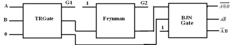
2.2.7 New BJN Gate:
Fig. 2e1. BJN Gate - 3*3 gate
Figure 2e2. Quantum realization of BJN gate
Table 1 . Truth table of BJN gate
A B C P Q R
0 0 0 0 0 0 0 0 1 0 0 1 0 1 0 0 1 1 0 1 1 0 1 0 1 0 0 1 0 1 1 0 1 1 0 0 1 1 0 1 1 1 1 1 1 1 1 0
3.DESIGN OF ONE - BIT COMPARATOR
3.1 Implementation of One-bit Irreversible Comparator
The conventional one-bit irreversible numerical comparator, which consists of two NOT gates, two AND gates and one NOR gate [10], is shown in Fig.3a with its truth table in Table 2. We can get the following logic expressions from Table 2.
--- --- (Eq1)
Table 2. Truth table of 1- bit comparator
It is observed from the above table that, if any two conditions are not satisfied, it is understood that the third condition will be true. So one of the outputs can be generated from the remaining two outputs and thus the design can be optimized.
In the proposed one-bit comparator design, we have considered FA>B and FA=B and the third condition FA<B is
This design requires one NOT gate, one AND gate and one ENOR ( Ex-Nor) gate and one NOR gate.
Fig.3.1 a. Irreversible gates for Numerical comparator
3.2 The proposed one bit Reversible comparator designs
All the gates mentioned in section 2 can be used for the construction of reversible comparators. Here the proposed BJN gate is used in the last stage of comparator to generate all the outputs of comparator. Using this gate in combination with existing reversible gates, garbage output, quantum cost and gate counts are reduced.
3.2.1. One- bit comparator using Peres and BJN gate
Reversible one bit comparator is implemented with Feynman gate and Peres gate and BJN gate as shown in fig.3.2a. The number of garbage outputs are two and represented as G1 and G2, it uses three constant inputs one logic ‘0’ and two logic ‘1’.
Fig. 3.2a. one bit comparator using Peres gate
3.2.2. One bit comparator using Toffoli and BJN gate
Reversible one bit comparator is implemented with Feynman gate and Toffoli gate as shown in fig.3.2b. The number of garbage outputs are two and represented as G1 and G2, it uses three constant inputs , one logic ‘0’ and two logic ‘1’ it requires one Feynman gate and two Toffoli gates.
Fig. 3.2b.one bit comparator using Toffoli gate
3.2.3.one bit comparator using R and BJN gate
Reversible one bit comparator is implemented with Feynman gate and R gate as shown in fig.3.2c. The number of garbage outputs is two and represented as G1, it uses two constant logic ‘1’ input. It requires one Feynman gate and one R gate.
3.2.4.One bit comparator using URG and BJN gate
Reversible one bit comparator is implemented with Feynman gate and URG gate as shown in fig.3.2d. The number of garbage outputs are three and represented as G1,G2 and G3.It uses Four constant inputs two logic ‘0’ and two logic ‘1’. It requires one Feynman gate and two URG gates and one BJN gate.
Fig. 3.2d. one bit comparator using URG gate
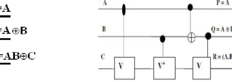
3.2.5. One bit comparator using Fredkin and BJN gate
Reversible one bit comparator is implemented with Feynman gate and Fredkin gate and BJN gate is as shown in fig.3.2e. The number of garbage outputs are six and represented with G1 to G6, it uses seven constant inputs, four logic ‘0’ and three logic ‘1’. Two Feynman gates are used for fan-out purpose in the input part.
Fig.3.2e. one bit comparator using Fredkin gate
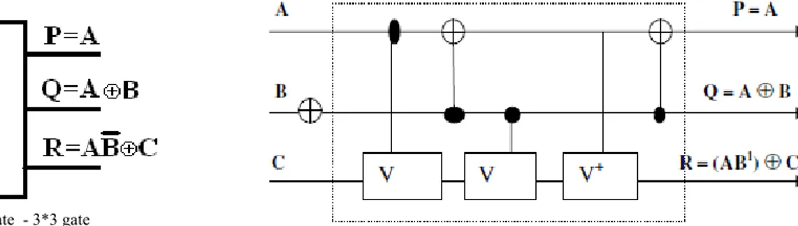
3.2.6. one bit comparator using TR and BJN gate
Reversible one bit comparator is implemented with Feynman gate and TR gate and BJN gate as shown in fig.3.2f. The number of garbage outputs are two and represented with G1 and G2, it uses three constant inputs, one logic ‘0’ and two logic ‘1’.
Fig. 3.2f. one bit comparator using TR gate
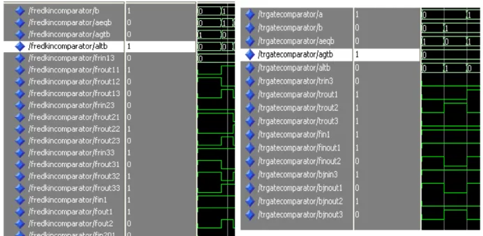
4. SIMULATION RESULTS
Reversible one bit comparators proposed and Reversible 4-bit equality comparator proposed in section 3 are implemented using VHDL and Simulated using Modelsim Simulator. The individual gate functionality and the overall logic is implemented using Structural style of Modeling and simulation results are shown in fig.4.1 to 4.6.
4.1 one- bit comparator using Peres and BJN gate 4.2 one bit comparator using Toffoli and BJN gate
Fig.4.1. Simulation result of 1- bit comparator using Peres and BJN gate
4.3 one bit comparator using R and BJN gate
4.4 one bit comparator using URG and BJN gate
Fig 4.3. Simulation result of one bit comparator using R and BJN gate
Fig. 4.4. Simulation result of one bit comparator using URG and BJN gate
4.5 one bit comparator using Fredkin and BJN
Gate 4.6 one bit comparator using TR and BJN Gate
Fig.4.5 Simulation result of one bit comparator using Fredkin and BJN Gate
Fig. 4.6. Simulation result of one bit comparator using TR and BJN gate
5. RESULTS COMPARISON AND DISCUSSION
Garbage Outputs: This refers to the number of outputs which are not used in the synthesis of a given function.
These are very essential without which reversibility cannot be achieved. Gate count: The number of reversible gates used to realize the function.
From the comparison results of all comparator designs shown in table3 and chart 1 , it is compared in terms of gate count, Garbage output and number of constant inputs. It is evident from the results from Peres with BJN is optimized design in comparison with other designs.
Table 3. Comparison Results
*Quantum cost of R and URG gates are not specified by the authors .[7]
Chart 1. Comparison Results
6. CONCLUSION
In this paper an optimized reversible comparator is presented with the proposed new Reversible BJN gate. The design is very useful for the future computing techniques like ultra low power digital circuits and quantum computers.
It is shown that the proposal is highly optimized in terms of number of reversible logic gates, number of garbage outputs and number of constant inputs.
The analysis of various implementations discussed are tabulated in Table-3.It gives the comparisons of the different designs in terms of the important design parameters like number of reversible gates, number of garbage outputs and number of constant inputs and quantum cost. The performance parameters are optimized in comparison with the existing numerical comparator [10 ].
.
REFERENCES
[1] R. Landauer, “Irreversibility and Heat Generation in the Computational Process”, IBM Journal of Research and Development, 5, pp. 183- 191, 1961.
[2] C.H. Bennett, “Logical Reversibility of Computation”, IBM J.Research and Development, pp. 525-532, November 1973. [3] T. Toffoli., “Reversible Computing”, Tech memo MIT/LCS/TM-151, MIT Lab for Computer Science 1980.
[4] E. Fredkin and T. Toffoli, “Conservative logic,” Int’l J. Theoretical Physics, Vol. 21, pp.219–253, 1982. [5] R. Feynman, “Quantum Mechanical Computers,” Optics News, Vol.11, pp. 11–20, 1985.
[6] Peres, “Reversible Logic and Quantum Computers”, Physical review A, 32:3266- 3276, 1985.
[7] D.P.Vasudevan, P.K.Lala, J.Di and J.P.Parkerson, “ Reversible-logic design with online testability”, IEEETrans. on
Instrumentation and Measurement, vol.55., no.2, pp.406- 414, April 2006.
[8] P. Kemtopf, "Synthesis of multipurpose reversible logic gates," Euromicro Symposium on Digital System Design (DSD'02), pp. 259-267, 2002.
one bit comparator design using existing gates with new BJN
gate Reversible gates Garbage outputs Constant inputs Quantum cost
Peres and BJN Gate 3 2 3 10
Toffoli and BJN Gate 4 2 3 16
R and BJN Gate 3 1 2 *
URG and BJN Gate 4 3 4 *
Fredkin and BJN Gate 5 6 7 23
[10] Lihui Ni, Zhijin Guan, XiaoyuDai, Wen juan Li, “Using New Designed NLG Gate for the Realization of Four-bit Reversible
Numerical Comparator” Wen juan Li”,2010 International Conference on Educational and Network Technology (ICENT 2010).