SPECTRAL ANALYSIS OF BUCK AND
SEPIC CONVERTERS
CHAKIB ALAOUI
College of Computers and Information Technology Taif University, KSA
chakib@tu.edu.sa Abstract:
Switched mode power converters generate harmonic currents, which will be injected into the utility grid, causing distortion of the utility waveform. They also become a source for the generation of EMI, which may affect the communication systems. This work is about the design and evaluation of the two most frequently used SMPS used in step down mode of operation: the Buck converter and the Sepic converter working in step-down mode of operation. These converters were designed using optimized equations for their components ratings. Simulation results show that although the Buck output voltage is low in harmonics, it has high harmonic contents in currents circulating in its inductor and diode, and hence requires strong filtering. The Sepic converter has lower harmonic contents than the Buck converter.
Keywords: Switched Mode Power Supply; Buck Converter; Sepic Converter; Harmonics.
1. Introduction
Many electronic applications require switched-mode power supplies (SMPS). The SMPS have some interesting advantages like: power efficiency, small size, light weight and low heat generation. They have also some disadvantages like: complexity, ripple voltage at switching and harmonic frequencies, electromagnetic interference with audio and video equipments [Sugasawara et al (1996)] and [Khan-ngern W. (2002)].
They are widely used especially for their efficiency. For these noisy equipments, electromagnetic interference (EMI) filters were designed to comply with the international electromagnetic compatibility (ECM) standards. [Nasiri, (2005)] The purpose of this work is to make a harmonics assessment of two common DC-to-DC converters: Buck and Sepic converter working in step-down mode of operation. An overview of the design equations of these converters was given. These equations satisfy optimal operating points of the converters. Then these converters were designed to satisfy a same application, in other words having similar Vin, Vout, Iout and with the same switching frequency. Finally the two converters were investigated in terms of their power spectrum.
2. Buck converter design
The Buck is a step-down switching converter that transfers small packets of energy using a switch, a diode, an inductor and two capacitors. Figure 1 a) shows the basic structure of a Buck converter circuit. Figure 1 b) shows the Buck converter when the power MOSFET is on for the time duration DT, where 0 D 1 and T is the period of the signal. The inductor voltage VL = VIN – VOUT. This voltage causes a linear increase in the inductor current iL. Figure 1 c) shows the converter when the switch is turned off during (1-D)T, iL continues to flow because of the inductive energy storage. This current flows through the diode, and VL = -VOUT for a time duration until the switch is turned on again. The following summarize the optimized equations used to design the Buck converter [Schelle D. et al (2006)] and [Mohan N. et al (1989)].
Fig.1 Buck converter.
2.1 Inductor
Calculating the inductor value is most critical in designing a Buck converter. Assuming that the converter is in continuous conduction mode, or CCM in short, the inductor does not fully discharge during the switch-off time. The following equations assume an ideal switch (zero on-resistance, infinite off-resistance and zero switching time) and an ideal diode. Eq. (1) expresses the inductor value.
Where fsw is the switching frequency, LIR is the inductor-to-current ration expressed as a percentage of Iout.
Peak current through the inductor determines the inductor's required saturation-current rating and the size of the inductor. Saturating the inductor core decreases the converter efficiency, while increasing the temperatures of the inductor, the MOSFET and the diode. The peak and the ripple currents in the inductor are expressed in Eq. (2)
2.2 Output Capacitor
Output capacitance is required to minimize the voltage overshoot and ripple present at the output of the Buck converter. Large overshoots are caused by insufficient output capacitance, and large voltage ripple is caused by insufficient capacitance as well as a high equivalent-series resistance (ESR) in the output capacitor.
The problem of overshoot, in which the output-voltage overshoots its regulated value when a full load is suddenly removed from the output, requires that the output capacitor be large enough to prevent stored inductor energy from launching the output above the specified maximum output voltage. Output-voltage overshoot can be calculated using the following Eq. (3).
!"#$%&'() *)
+,-. )
It follows the value of the output capacitor expressed in Eq. (4).
/ 01 ) & ) *)*
(1)
(2)
(3)
2.3 Input capacitor
The input capacitor’s ripple-current rating dictates its value and physical size, and Eq. (5) calculates the amount of ripple current the input capacitor must be able to handle
+ 2 3 4
3. Sepic converter design
Figure 2 shows the basic SEPIC topology. Figure 2 b) shows the steady-state during the switch (SW) on-time (DT), energy is stored in inductor L1. The inductor currents iL1 and iL2 ramp up at a slope determined by the input voltage and the inductances L1 and L2. The L2 inductor current ramps up at the same rate through coupling capacitor Cc and SW. The Cc positive terminal is at ground potential, and the voltage across L2 is VIN, which is the same as the voltage across L1. At this point in time, the output capacitors supply the load current while diode D is reverse biased. Figure 2 c) shows that when the SW turns off ((1-D)T), diode D is forward biased, and it conducts the energy stored in both inductors to the load while also charging the output capacitor. The voltages across the inductors are clamped to output voltage with the same inductor down-slope currents. The following summarize the equations used to design the Buck converter. [Moussa W.M. (1995)] and [Chung H.S. et al (2003)].
Fig. 2. Sepic Converter
3.1 Duty cycle
In a CCM SEPIC converter, the maximum duty cycle will determine the component current ratings and impact the maximum voltage stress on the switching elements. Eq. (6) shows the duty cycle as function of the voltages.
5 6
6
Where D is the duty cycle, VOUT the output voltage, VD the forward voltage of the diode and VIN the input voltage of the converter. The maximum output voltage is expressed in Eq. (7).
6 7866"#$"#$ 6 7867"#$
(6)
3.2 Inductors
The maximum currents in inductors L1 and L2 are calculated in Eq. (8).
7 9: ; <1 +=> ∗ ( )∗?? !%?@ AB(CDE)
(9: ;)= <1 +F2> ∗ ( )∗ ( HI)+ 6 (JKL)
Where 20% 40%. The inductor current is calculated according to Eq. (9) and (10).
=?AB("MN) ∆(∗P ∗ 5 Where:
∆ = )F ∗ Q( )∗1 − 55
Usually, L1 = L2 and their winding is on the same core. The mutual inductance is 2L, and the inductance is expressed in Eq. (11)
1 = 2 =2 ∗ ∆ ∗ ∗ 5( HI)
The power MOSFET must satisfy Eq. (12).
6 (QI)≤ 3:I3:( ) ( ) ∗
1 (1 + F2)S ∗
1 + 6 ( HI) + 1
Where Vsense(max) is typically 150mV at low duty cycle and 100mV at maximum duty cycle. T is the temperature coefficient 0.4%/°C. In order to obtain a maximum duty cycle, a fast switching diode with low forward voltage and low reverse leakage current is used in this type of converter. The peak reverse voltage is Vin(max) + Vo. The average forward current is expressed in Eq. (13).
6(9: ;)= <1 +F2> ∗ ( )∗ ( + 6 ( HI) + 1)
3.3 Output capacitor
The parameters of the capacitor have a contribution on the ripple voltage of the converter. These parameters are: bulk capacitance, ESR (Equivalent Series Resistance), and ESL (Equivalent Series Inductance). For a 1% contribution to the total ripple voltage, the ESR of the output capacitor can be determined using Eq. (14) and (15).
TU +Q01≤0.01 ∗ 6(9: ;)
/Q01≥Y.Y7∗? !("#$) !∗PZ[
The RSM ripple current in the capacitor is given by Eq. (16).
\] (+Q01)= ( )∗ ?AB("MN)? !
3.4 Coupling capacitor
The ripple voltage in the coupling capacitor is expressed in Eq. (17).
O +^ 99 /
^∗ 3_ ∗ + + 6
The maximum voltage at the coupling capacitor is expressed in Eq. (18)
+^( )= +O +^ 99G 4. Simulations
4.1 Buck converter design and simulation
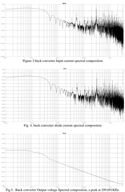
An optimized buck converter was designed by using Eq. (1 -5). The following values were obtained for Vin= 12VDC and VOUT = 5V: C1=10µ F, L=16µ F, C2=500µ F, fSW=300KHz and Rl=2.5 . The MOSFET used was IRF15003s with Rds(on)=3.3m and Ggate=0.28nC. In order to obtain 5VDC at the output, a duty cycle of D = 0.416 was used. The following figure shows the MOSFET drain current spectral composition. Figures 3, 4 and 5 show the spectral composition of the current in the MOSFET, the diode current and the output voltage respectively.
Figure 3 buck converter Input current spectral composition
Fig. 4. buck converter diode current spectral composition
Fig.5. Buck converter Output voltage Spectral composition, a peak at 299.691KHz.
(17)
4.2 Sepic converter design and simulation
A step-down Sepic converter was designed according to the optimized Eq. (6 – 18) with VIN=12VDC and VOUT=5V: L1=L2=4µ F, CIN=10µ F, COUT=300µ F, Cc=10µF, a switching frequency of 300KHz and Rl=2.5 . The MOSFET used was IRF15003s with Rds(on)=3.3m and Ggate=0.28nC.
Fig.6. Sepic converter Output voltage Spectral composition
Fig.7. Sepic converter inductor current Spectral composition
Fig.8. Sepic converter diode current Spectral composition
The spectral composition of the Sepic converter shows that the most important harmonics are located at 300.18 KHz, 599.383 KHz, 900.253 KHz, 1.197 MHz. The frequencies are observed to be n*fSW, with 1 n and fSW=300KHz in this case.
5. Discussion and conclusion
This paper has presented a design procedure for two frequently used SMPS converters: Buck and Sepic converters. Then the spectral composition of the different signals flowing in the converters is simulated with the FFT of Spice. The buck converter showed very low harmonic composition in the output voltage. However, the switching current in the inductor has very high harmonic contents, and was observed to be in the form of
in all the different parts of the circuit and were observed to be in the form of n*fSW, fSW being the switching frequency. However, their noise level is much lower than the Buck converter.
This work has shown that the Sepic converter has a reduced EMI and does not require input filters in many applications, unless the harmonic contents requirements are very severe. Meanwhile, Buck converter always requires input filters. This extra-cost makes the Sepic converter less costly than the Buck converter.
References
[1] Sugasawara D., Paetau J., (1996): Safety, EMI and RFI Considerations, Application Note 42007, Fairchild Semiconductor.
[2] Khan-ngern W., (2002): “Electromagnetic Compatibility Experimental Laboratory on Power Electronics” Proceeding of 2002 International Conference on Electromagnetic Compatibility, Bangkok, Thailand, pp. 406-411.
[3] Nasiri, (2005): Different Topologies of Active EMI/Ripple Filters for Automotive DC/DC Converters, Vehicle Power and Propulsion, IEEE Conference, pp. 168-173.
[4] Schelle D.; Castorena J. (2006): Buck-converter Design Demystified. Power Electronics Technology. pp. 46-53 [5] Mohan N., Undeland T.M. Robbins W. (1989): Power Electronics, J. Wiley Verlag.
[6] Moussa W.M. (1995): Modeling and Performance Evaluation of a DC/DC SEPIC Converter, Appl. Power Electronics Conf. and Expo. 1995, APEC ’95, Conf. Proc. 2, pp. 702 – 706.
[7] Chung H.S., Tse K., Hui S. Y., Mok C.M., and Ho M.T., (2003): “A novel maximum power point tracking technique for solar panels using a SEPIC or cuk converter,” IEEE Trans. Power Electronics, 18, No. 3, pp. 717-724.
Biographical notes
Chakib Alaoui is Assistant Professor at the faculty of computers and Information Technology at Taif University, KSA. He obtained a PhD degree from the University of Massachusetts, Lowell in 2001. His interests are in the area of analog, digital and power electronics, wind and photovoltaic energy conversion and electric vehicle technology.