SVETLANA R. LUKIĆ MILOŠ B. ŽIVANOV1 1
Faculty of Technical Sciences, University of Novi Sad, Novi Sad 2
Faculty of Sciences, University of Novi Sad, Novi Sad
SCIENTIFIC PAPER
UDC 621.382:539.213:546.56 DOI: 10.2298/HEMIND0903183S
EFFECTS IN THE CHALCOGENIDE GLASSY
SEMICONDUCTOR Cu
1(AsSe
1.4I
0.2)
99*
The current–voltage characteristics of the bulk metal chalcogenide glassy semicon-ductor Cu1(AsSe1.4I0.2)99 are obtained by Tektronix 576 Curve Tracer. It was found
that this glass has current-controlled negative resistance (CCNR) and switching cha-racteristic with memory. Experimental results have shown a strong decrease in elec-trical resistivity and threshold voltage due to the presence of the metallic element cop-per and change of ambient temcop-perature. Also, photomicrographs of the sample surface are presented and the impact of electrical switching on forming crystalline conductive channels on the surface of the investigated amorphous semiconductor is discussed.
In the group of non-crystalline semiconducting materials a special place is occupied by chalcogenide amorphous semiconductors, i.e. the materials that con-tain one or more chalcogen elements: sulphur, selenium and tellurium [1]. They can be obtained in the form of glasses either as bulk amorphous samples, or in the form of thin films.
The possibility of obtaining a large number of amorphous semiconductors of different composition, in-cluding also non-stoichiometric compounds and mixtu-res, has opened a wide perspective for the application of these materials. Scientists have discovered a lot of new chalcogenide materials, phenomena and applications. Following the development of the glassy chalcogenide field, new optoelectronic materials based on halides have been discovered. Complex oxide and non-oxide glasses have been prepared and investigated in the last several decades, thus widening the groups of materials used in various optical, electronic and optoelectronic se-miconductor glasses. The great advantages of the disor-dered materials are: simple preparation procedures, low sensitivity to impurities, high stability to the action of ionizing radiation, chemical stability towards the majo-rity of aggressive chemical substances, low cost, and the possibility to produce large area films of various thick-ness in classical systems for deposition: systems for evaporation in vacuum, magnetron systems, flash, spin-coating systems, sol–gel systems, etc. [2].
Chalcogenide glassy semiconductors have a num-ber of properties important for device application. They show continuous change of physical properties with change in chemical composition. A lot of work has been done on impurity effect on conductivity and optical pro-perties [3,4]. Electrical conductivity and switching of amorphous semiconductors depends on synthesis, melt cooling rate, purity of the starting components, thermal treatment and other factors [5–7].
*Paper presented at the “Sedmi seminar mladih istračivača” (7th Seminar of Young Researchers), Belgrade, December 22–24, 2008.
Correspondence: M.P. Slankamenac, Fakultet tehničkih nauka, De-partman za energetiku elektroniku i telekomunikacije, Trg Dositeja Obradovića 6, 21000 Novi Sad.
E-mail: [email protected] Paper received: 22 Decembеr 2008 Paper accepted: 23 January 2009
Electrical switching in chalcogenide glasses has been discovered by Ovshinsky about four decades ago [8]. Though the promised applications in information storage or power control have not been fully realized, electrical switching has remained to be one of the fasci-nating properties of these materials.
The relation between switching parameters and other properties of chalcogenide glasses has been a topic of intense investigations for long time. Several investi-gations have been directed towards understanding the relation between the switching voltages and glass tran-sition temperature [9,10], crystallization temperature [11], electrical resistivity [12], ambient temperature and conductivity activation energy [13], etc., of glassy chal-cogenides. Recently, considerable attention has been gi-ven to the understanding of the influence of two net-work topological thresholds, namely the rigidity perco-lation threshold (RPT) and chemical threshold (CT) res-pectively, on the switching behavior of chalcogenide glasses [14].
SWITCHING EFFECT
Interesting electrical switching effects have been observed in a large variety of amorphous semiconduc-tors when they had been placed as a thin layer between two electrodes [15]. Most of these switching effects have in common the fact that they are current-controlled so that the I–V characteristic is obtained with a protec-tive load resistor RL placed in series with the switching unit.
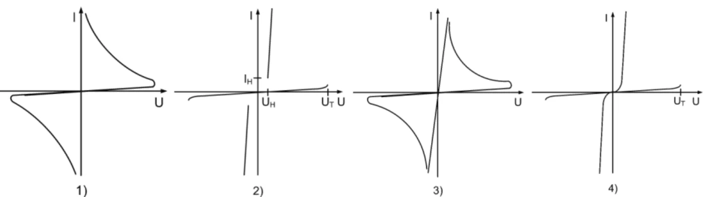
The appearance of the observed I–V characteristics suggests the fourfold classification shown in Fig. 1. The negative resistance device has an I–V characteristic which is retraceable and shows an extended negative differren-tial resistance region, see Fig. 1.1. With a proper choice of RL this negative resistance device can be kept at any point of the I–V curve. Some hysteresis is observed when the current is changed too rapidly for maintaining thermal equilibrium. With a small value of RL this device can be made to switch along the load line from a point at which –(dV/dI) = RL to the point of intersection of the load line and the I–V characteristic.
con-ductive state to which the device switches at the thres-hold voltage UT, see Fig. 1.2. The conductive state can be maintained only above a holding current IH. When I is decreased below IH, the device switches to its original high resistance state. The negative resistance device with memory has two states: high resistance and con-ductive, see Fig. 1.3.
Conductive states are established at higher currents and then remain without noticeable decay. The high-re-sistance state can be re-established by increasing the current above a certain value and switching it off rapid-ly. The switching device with memory also has two stable states, see Fig. 1.4. The initial high-resistance state and the mode of switching resemble those of the second device. The second state is conducting and per-sists without change. The high resistance state can be re--established by applying a short current pulse.
Almost all of these phenomena occur in the same manner for both polarities of the applied voltage. This phenomenological classification is, however, insufficient to separate the physical causes that give rise to the switch-ing effects.
Although self-heating of a semiconducting material whose resistivity drops rapidly with increasing tempera-ture can easily lead to thermal run-away, this need not be the only mechanism which yields to negative differ-rential resistance.
On the other hand, regardless of the physical me-chanism and despite the obvious differences among the cases shown in Fig. 1, all of these have in common the transition from the high-resistive to the conductive state that occurs with a constriction or narrowing of the cur-rent path.
The memory action, i.e. the persistence of two sta-tes in which resistances differ by many orders of magni-tude, is possible in the switching devices with memory (Fig. 1.4) only when a structural change can take place in the material. Simple binary or ternary glasses near eutectic or compound compositions are examples of suit-able materials. Simpler structures like those of elemen-tal semiconductors or stoichiometric compound mate-rials were found impractical because of their excessive
tendency to crystallize. In contrast to this, any structure change has to be inhibited in order to obtain the switch-ing effect without memory (Fig. 1.2).Examples of these materials are multicomponent glasses of alloys of Group III, IV, V and VI elements. These can be cooled very slowly from the liquid without showing traces of crys-tallite growth. The switching devices without and with memory have in common that switching occurs very abruptly at a threshold voltage, UT, when the applied voltage is increased slowly. When a square-wave volta-ge is applied, switching occurs after a delay time which decreases nearly exponentially with increasing square- -wave voltage amplitude. No switching appears possible below a certain voltage which for practical purposes is equal to UT. The switching time measured in several laboratories is less than 10-9 s [2]. This upper limit is de-termined by the response time of the measuring equip-ment. The conduction in the high-resistance state was found to be bulk limited rather than contact limited. All conductors tested were found to form low-resistance contacts with these amorphous semiconductors when precautions were taken to free the electrodes from oxide layers. Evidence for this was obtained by four-probe measurements and by testing the scaling of the resistan-ce with the film thickness.
Before switching occurs, the conductance increases approximately exponentially with applied voltage. Pulse measurements show that the temperature of the semi-conductor rises less than about 15 °C above ambient, due to self-heating before switching under static con-ditions.
The dimensions of the unit, the specific heat per unit volume of the amorphous layer, and the tempera-ture dependence of its resistivity allow us to estimate whether self-heating is a possible mechanism for switch-ing. We note that the apparently discontinuous change of slope from a positive differential resistance at the point of breakdown to a slope equal to that of the load line, already speaks against a thermal run-away.
EXPERIMENTAL AND RESULTS
The studied alloy was synthesized by the usual melt-quench method, using high-purity elementary com-ponents [1]. The non-crystalline nature of the ingot thus obtained was confirmed by X-ray diffraction and by dif-ferential scanning calorimetry (DSC) [6].
Samples used for electrical switching measure-ments were prepared in sandwich structure of electrodes [15]. The polished plate sample with thickness of 2.4 mm has contacts of Ag paste (ohmic contacts). This pro-cedure ensures correct electrical contacts, as well as easy detection of any process which could take place on the material surface, such as the growth of a low-resistance channel between the electrodes [16]. Fig. 2 shows ap-pearance of the final sample with silver electrodes.
Fig. 2. Sample’s appearance.
For DC current–voltage characteristics measure-ments a Tektronix 576 Curve Tracer is used. It is a rugged high power measurement system for tests on 2- and 3-terminal discrete semiconductors. Display area readout of test results and setup parameters decreases the chances of operator error. Voltage step ranges are up to 1500 V and current step ranges are up to 20 A peak pulse. Switchable polarity and display magnification use for more accurate resolution. Due to better results of measurement and later analysis the Curve Traces with the Sony HC-23 video camera are used.
Measurements above room temperature were un-dertaken by placing the sample holder in a thermally controlled furnace. The ambient temperature was regu-lated with a temperature controller BECKMAN CTC 250 (PID type). The temperature was measured using a copper-constantan thermocouple with accuracy of 0.5 K. All measurements were done in air and in dark.
Manual probe system PM5 - SUSS MicroTec Test Systems is used for failure analysis (FA) of the sample surface during electrical stimulation.
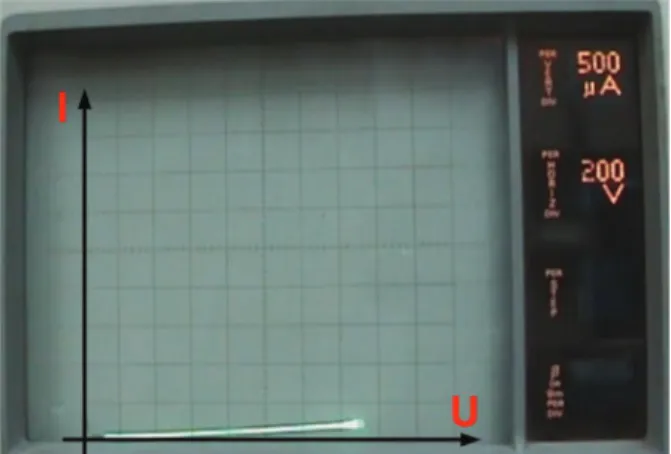
Figures 3–5 shows I–V characteristics of the sam-ple during electrical stimulation on temperature of 150 °C. This temperature is chosen because the sample has high electrical resistance and threshold voltage (over the range of the Tracer) on lower temperatures. During measurements on the cathode Tracer, the video camera records characteristics appearance from the monitor. Analysis of captured pictures (30 frames per second) is
performed by Adobe Premiere Pro 1.5 software. Maxi-mal voltage and power supply was Vmax = 1500 V and
Pmax=10 W, whereas the serial resistance was Rs = 65 kΩ. Fig. 3 depicts high resistance – “OFF” state, i.e. voltage on the sample is relatively high whereas current is low.
Fig. 3. High resistance state – “OFF”.
Fig. 4. Transient switching state.
Fig. 5. Low resistance state – “ON”.
There is a negative resistance region (voltage drop, during current rises) between the OFF and ON state, the slope of which depends on the value of the serial resis-tance. Threshold voltage is 1500 V, whereas threshold current is 250 μA approximately.
Experimental results [17] have shown a strong de-crease in electrical resistivity (which ranges from 1011 to 1012Ω cm in AsSeI glassy alloys and its value for this alloy is 1010Ω cm at room temperature), and in the se-miconductor electron mobility gap (which ranges from 0.72 eV for AsSeI glassy semiconductors and is 0.67 eV for this alloy), due to the presence of the metallic ele-ment copper. Because of these facts, it is expected of the threshold voltage to decrease as well, with increasing Cu content [18]. Threshold voltage decreases whereas current increases with the increase of ambient tempera-ture [19].
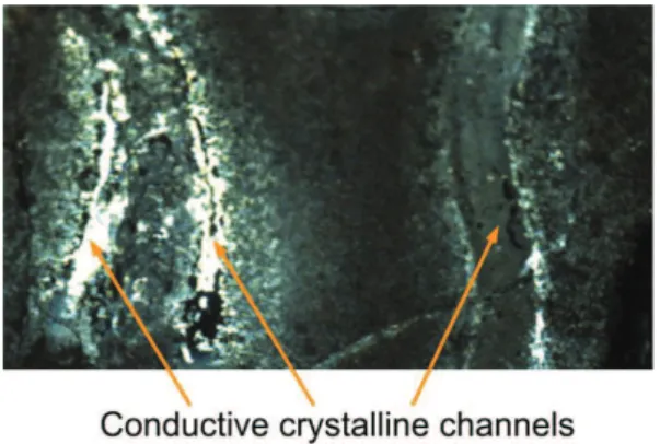
Fig. 6 shows the micrograph of the amorphous surface of the sample. Fig. 7 shows conductive channels
that appeared on the surface of the sample, after the switch-ing process had occurred in a CCNDR experiment, car-ried out with a contact electrode arrangement. The oc-currence of these channels is additional evidence of cur-rent (and so, thermal) filamentation in the material, when the CCNDR effect appears. Several regions can be observed in these micrographs: first, the amorphous matrix, i.e. the zone of the material unchanged during electrical stimulation; secondly, between both electro-des, there is a region which melted during the electrical stimulation, and re-amorphized after this stimulation was suppressed; finally, inside this melt-quenched zone, a narrow channel can be seen, showing dendrite-like growth, characteristic of crystalline materials.
CONCLUSION
Switching effects in the bulk metal chalcogenide glassy semiconductor Cu1(AsSe1.4I0.2)99 are confirmed during the electrical stimulation experiments. It was found that this glass has current-controlled negative re-sistance (CCNR) switching characteristic with memory. Experimental results have shown a strong decrease in
electrical resistivity and threshold voltage, due to the presence of the metallic element copper and the increase of ambient temperature. Also, photomicrographs of the sample surface confirm that electrical switching causes crystalline conductive channels on the surface of the in-vestigated amorphous semiconductor to appear. The next step in these investigations will be detailed exami-nation of temperature impacts on switching parameters in various amorphous samples.
Acknowledgements
This work has been carried out with the financial support of the Ministry of Science and Technological Development of the Republic of Serbia (project “Amor-phous and Nanostructural Chalcogenides”) and the Pro-vincial Secretariat of Science and Technological Deve-lopment, Autonomous Province of Vojvodina (project ”Te-chnology of obtaining and characterization of disorde-red semiconductors”), to which authors are very grateful.
REFERENCES
[1] S. Lukić, D. Petrović, Complex noncrystaline chalcoge-nides, University of Novi Sad, Faculty of Sciences, Novi Sad, 2002, p. 8.
[2] M. Popescu, J. Optoelectron. Adv. Mater. 7 (2005) 2189– –2210.
[3] B. Stričić, M. Živanov, M. Slankamenac, 8th Interna-tional Symposium Young People and Multidisciplinary Research, Timisoara, Romania, 2 (2006) 257–266.
[4] M. Slankamenac, M. Živanov, Research people and
ac-tual tasks on multidisciplinary sciences, Loznec, Bul-garia, 2 (2007) 304–309.
[5] T. Ivetić, M.V. Nikolić, M. Slankamenac, M. Živanov, D. Minić, P.M. Nikolić, M.M. Ristić, Sci. Sinter. 39
(2007) 229–240.
[6] S.R. Lukić, D.M. Petrović, A.F. Petrović, J. Non-Cryst. Solids 75 (1998) 241–245.
[7] M. Slankamenac, S. R. Lukić, INDEL, Banja Luka, 6
(2006) 20–22.
[8] S. R. Ovshinsky, Phys. Rev. Lett. 21 (1968) 1450–1456. [9] A. Alegria, A. Arrabarrena, F. Sanz, J. Non-Cryst. Solids
58 (1983) 17–23.
[10] S. Prakash, S. Asokan, D.B. Ghare, Semicond. Sci. Technol. 9 (1994) 1484–1488.
[11] S.S.K. Titus, R. Chatterjee, S. Asokan, A. Kumar, Phys. Rev. B 48 (1993) 1650–1654
[12] N.A. Hegab, M. Fadel, K.A. Sharaf, Vacuum 46 (1995) 1351–1355.
[13] M.F. Kotkata, M.A. Afifi, H.H. Habib, N.A. Hegab,
M.M. Abdel-Aziz, Thin Solid Films 240 (1994) 143–148.
[14] R. Aravinda Narayanan, S. Asokan, A. Kumar, Phys.
Rev. B 63 (2001) 2203–2206.
[15] D. Sekulić, M. Slankamenac, M. Živanov, Tehnika – Novi Materijali 17 (2008) 6–10.
[16] V. Radonić, N. Blaž, Lj. Živanov, Beograd Telfor, 2
(2008) 543–547.
[17] M. Slankamenac, M. Živanov, S.R. Lukić, F. Skuban, Energija, ekonomija, ekologija, 3 (2008) 59–63.
[18] M.P. Slankamenac, S.R. Lukić, F. Skuban, I.O. Gut, M. Živanov, J. Res. Phys. 31 (2007) 61–67.
[19] R. Fairman, B. Ushkov, Semiconducting Chalcogenide Glass III – Applications of Chalcogenide Glasses, Else-vier Academic Press, London, 2004, p. 80.
IZVOD
ANALIZA ELEKTRIČNIH PREKIDAČKIH EFEKATA KOD AMORFNOG POLUPROVODNIKA Cu1(AsSe1.4I0.2)99 Miloš P. Slankamenac1, Svetlana R. Lukić2, Miloš B. Živanov1
1
Fakultet tehničkih nauka, Univerzitet u Novom Sadu, Novi Sad 2
Prirodno-matematički fakultet, Univerzitet u Novom Sadu, Novi Sad (Naučni rad)
U grupi nekristalnih poluprovodničkih materijala važno mesto zauzimaju amorfni halkogenidi. Oni se dobijaju u formi čvrstih uzoraka i filmova. Ovi materijali su našli široku primenu u elektronici i optoelektronici, pre svega za izradu memorijskih medijuma. Jedan od najzanimljivijih feno-mena vezanih za ove materijale je prekidački efekat, tj. mogućnost nagle promene električne provodljivosti povećanjem električnog polja. Osnovna podela prekidačkog efekta je na one sa i bez memorijskog efekta. Mate-rijali koji imaju memorijski efekat, mogu stanje visoke električne provod-ljivosti (ON stanje) da održavaju bez postojanja spoljašnjeg električnog polja. U cilju istraživanja postojanja i parametara prekidačkog efekta kod složenog sistema Cu−As−Se−I ispitan je uzorak Cu1(AsSe1.4I0.2)99. Struj-no–naponske karakteristike složenog amorfnog poluprovodničkog stakla Cu1(AsSe1.4I0.2)99 dobijene su pomoću Tektronix 576 Curve Tracer-a.
Utvr-đeno je da taj materijal ima strujom kontrolisanu negativnu otpornost − – CCNR (current-controlled negative resistance) i prekidačku karakteris-tiku sa memorijom. Eksperimentalni rezultati pokazuju veliku zavisnost električne otpornosti i napona praga provođenja zbog prisustva bakra i promene temperature uzorka. Takođe, prikazani su i snimci površine uzo-rka dobijenih pomoću mikroskopa pre i posle dovođenja visokog električ -nog polja na elektrode uzorka. Razmotren je i uticaj električnog prekidač -kog efekta na formiranje kristalnih provodnih kanala na površini ispitiva-nog amorfispitiva-nog poluprovodnika. Dobijeni rezultati ukazuju da nakon pove-ćanja električnog polja preko određene kritične vrednosti usled elektroter-malnog efekta dolazi do prelaska materijala iz amorfnog u kristalno stanje duž uskih kristalnih kanala male električne otpornosti.