JOURNAL OF NANO- AND ELECTRONIC PHYSICS Р А А - А Р
Vol. 8 No 2, 02022(4pp) (2016) Том 8 № 2, 02022(4cc) (2016)
2077-6772/2016/8(2)02022(4) 02022-1 2016 Sumy State University
Perspective Method of Betavoltaic Converter Creation
K.V. Rudenko1, A.V. Miakonkih1, A.E. Rogojin1, S.V. Bogdanov2, E.T. Lelekov2, V.G. Sidorov2,
P.V. Zelenkov2
1 Institute of Physics and Technology of the Russian Academy of Sciences, Moscow, Russia
2 Reshetnev Siberian State Aerospace University, Krasnoyarsk, Russia
(Received 18 February 2016; published online 21 June 2016)
Some results on planar diode structure creation by the method of a plasma-immersion ion implantation is presented in this paper. Obtained leakage current ~ 1 uA/cm2 at reverse voltage – 1 V. The cryogenic plasmochemical silicon etching process is developed, able to form the structured silicon layer with system of deep holes with high aspect ratio.
Keywords: Betavoltaic element, p-i-n diode, Plasma-immersion ion implantation, Cryo process, Scalloping.
DOI: 10.21272/jnep.8(2).02022 PACS numbers: 00.05.Tp, 85.60.Jb
1. INTRODUCTION
The problems of effective conversion of beta-electron energy into an electric potential and creation of long-life power source could be solved with p-n semi-conductor conversion structure, irradiated with Ni-63 isotope layer. Efficiency of such converters significantly increase when planar p-n junction [1-8] replaced with p-n junction structures, created on developed surface of silicon, which has a large junction-to-surface area ratio [9-12].
In this part, research in the field of betavoltaics be-came similar with efficiency enhancement research of solid neutron detectors, whose operating principle is also beta-electrons energy conversion with p-n junction [13, 14]. In this case, betaelectron beams is a result of neutrons interaction with neutron- sensitive material (6LiF or 10B6,7), coated on surface of semiconductor structure.
Common to these applications is the task of effec-tive betaelectrons silicon detector creating, based on p-n jup-nctiop-n with extep-nded surface ap-nd extremely small leakage current. Particularly, in [15] authors reported leakage current ~ 6.1∙10– 9 A/cm2 at the reverse voltage 1 V with detector area 2.52.5 mm2.
The articles [14-17] studies silicon diode structure characteristics and their production methods, applica-ble for neutron detector creation. Shown, that planar epitaxial diode structures with narrow junction field region has leakage at the level ~ 1 uA/сm2. In the same p-i-n diode structures with wide junction field region, leakage can be obtained at the level of 20 nA/cm2.
It would be logical to assume, that if the structured silicon layer with formed on surface contiguous p+ layer gets to depletion area, it can not increase the leakages. It is clear that an area of junction will be greatly grow. Such variant of the structure was simulated in [13], that it confirms of idea about possibilities of the loca-tion of all structured silicon layer in the field of p-n junction, and maintaining leakage current at low level, that is typical for the planar p-i-n structure.
In this research, authors decide two basic tasks: formation of the planar p-n junction structure and re-search about possibilities of the high-aspect etching for forming of the structures with the developed geometry.
Possibilities of application of a plasma-immersion ion implantation process (PIII) of boron into silicon were analyzed, also planar p-n junction was formed and leakage currents were measured to compare with parameters of epitaxial junction formed in [13].
It should be emphasized that unlike from the beam ion implantation, the method PIII permits to success-fully dope 3D silicon structures (grooves, holes) with aspect ratio up to 1 : 30 [16], and using of elevated pressure plasma allows doping also nanodimensional structures with high level of conformity [17]. Further-more, authors investigated some possibilities of the deep plasmochemical silicon etching to forming p-n junction on a surface of walls of the created structures.
2. EXPERIMENTAL PROCEDURES
Silicon wafers «КЭФ-4,5 (100)» (n-type silicon wa-fers, doped with phosphorus, 4,5 Ohm∙cm volume resis-tivity) were used to experiment. Manufacturing mode is selected so that formed with PIII method p-n junctions were similar in concentration to epitaxial structures, studied in [13]. The wafers passed preliminary clean-ing, then carried out surface layer doping by BF2+ ions with the PIII method on a laboratory plant. The labora-tory plant has low-pressure high frequency plasma ICP-source, in plasma-forming BF3 gas, where base ion is BF2+. The ion implantation process passed in pulsing periodic mode, with applying rectangular accelerating negative polarity impulse to wafer. Impulse potential (– VACC) define energy of the implanted ions; the rela-tion between durarela-tion of constant potential to durarela-tion edge/drop of impulse define energy dispersion. Impulse duration was 10 us, the form is rectangular, pulse repe-tition frequency 1 kHz, amplitude 5 kV. Thus, energy of the implanted ions was 5 keV. The process of formation of the implanted structures include the following:
1. Preamorphisation of silicon facial layer by ions He+ for channeling effect exceptions of implantable boron into silicon.
2. Large dose implantation of boron (D 2∙1015 cm2) from gas plasma BF
3 in immersion mode by boron-containing molecular ions BF2+.
K.V. RUDENKO,A.V. MIAKONKIH, ET. AL. J.NANO-ELECTRON.PHYS. 8, 02022 (2016)
02022-2 from a surface, formed by large-dose implantation pro-cess of low energy boron ions.
4. The stage of cleaning a surface from boron pre-cipitates is compatible to the PIII process and it carried out in the same technological camera. The surface of the implanted structure is exhibited into hydrogen plasma without giving of electric shift on a plate at temperature of 300 °C.
5. After implantation process of annealing and electric activation of boron was carried out by fast pho-ton annealing. The plates were annealed in the atmos-phere Ar (99,9 %) at temperature of 780 °C. Annealing time of admixture was 10-25 minutes, including a stage of the diffusive acceleration.
6. Laying tungsten on a silicon surface was carried out by the method of magnetron dispersion. Dispersion was carried out in DC mode in argon atmosphere, thickness of tungsten layer is 150 nm. The backward contact was created with analogous method.
Measurements of I-V characteristic in structures formed by PIII method (area about 1 cm2) were carried out at the room temperature with probe station Mi-cromanipulator 7000, which are connected to the Keithley 4200-SCS system.
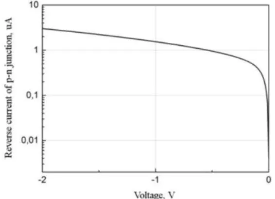
First of all interest was caused by the reverse bias of the diode characteristic, that determines reverse current, and standard dependence is given in a fig-ure 1.
Fig. 1 – The reverse bias characteristic of formed with PIII method p-n junction (measured on mesa structure)
3. RESULTS AND DISCUSSION
Usually for silicon structures with deep holes used Bosch-process of plasma-chemical etching, widespread for production of microelectromechanical and nanoelec-tromechanical systems (MEMS and NEMS).
It is based on two-step cyclic process of plasma etch-ing with a step of formetch-ing structure walls passivation and a step of its anisotropic etching. As a result, holes could be formed with a depth up to hundreds of microns in silicon. However, this method has some features, that can not always be combined with the requirements of micro- and nanoelectronics.
In particular, it is inevitable effect of scalloping walls, i.e. a type of roughness, which has a form of regu-lar circuregu-lar grooves. This disadvantage could be flat-tened by reducing the duration of steps; however, it is impossible to completely get rid of it. If one form p-n junction on such surface side, it would be inevitably
lead to increase the leakages in sharp places because of the field-effects.
The second feature is stubborn remnants of a thin polymer film in the holes (~ 1-3 nm). It polluting surface and has the potential opportunity to affect on the elec-trical characteristics of this structure. Therefore, in this research, we investigated the possibilities of another process, in particular the cryogenic process of deep plasma-chemical etching of silicon. Using of the cryo-genic etching permits to get the structures with high aspect ratio and smooth walls. This method permit to use a plasma SF6O2 without gases that produce a poly-mers (such as different freons) and without modulation plasma composition during the etching process.
In particular, low temperatures (from – 100 °C to – 130 °C) permit to eliminate the isotropic spontaneous etching of the structure sidewalls by atomic fluorine, which carry out with purely chemical isotropic mecha-nism. As the result, it has the Arrhenius temperature dependence. Besides, for the same reason that one can achieve high silicon etching selectivity relative to the rigid mask of photoresist or silicon dioxide. During etch-ing, oxygen formes protective coating composition SFxOy on the sidewalls, which prevents spontaneous etching by fluorine. The continuous process of cryogenic silicon etching is completely devoid of effect “scalloping”, that permits to get etching structure with a minimum roughness of the walls. In this paper, wall roughness after etching of silicon in сryoprocess was investigated by authors.
An additional advantage of this process is the poten-tial opportunity to permit managing etching profile (an-gle of inclination a wall). For etching on the specified depth is necessary apply highly selective lithographic mask. Use of a aluminum oxide mask was propossed. In the fluorine-containing plasma, the aluminium oxide forms non-volatile aluminum fluoride, which ensures high selectivity etching process.
Mask of aluminium oxide was deposited by atomic layer deposition method. As the organometallic precur-sor was used trimethylaluminium; as the oxidative pre-cursor was used oxygen plasma.
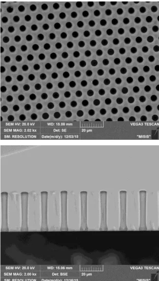
To product the structures was used templates for contact optical lithography with «honey comb» structure with 5 um holes in diameter. Deep etching performed with the chamber with cryogenic table through the mask of aluminium oxide with autopsied windows. The plate temperature was maintained at – 110 °С.
Firstly, the technological process was fine-tuned on etching holes, as it is easier to get a cross-section image. The etching result shows in an figure 2. The image shows that the obtained vertical walls have depth of 40 um, with a small positive angle of 89 deg., the size's offset does not exceed of 20 nm. The selectivity with a respect to the mask is better than 1 : 30000. The wall roughness study shows that this quantity is at most of the surface of the walls, with the exception of adjacent to a mask fields, and doesn’t exceeds the resolving pow-er of scanning electron microscope (SEM), i.e. it is in the range 1-3 nm.
PERSPECTIVE METHOD OF BETAVOLTAIC CONVERTER CREATION J.NANO-ELECTRON.PHYS. 8, 02022 (2016)
02022-3 Fig. 2 – Cross-section view of etched by cryogenic process holes
pattern is difficult to get a split, which perpendicular to the surface, and observe the etching profile without geometric distortion. However, carried out investiga-tions permit to estimate the depth of the etching, offset of the sizes and the verticality of hole's walls.
Further progress in the betavoltaic power source creation consist in practical realization of the formation of the radioactive 63Ni continuous layer on the inner surface of the holes. The process technology of not radi-oactive nickel deposition into the pores is known and described in detail [18].
4. CONCLUSION
Thus, the results obtained in p-n planar diode struc-ture, formed by plasma-immersion ion implantation
Fig. 3 – The structures of cylindrical holes, received with cryogenic etching (up view on the left, split - on the right)
process, by leakage are at the level of ~1 uA/cm2 at U – 1 V, which corresponds to the epitaxial planar junc-tions obtained by high-temperature CVD-methods. Au-thors developed a cryogenic process of plasma-chemical etching silicon, which permits to develop the structured silicon layer, with a system of deep holes (5 um in di-ameter) with a depth of 45 um. The silicon layer has the necessary parameters for creating a microstruc-tured 3D p-i-n junction with low reverse current. It permits to suggest, that made by PIII method p-n junc-tion with a wide deplejunc-tion area would be had leakages, acceptable for betavoltaic power source.
AKNOWLEDGEMENTS
K.V. RUDENKO,A.V. MIAKONKIH, ET. AL. J.NANO-ELECTRON.PHYS. 8, 02022 (2016)
02022-4 REFERENCES
1. V.N. Murashev, V.N. Mordkovich, S.A. Legotin, J. Nano-
Electron. Phys.6 No 4, 04012 (2014).
2. V.N. Murashev, S.A. Legotin, S.I. Didenko, Adv. Mat. Res. 1070-1072, 585 (2015).
3. A.A. Krasnov, S.A. Legotin, Yu.K. Omel’chenko, J. Nano-
Electron. Phys.7 No 4, 04004 (2015).
4. S.Yu. Yurchuk, S.A. Legotin, J. Nano- Electron. Phys. 7 No 3, 03014 (2015).
5. S.U. Urchuk, A.A. Krasnov, S.A. Legotin, J. Nano-
Elec-tron. Phys.7 No 4, 04005 (2015).
6. A.S. Korolchenko, S.A. Legotin, V.N. Murashev, M.N. Orlova, Metallurgist54 No 5-6, 328 (2010).
7. A.S. Korol'chenko, S.A. Legotin, S.I. Didenko, S.P. Kobeleva, Russ. Microelectron.40 No 8, 620 (2011). 8. V.N. Murashev, A.S. Korolchenko, S.A. Legotin,
Metallur-gist56 No 3-4, 303 (2012)
9. S.T. Revankar, T.E. Adams, J. Energ. Power Source 1 No 6, 321 (2014).
10.V.V. Starkov, S.A. Legotin, A.A. Krasnov, J. Nano-
Elec-tron. Phys.7 No 4, 04047 (2015).
11.George H. Miley, Nie Lou, 9th Annual International Ener-gy Conversion Engineering Conference (31 July - 03 Au-gust: San Diego, California: 2011).
12.Wei Sun, Nazir P. Kherani, Karl D. Hirschman, Larry L.
Adv. Mater. 1230-1233. (2005).
13.Kuan-Chih Huang, R. Dahala, James J.-Q. Lu, Y. Danon, I. B. Bhat. Proc. SPIE8710, 87101J (2013).
14.Kuan-Chih Huang, R. Dahala, James J.-Q. Lu, Y. Danon, I.B. Bhat. Appl. Phys. Lett.102, 152107 (2013).
15.Kuan-Chih Huang, R. Dahala, James J.-Q. Lu, A. Weltz, Y. Danon, I. B. Bhat, Nuclear Instrum. Method. Phys. Res. A. 763, 260 (2014).
16.Handbook on Plasma Immersion Ion Implantation and Deposition (Ed. by A. Anders) (Wiley: 2000).
17.I.S. Shahsenov, A.V. Miakonkikh, K.V. Rudenko, Proc. SPIE 9440, 94400Y (2014).
18.Chengkun Xu, Zhang Xi, King-Ning Tu, et al., J.