Study of the HVDC Dual Transmission System Under
Faults in the Power Converters
Natália M.R. Santos
INESC-ID Lisboa, Portugal ESTSetubal, Polytechnic Institute ofSetúbal, Portugal [email protected]
V. Fernão Pires
INESC-ID Lisboa, Portugal ESTSetubal, Polytechnic Institute ofSetúbal, Portugal [email protected]
J. Fernando Silva
INESC-ID, Instituto Superior Técnico, Universidade de Lisboa, Portugal [email protected]
Abstract— HVDC transmission systems based on voltage source converters have lately emerged as a good alternative to
conventional AC transmission. In these transmission systems multilevel converters have become a promising energy conversion technology. The reliability of the power converters are extremely important since a fault in these equipments may lead to an unavailability for a long period of the transmission system. Thus, this paper will focuses in HVDC dual transmission system under semiconductor failure conditions. As presented in this paper this structure presents interesting characteristics under the point of view the reliability considering a power semiconductor failure. It will present the consequences for the transmission system when there is a semiconductor fault. A study for the change of the modulation system in order to ensure DC link capacitors voltage balance under a fault condition is also presented. Simulation studies are shown in order to confirm the characteristics of the proposed methodology in normal and fault condition mode.
Keywords—HVDC transmission; Multilevel converter, Dual converter; Vectorial modulator; Semiconductor fault conditions.
I. INTRODUCTION
The HVDC transmission system has emerged as an attractive alternative to traditional AC transmission, due to its capability of transmitting large quantities of power over long distances. Also, can be seen as a useful solution to other problems of transport networks, such as network congestion, stabilization of power flows in integrated power systems and asynchronous connections of AC power systems [1-2].
At their beginning, HVDC transmission systems were based on current source converters (CSC) with line commuted thyristor, so called line commuted converters (LCC). This technology allowed that large amounts of power could be processed, however without full controllability of the system and with high harmonic contents.
The development and the availability of high rated fully controllable switches, such as the gate turn-off thyristor (GTO) and the insulated gate bipolar transistor (IGBT) contributed to the use of voltage source converter (VCS) as an attractive alternative to the CSC for HVDC systems [3].
In comparison with the classical HVDC systems, the VSC based HVDC offers a series of advantages such as, the ability to create a completely independent AC voltage waveform, the independent control of active and reactive power flow, the improvement of voltage stability and the increase of the transfer capability in AC systems [4-5].
The use of multilevel converters in HVDC systems, can be a suitable solution, to situations where are required higher voltage and power operation capability with lower voltage rating semiconductor devices, lower common-mode voltages, higher efficiency and reduced harmonic distortion is the use of multilevel converters.
Due to importance of the reliability of HVDC transmission systems, several studies have been presented. However, most of the studies have been focused on the AC and DC system faults [14-15]. Much less efforts have been made regarding a fault in the power converter switches. Thus, this paper analyses the operation of HVDC transmission systems based on the dual two-level converter topology, in normal and failure conditions of semiconductors. As will be presented, this topology presents interesting characteristics regarding fault tolerant operation under these fault types. It also is presented a study of the vector modulation that will ensure the capacitor voltage equalization for normal and failure conditions.
II. HVDCMULTILEVEL BASED ON DUAL TWO LEVEL CONVERTER
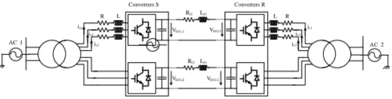
The HVDC transmission system that will be studied is presented in Fig.1. It consists of the two standard three-phase two level voltage source converters connected to AC sides by a three phase transformer with the secondary in the open end configuration. The DC link capacitor provides the necessary DC voltage for the dynamics of the system and offers filtering for the DC harmonics.
RO LO
R L
is1 is2
is3 AC 1
RO LO
VD Cs1
Converters S Converters R
VD Cs2 VD Cr2
VD Cr1 ir1
ir2
ir3 AC 2
R L
Fig. 1. Diagram configuration of the HVDC based on dual two level converter.
In the dual two-level converter topology (Fig. 2) the several series connected IGBTs are used for each semiconductor to support a high blocking voltage capability and consequently increase the DC bus voltage level of the HVDC system.
i01
i1DC
S11 S12 S13
S’11 S’12 S’13
V11
V12
V13
iC1
S21 S22 S23
S’21 S’22 S’23
V21
V22
V23
i2DC
iC2
R L
i1
R L
R L
VDC2
VDC1 i2
i3
i02
V2
V1
V3
Vs1
Vs2
Vs3
Fig. 2. Circuit diagram of the dual two-level converter.
To obtain the dual converter model, ideal power switches will be considered. So, in accordance with Fig. 2, the time dependent variable k(t) with k{1,2,3} which represents the states of the switches, can be expressed by (1).
ON i 2 OFF i 1 if 0
OFF i 2 ON i 1 if 1 ) (
s k S s
k S
s k S s
k S t
k
(1)
The AC output voltages at each of the converters are function of the power semiconductors state and DC voltage sources, as expressed by equation (2).
2
23 22 21
1
13 12 11
3 2 1
3 2 3 1 3
1 3
1 3 2 3
1 3
1 3 1 3 2
3 2 3 1 3
1 3
1 3 2 3
1 3
1 3 1 3 2
DC
DC V
V V
V V
In the α,β plane, the AC output voltages can be obtained using the Clarke-Concordia matrix transformation, through the following relationship [16]:
2 23 22 21 1 13 12 11 2 3 2 3 0 2 1 2 1 1 3 2 2 3 2 3 0 2 1 2 1 1 3 2 DC DC V V V V (3)
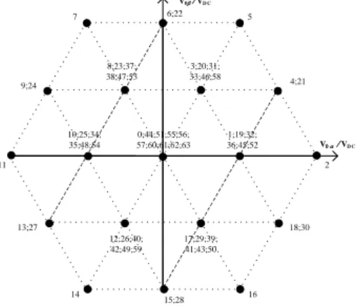
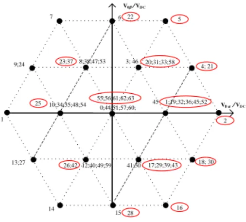
From the relation (3) and according to all the switching states, it is possible to verify that 64 different output voltage levels can be obtained. However, bearing in mind that DC voltages of the converters are equal (VDC1=VDC2), it will be achieved 19 different output voltage vectors (Fig. 3). The other vectors are redundant and will be used to capacitor voltage balance.
V0 / VD C 4;21 2 16 14 7 15;28 1;19;32; 36;45;52 3;20;31; 33;46;58 0;44;51;55;56; 57;60;61;62;63 17;29;39; 41;43;50 18;30 12;26;40; 42;49;59 13;27 11 10;25;34; 35;48;54 9;24 8;23;37; 38;47;53
V0 / VD C
5 6;22
Fig. 3. Output voltage vectors of the three-phase dual two-level converter, in , frame.
The state space model of the dual converter in three phase reference frame and dq frame, will be necessary to study the HVDC system controller. Then, applying the dq transformation and considering VDC1=VDC2=VDC, leads to:
sq sd q d DC DC q d DC DC q d q d V V L L L V L V L V L V i i L R L R i i dt d 1 0 0 1 0 0 0 0 0 0 2 2 1 1 (4)
The system controller is developed in order to control the active and reactive power that flows into the HVDC transmission system, as well accomplish the DC link voltage regulation. The active power P and reactive power Q in dq coordinates, can be expressed as: q d sd sq sq sd i i V V V V Q P (5)
Whereas that the three phase source voltages are balanced, which means that Vsq=0, the following relation can be obtained:
q sd d sd i V Q i V P (6)
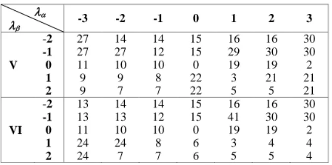
One of the problems of this structure is the regulation and balance of the voltages in both DC capacitors. This will be made through the use of a voltage vector modulation. Thus, from the analysis of the circuit (Fig. 2) it is possible to verify that from the 64 vectors only 19 define 19 distinct output voltage vectors (Fig. 3). The extra ones are redundant, but will be used to equalize and balance the two DC capacitors voltage. However, the choice of the appropriate voltage vectors implies to know the location of the AC currents. Thus, six sectors will be considered in accordance with Fig. 4. The voltage vectors will be reached through a five level and seven level hysteretic comparators. The outputs of these comparators are the variables {-2;-1;0;1;2} and {-3;-2;-1;0;1;2;3} corresponding to five and seven selectable levels, respectively. According to this and taking in account the switching combination scheme (Fig. 5), the voltage vector selection will be done using Tables I and II, in accordance with the outputs of the histeretic comparators and the DC capacitor voltage equalization.
Imax
Imax
III II
I IV V VI
i1 i2 i3
Fig. 4. AC currents and resulting sectors.
TABLE
I
1 1
2
2
VD C1> VD C2
VD C1< VD C2
S11 .. S23
i1
i2
i3
TABLE
II
Fig. 5. The switching combination scheme.
TABLE I. WITCHING TABLE FOR VDC1> VDC2,SHOWING VECTOR SELECTION UPON THE VARIABLES AND FOR NORMAL OPERATION
-3 -2 -1 0 1 2 3
I -2 -1 0 1 2
13 13 11 24 24
14 13 34 24 7
14 12 34 23 7
15 15 0 22 22
16 17 1 31
5 16 30 1 4 5
30 30 2 4 4
II -2 -1 0 1 2
13 13 11 9 9
14 13 25 9 7
14 42 25 23 7
28 28 0 22 22
16 17 32 31 5
16 18 32 4 5
30 30 2 4 4
III -2 -1 0 1 2
13 13 11 9 9
14 13 25 9 7
14 26 25 37 7
28 28 0 22 22
16 43 32 31 5
16 18 32 4 5
18 18 2 4 4
IV -2 -1 0 1 2
27 27 11 9 9
14 27 35 9 7
14 26 35 8 7
15 15 0 22 22
16 29 36 31 5
16 18 36 4 5
-3 -2 -1 0 1 2 3
V -2 -1 0 1 2 27 27 11 9 9 14 27 10 9 7 14 12 10 8 7 15 15 0 22 22 16 29 19 3 5 16 30 19 21 5 30 30 2 21 21 VI -2 -1 0 1 2 13 13 11 24 24 14 13 10 24 7 14 12 10 8 7 15 15 0 6 6 16 41 19 3 5 16 30 19 4 5 30 30 2 4 4
TABLE II. SWITCHING TABLE FOR VDC1< VDC2,SHOWING VECTOR SELECTION UPON THE VARIABLES AND FOR NORMAL OPERATION
-3 -2 -1 0 1 2 3
I -2 -1 0 1 2 27 27 11 9 9 14 27 35 9 7 14 26 35 8 7 28 28 0 6 6 16 19 36 33 21 16 18 36 21 21 18 18 2 21 21 II -2 -1 0 1 2 27 27 11 24 24 14 27 10 24 7 14 40 10 8 7 15 15 0 6 6 16 29 19 3 5 16 30 19 21 5 30 30 2 21 21 III -2 -1 0 1 2 27 27 11 24 24 14 27 10 24 7 14 12 10 23 7 15 15 0 6 6 16 41 19 20 5 16 30 19 21 5 30 30 2 21 21 IV -2 -1 0 1 2 13 13 11 24 24 14 13 34 24 7 14 12 34 23 7 28 28 0 6 6 16 17 1 20 5 16 30 1 21 5 30 30 2 4 4 V -2 -1 0 1 2 13 13 11 24 24 14 13 25 24 7 14 42 25 23 7 28 28 0 6 6 16 17 32 31 5 16 18 32 4 5 18 18 2 4 4 VI -2 -1 0 1 2 27 27 11 9 9 14 27 25 38 7 14 26 10 8 7 28 28 0 22 22 16 43 32 31 5 16 18 32 21 5 18 18 2 21 21
III. HVDC IN FAULT CONDITIONS
V0 / VD C
14 7
15 41;50 13;27
11
10;34;35;48;54 9;24
V0 / VD C
6
3; 46
4; 21
18; 30
16
22 5
2 20;31;33;58
45 1;19;32;36;45;52
28 17;29;39;43 12;40;49;59
26;42 25
0;44;51;57;60; 55;56;61;62;63 8;38;47;53 23;37
Fig. 6. Output voltage vectors of the dual converter with S11 in fault condition.
Since several unavailable voltage vectors were used in the modulation strategy for the normal condition (tables I and II), a change in the choice of the vectors should be made. As an example, it will be presented the impact on the tables related with sector I. In this case the new vectors that must be chosen are presented in tables III and IV.
TABLE III. SWITCHING TABLE FOR VDC1> VDC2,SHOWING VECTOR SELECTION UPON THE VARIABLES AND FOR OPEN SWITCH S11.
-3 -2 -1 0 1 2 3
-2 -1 0 1 2
13 13 11 24 24
14 13 34 24 7
14 12 34 47 7
15 15 0 6 6
15 50 45 46 6
15 50 45 46 6
50 50 45 46 46
TABLE IV. SWITCHING TABLE FOR VDC1< VDC2,SHOWING VECTOR SELECTION UPON THE VARIABLES AND FOR OPEN SWITCH S11.
-3 -2 -1 0 1 2 3
-2 -1 0 1 2
27 27 11 9 9
14 27 35 9 7
14 40 35 8 7
15 15 0 6 6
15 41 45 3 6
15 41 45 3 6
41 41 45 3 3
IV. RESULTS IN NORMAL AND FAULT CONDITIONS
The proposed HVDC structure based on dual two level converter and their control system, in normal and faulty operation, have been carried out by several simulations using the software Matlab/Simuling/Power System Blockset. The presented results were obtained with the HVDC system connected to a grid through two power transformers (132/78.5 kV, 110/78.5 kV) with 70 MVA each.
2.9 2.92 2.94 2.96 2.98 3 3.02 3.04 3.06 3.08 3.1 -1000
-800 -600 -400 -200 0 200 400 600 800 1000
Time [s]
C
u
rr
e
n
ts
[A
]
i1 i2 i3
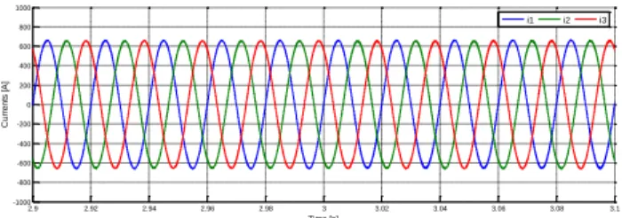
Fig. 7. Three-phase AC line currents of the HVDC converter S.
2.5 2.6 2.7 2.8 2.9 3 3.1 3.2 3.3 3.4 3.5
3.48 3.485 3.49 3.495 3.5 3.505 3.51 3.515 3.52x 10
4
Time [s]
V
o
lt
a
g
e
[
V
]
VDC1
Fig. 8. Voltage waveform of capacitor VDC1 of the HVDC converter S.
2.5 2.6 2.7 2.8 2.9 3 3.1 3.2 3.3 3.4 3.5
3.48 3.485 3.49 3.495 3.5 3.505 3.51 3.515 3.52x 10
4
Time [s]
V
o
lt
a
g
e
[
s]
VDC2
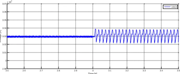
Fig. 9. Voltage waveform of capacitor VDC2 of the HVDC converter S.
2.5 2.6 2.7 2.8 2.9 3 3.1 3.2 3.3 3.4 3.5
3.145 3.15 3.155 3.16 3.165 3.17 3.175 3.18 3.185x 10
4
Time [s]
V
o
lt
a
g
e
[
V
]
VDC1
Fig. 10.Voltage waveform of capacitor VDC1 of the HVDC converter R.
2.5 2.6 2.7 2.8 2.9 3 3.1 3.2 3.3 3.4 3.5
3.145 3.15 3.155 3.16 3.165 3.17 3.175 3.18 3.185x 10
4
Time [t]
V
o
lt
a
g
e
[
V
]
VDC2
Fig. 11.Voltage waveform of capacitor VDC2 of the HVDC converter R.
2.9 2.92 2.94 2.96 2.98 3 3.02 3.04 3.06 3.08 3.1 -1000
-800 -600 -400 -200 0 200 400 600 800 1000
Time [s]
C
u
rr
e
n
ts
[A
]
i1 i2 i3
Fig. 12.Three-phase AC line currents of the HVDC converter R.
2.5 2.6 2.7 2.8 2.9 3 3.1 3.2 3.3 3.4 3.5
3.145 3.15 3.155 3.16 3.165 3.17 3.175 3.18 3.185x 10
4
Time [s]
V
ol
ta
ge
[V
]
VDC1
Fig. 13.Voltage waveform of capacitor VDC1 of the HVDC converter R.
2.5 2.6 2.7 2.8 2.9 3 3.1 3.2 3.3 3.4 3.5
3.145 3.15 3.155 3.16 3.165 3.17 3.175 3.18 3.185x 10
4
Time [s]
V
ol
ta
ge
[V
]
VDC2
Fig. 14.Voltage waveform of capacitor VDC2 of the HVDC converter R.
2.9 2.92 2.94 2.96 2.98 3 3.02 3.04 3.06 3.08 3.1
-1000 -800 -600 -400 -200 0 200 400 600 800 1000
Time [s]
C
u
rr
e
n
ts
[A
]
i1 i2 i3
Fig. 15.Three-phase AC line currents of the HVDC converter R.
2.5 2.6 2.7 2.8 2.9 3 3.1 3.2 3.3 3.4 3.5
2.99 3 3.01 3.02 3.03 3.04 3.05 3.06 3.07x 10
4
Time [s]
V
o
lt
a
g
e
[
V
]
VDC1
2.5 2.6 2.7 2.8 2.9 3 3.1 3.2 3.3 3.4 3.5 2.99
3 3.01 3.02 3.03 3.04 3.05 3.06 3.07x 10
4
Time [s]
V
o
lt
a
g
e
[
V
]
VDC2
Fig. 17.Voltage waveform of capacitor VDC2 of the HVDC converter R.
V. CONCLUSIONS
The analysis of a HVDC transmission system based on the dual two-level converter topology under normal and fault conditions operation has been presented. This HVDC transmission system is characterized by two three phase converters with AC terminals connected to a three phase transformer with the open winding configuration. Besides the simple structure this system is characterized by its capability to fault tolerant operation under a semiconductor failure. The system is controlled by a voltage sliding mode controller associated to a vector modulator. It ensures the active and reactive power to their reference values and regulate the DC link of each converter. The vector modulator was designed in order to achieve the balance of the DC capacitors. To reach the fault operation conditions a change of the switching tables used in the vector modulator selection were proposed. This change ensures operation under fault operation conditions, the AC currents maintaining lower distortion and the DC voltage capacitors still keeping their balance. Simulation results have been presented in order to verify the characteristics of the proposed HVDC system under switch fault condition.
ACKNOWLEDGMENT
This work was supported by national funds through Instituto Politécnico de Setúbal and Fundação para a Ciência e a Tecnologia (FCT) with reference UID/CEC/50021/2013.
REFERENCES
[1] V. G. Agelidis, G. D. Demetriades and N. Flourentzou, “Recent advances in high-voltage direct-current power transmission systems,” Proc. IEEE Int. Conf.
Ind. Technol. (ICIT 2006), pp. 206-213.
[2] J. Arrillaga, Y. H. Liu and N. R. Watson, Flexible Power Transmission: The HVDC Options. Chichester, U.K.: Wiley, 2007.
[3] K. Friedrich,, “Modern HVDC PLUS Application of VSC in Modular Multilevel Converter Topology,” IEEE International Symposium on Industrial
Electronics (ISIE), pp. 3807-3810, 2010.
[4] N. Flourentzou, V. G. Agelidis and G. D. Demetriades, “VSC-Based HVDC Power Transmission Systems: An Overview”, IEEE Trans. on Power
Electronics, vol. 24, nº 3, pp. 592-602, 2009.
[5] C. Du, E. Agneholm, and G. Olsson, “Use of VSC-HVDC for industrial systems having onsite generation with frequency control”, IEEE Trans.on Power
Delivery, vol.23, nº 4, pp.2233-2240, 2008.
[6] U. M. Choi, H. H. Lee, and K. B. Lee, “Simple Neutral-Point Voltage Control for Three-Level Inverters Using a Discontinuous Pulse Width Modulation”,
IEEE Transactions on Energy Conversion, Vol. 28, nº 2, pp.434-443, 2013.
[7] N. M. R. Santos, V. F. Pires and J. F. Silva, “Fault Tolerant Operation of Active Neutral Point Clamped Multilevel Converters Using a Voltage Slinding
Mode Controller”, PEMC 2014, pp. 1072-1077, 2014.
[8] V.G. Agelidis and L. Xu, “A novel HVDC system based on flying capacitor multilevel PWM converters”, Proceedings of CIGRE International Conference
on Power Systems, 2001.
[9] C. Feng, J. Liang and V.G. Agelidis, “Modified phase-shifted PWM control for flying capacitor multilevel converters”, IEEE Trans. Power Electron., vol.
22, nº 1, pp.178-185, 2007.
[10] P. C. Loh, D.G. Holmes, T.A. Lipo, “Implementation and control of distributed PWM cascaded multilevel inverters with minimal harmonic distortion and
common-mode voltage”, IEEE Trans. Power Electro. vol. 20, nº 1, pp.90-99, 2005.
[11] R. Marquardt, A. Lesnicar, “New Concept for High Voltage Modular Multilevel Converter”, PESC 2004, Conference in Aachen, Germany.
[12] D. Soto-Sanchez and T. C. Green, “Control of a modular multilevel converter based HVDC transmission system”, 14th European conference on power
electronics and applications (EPE 2011), p. 1-10, 2011.
[13] D Casadei, G. Grandi, A. Lega and C. Rossi, “Multilevel Operation and Input Power Balancing for a Dual Two-Level Inverter with Insulated DC Sources”,
IEEE Trans. on Industry Applications, vol. 44, nº 6, pp.1815-1824, 2008.
[14] Y. Zhang, N. Tai and B. Xu, “Fault Analysis and Traveling-Wave Protection Scheme for Bipolar HVDC Lines”, IEEE Trans.on Power Delivery, vol.27, nº
3, pp.1583-1591, 2012.
[15] J. Rafferty, L. Xu and D. J. Morrow, “DC Fault Analysis of VSC Based Multi-terminal HVDC Systems”, 10th IET International Conference on AC DC
[16] J. F. Silva, “Control Methods for Power Converters”, chapter 19 of the “Power Electronics Handbook”, Editor M. H. Rashid, Academic Press, USA, 2001. [17] V. F. Pires, J. Fialho, J. F. Silva, “HVDC transmission system using multilevel power converters based on dual three-phase two-level inverters”,
International Journal of Electrical Power and Energy Systems, vol. 65, pp 191–200, 2015.
[18] J. Suonan, S. Gao, G. Song and Z. Jiao, “A Novel Fault-Location for HVDC Transmission Lines”, IEEE Trans.on Power Delivery, vol.25, nº 2,
pp.1203-1209, 2009.
[19] J. Yang, J. E. Fletcher and J. O’Reilly, “Short-Circuit and Ground Fault Analyses and Location in VSC-Based DC Network Cables”, IEEE Trans. on
Industrial Electronics, vol. 59, nº 10, pp. 3827-3837, 2011.
[20] L. Yan, S. Wei, C. Yong-ning, W.Lin-jun and L. Wei, “Research on Offshore Wind Farm VSC-HVDC Transmission System Fault Ride Through Issue”,