Influence of Parasitic Capacitances in Modeling
and Analysis of Advanced Floating Gate Memory
Devices
Andre Moreira", Jose Machado da Silva" and Guoquiao Tao",IEEEsenior member a: Universidade do Porto, Rua Dr. Roberto Frias, 4200-265 Porto , Portug al
b:NXP Semiconductors, Gerstweg 2, 6534 AE Nijmegen, the Netherlands Phone: (+31) 24 3534549 Email: Guoqiao .Tao@nxp .com
Abstract-In this paper, we report the impact of the parasitic capacitances in the modeling and analysis of advanced floating gate (FG) non-volatile memory (NVM) devices, especially on the coupling ratio. Due to the poor accuracy of the existing capacitance model when compared to practice, an approach to include the parasitic capacitances has been established. Measurement results from two transistor (2T) Fowler-Nordheim (FN) tunneling operated flash memory show a good improvement in the model accuracy. The parasitic capacitances depend very much on the floating gate dimension, and the spacing to the neighboring elements in the flash cell array. The growing influence of the parasitic capacitances and the subsequent degradation of the existing model accuracy can be expected for the cells dimensions in future process technologies. With the accurate calculation method for the parasitic capacitances proposed in this paper, the cell characteristics can be more accurately modeled, and the degradation of the cell can be accurately studied.
I. INTRODUCTION
The Non-Volatile memory (NVM) sector today occupies one
of the largest portions of semiconductor market , with
application areas like portable storage/data-transport, digital camera/video storage , and storage medium for media players .
Technology-wise, it has become a driving force for
semiconductor technology scaling. NVM devices have also been successfully implemented in embedded systems (like system on chip, SOC), for application areas like e-passports , smart-cards, and micro-controllers. These application areas with embedded NVM have very high requirements on reliability. A high reliability requires a good understanding and accurate modeling of the device right from the development phase.
This paper addresses accurate modeling of the capacitances and coupling ratio (basic but very important parameters) in floating-gate based NVM devices. We report that the parasitic capacitances are becoming more and more important in technology scaling, and that they can be easily modeled in an accurate way. Furthermore, since the floating gate size increasing is a technique widely used by engineers to increase cell coupling ratios, the influence of the floating gate dimensions in these capacitive parameters (for the same technology node) is also studied and reported.
The calculations are applied to a 2T-FNFN-NOR device from
a state-of-the-art technology [1], being verified with
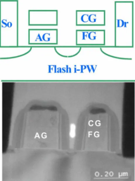
experimental data obtained from a large amount of memory cells, to avoid cell-to-cell variation effects . Fig. 1 shows the schematics and transmission electron microscopy (TEM) cross-section of such a 2T-FNFN-NOR device .
Flashi-PW
Fig.I .Top: A schematic cross section of the two-transistor cell. Control gate (CG) and floating gate (FG) are on the right side near the drain (Dr) while the access gate (AG) is on the left side near the source (So). Bottom: TEM cross-section of the two-transistor cell in 90nm node.
II. MODELS
Although a 2T-FNFN-NOR device has been used as a concrete example in our calculations, the method being proposed is applicable to other NVM floating gate devices .
Fig. 2 shows a 3-D drawing of the cell with channel, floating gate (FG) and access gate (AG). The control gate (CG) is not drawn to simplify the view.
A. Simplified Capacitance Model
J
ox=
a-E~x .(exp(-f3/
Eox)) (1)IVox
IE
=
KCG.(VCG -~
+
~n)
+
Vjb (3)IVoxlp
=K
CG '(VCG-~
+~n)
(4)where ~ is the threshold voltage of the cell, ~n is the threshold voltage when there is no charge stored in the FG, Vjbis the flat band voltage and KCG is the coupling ratio that denotes the
fraction ofVCGwhich will appear across the tunnel oxide .KCG
can be obtained from the various capacitances in the cell as:
(7)
10+1
C
r:::!f
e . eo .
Wdl'
e·/'
10
Nl~
channelFig. 2. Schematic geometry of a 2T-FNFN-NOR memory cell. The stacked CG above FG is omitted in the drawing . The bit line (BL) corresponds to the cell 's drain. Cell's dimensions indicated in black and parasiti c capacitances in green and blue . Capacitances labeled with the same number are symmetrical and have the same value.
Calculating fringe capacitances without using
finite-element-methods (FEM) requires a correct formulation for the capacitance between non-parallel plates. Fig. 3 shows a schematic of a capacitor with two plates with the same areaw .I,
oriented with angle
e
in theI 'direction, and with a distance10from the origin(0)to the plate edge. Assuming that the electric field lines are semi-circular and considering (6) for an infinitesimal area section w·dl" the capacitance between the two plates can be obtained by solving the integral:
(5)
K
-
C
1PDCG
-C
1PD+
Cox
where Eoxis the electric field across the oxide, andaand pare tunneling constants. Eoxis given by :
s.;
=
IVoxI
(2)tox
where Voxis the voltage drop across the oxide and toxis its thickness. For a certain amount of charge stored in the FG, Vox can be expressed for program and erase operations
(I
Voxlp,1VoxlE),as a function of the applied potential in the CG(VCG) ,in
terms of a simple coupling ratio:
where CIPD is the inter-poly dielectric capacitance, i.e. the
capacitance between FG and CG, and Coxis the tunnel oxide capacitance, i.e. the capacitance between FG and the channel. These capacitances are approximately calculated using a parallel plate capacitor model and neglecting any fringe or parasitical capacitance, which leads to:
B. The modified model including parasitic capacitances where eis the dielectric permittivity, eois the empty space permittivity, A is the plates ' area and d the distance between them.
The approximation as described in equation (6) worked pretty well in old technologies (down to sub-micrometer node) [3], but
became inaccurate since the technology entered the
deep-sub-micrometer era, due to the existence of many non-negligible parasitic capacitances in the cell.
To estimate these parasitic capacitances we split the cell's geometry in small parts that can be approached by parallel, orthogonal, or in line configurations. Fig. 2, schematically shows such various fringe/parasitic capacitances in a typical 2T-FNFN-NOR memory cell with a classic bar form FG.
(8)
J'
I
o...- -...---I~
C
r:::!e· eo .
w}J
1
+
1
0 )e
11
1
0Fig. 3. Schematic of a capacitor with non-parallel plates in thel'direction . This model is used for the analytic calculation of the fringe capacitances .
Special attention needs to be paid to the permittivity of the different dielectric materials (e) in the fringe/parasitic capacitors.
After considering the parasitic capacitances, the coupling ratio formula becomes:
which leads to: (6)
e-e
·A
C=
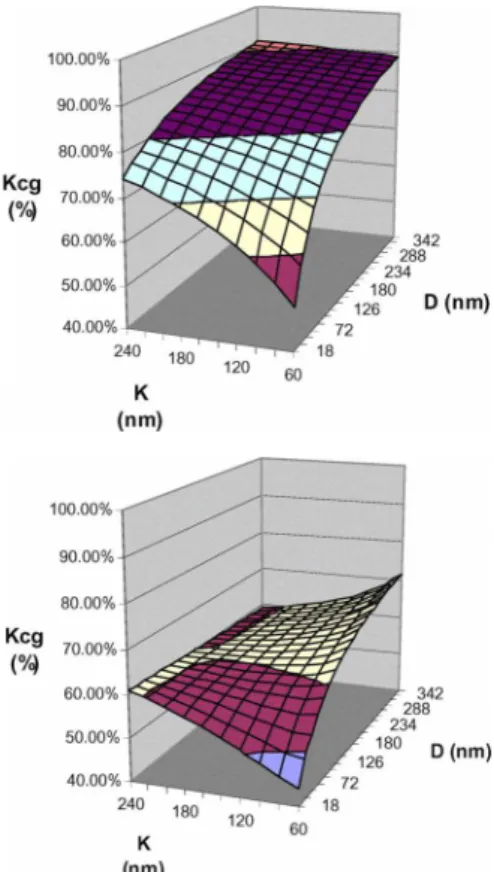
0Fig. 4. Dependence ofKCGwith theDandKdimensions of the FG. Top :
traditional model. Bottom : model taking into account the parasitic capacitances.
C IPD +Cjg-eg,p
KCG
=
(9)C IPD
+
C
jg-cg ,p+
Cox+
C
fg-rrest.po(nm)
120 ~O
Measurements have been carried out on 2.7Mbit arrays of devices fabricated in 90nm embedded NVM technology during development phase, and the median results for the array population were considered in order to avoid cell-to-cell variation effects.
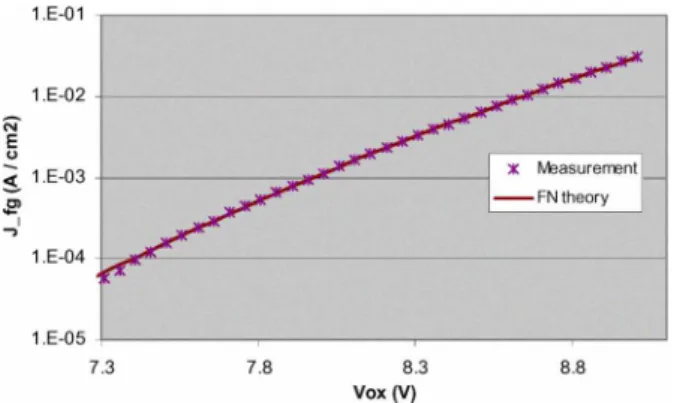
First, gate current density measurements (JG-VG) were
performed on a FG directly connected array. These
measurements prove that the measured gate current is governed by the FN equation, with values foraand
f3
in accordance to the ones reported by Kolodny [5]. Fig. 6 shows the measured.Zj-E, curve and the best-obtained fit with the FN equation.In a FG cell (FG really floating), the tunneling current can be extracted from program/erase speed measurements, i.e. the threshold voltage change in time [1-3], ifKCG and C/PD are
known.
As shown in the graph of fig. 7, a large error exists (between the calculated and measuredJ G-VGcurves) ifKCGand CIPDare
calculated without including the parasitic capacitances. In contrast, when taking into account the parasitic capacitances to determineKcG,an excellent agreement can be obtained.
III.EXPERIMENTAL VALIDATION
K (nm)
Fig. 5. Relative error introduced inKCGcalculation by neglecting the parasitic
capacitances.
10.00%
30.00%
-Keg 25.00%
Relative 2o .00 % 'I1 71 '11 '-:fi. ~ .x\
Error
( "I~ 15 00%
compensated by the smaller increase of the parasitical
capacitance l' added to the normal increase ofC/PD.
Thus, the point where KCG is maximum, is no longer for
maximumKandDbut actually for maximumDand minimum
K.
Fig. 5 plots the relative error introduced by using the simplified capacitance model. It makes clear that the error is higher as both FG dimensions increase, which means a much smallerKCGvalue than expected from the simple model.
Since increasing the FG dimensions is a common practice to increase KcG, the previous result shows that special attention
should be paid to the parasitic capacitances when performing this operation, in order to obtain an actually higherKCG.
35.00%
100.00%
90 .00 % 80.00% Keg
70.00 %
( O /~
D(nm)
120 60 K
(nm)
100.00%
-
--90.00%
Keg 70.00 %
(O /~
60.00%
o (nm)
120 60 K
(nm)
From Fig. 4 one concludes that increasing the FG height and width will increase the coupling ratio, but only till a certain point, after which increasing these dimensions will cause almost no raise or even a drop on the coupling ratio. E.g . for a FG D above 100 nm, the increase of the FGK,has almost no effect on the coupling ratio, actually causing it to decrease specially when K is still close to the channel width. This happens due to a big raise of the parasitic capacitances 2 and 5 (see fig. 2) when we
start raising K, which in the case of a high FG D, is not
where Cjg.cg,pis the total parasitic capacitance between FG and
CG (represented by the blue capacitances in fig . 2), and
Cjg.resl,pis the total parasitic capacitance from FG to all the rest
nodes (represented by the green capacitances in fig . 2) .
For this cell, the traditional capacitance model predicts
Kco=83.9%, while the model including the parasitic capacitances predictsKCG=71.4%. Note that the gate currents in
fig. 6, fig.7 and fig. 8 where extracted from measurements on cell structures from the same wafer to avoid issues caused by process variations .
1.E-01 ·r -- - - ---,
1.E-02+-- - - - - - - - - - - ___.ro'""'-- - ____;
N
E o
~ 1.E-0 3+ - - - -._--=---1 .g>
I
..,
1.E-04 .t-...c"'- - - ____;
IV.DISCUSSIONS
22nm 180nm 90 nm 45nm
Technology 360nm
---:::
---
____ without ---parasitics -+- with parasitics '<,-.
-,
100.00% 95.00% 90.00% 85.00% ;; 80.00% OJ lJ 75.00% l<: 70.00% 65.00% 60.00% 55.00%As described above, for the 90nm technology node cell used in our measurements, KCG can be simply about 14.9% (relative
error) lower than expected when the parasitic capacitances are neglected. When moving the same cell for a 45nm technology, the traditional model predictsKcG=89.1%, an absolute increase
of 5.2% (due to a strong reduction of the capacitance Cox) compared to the 90nm technology . However, when looking to the model including the parasitic capacitances, KcG=67.4% is
obtained, actually leading to an absolute KCG decrease of 4%
when compared to the 90nm technology. Thus, the relative error introduced in the KCG calculation by using the simplified
capacitor model in a 45nm technology, will increase to 24.3% and it will keep increasing as we downscale the technology.
Fig.9 shows the evolution ofKCG for the same kind of cell
used in our measurements, built in different technology nodes (downscaling the horizontal dimensions) . As we can see, the error is higher for smaller technologies, besides it is clear that when considering the parasitic capacitances for technologies bellow 180nm,KCGwill actually decrease as we downscale the
cell, in opposition to the prediction obtained neglecting these parasitic capacitances.
Fig. 9.KeGevolution with technology downscaling . Values obtained for the same cell used in our measurements, downscaling all the horizontal dimensions.
8.5 7 7 .5
Vo x (V)
6.5
-
--_ -c---,-->
,...-;
->
.>
/
~1/
/
x
M easurem ent. /
- FN ca lculated withxv?
- - parasiticsFN ca lculated woV parasitics
1.E-Q8 1.E-Q9
5.5 1.E-Q7
Fig. 7. Measured gate current density and respective fit with the FN equation for fresh cells . FN approximation obtained with and without considering the
parasitic capacitances and V",=O.806 V.
N
S
1 E-05 1 - - - , . - -£ ' ' - - - 1<
~ 1.E-06 l---~
....
~~- _____j i"': ~=~ ::;; , I..,
1.E-04 1---- - - ----..",,- - - ----1 1.E-03 1---- - - -,/"--- ---1
1.E-07 1-- - - -/ '--- - - - ---'==========:.---1
1.E-Q1 1.E-Q2 1.E+OO
The data shown in fig. 7 were obtained from an un-stressed (thus fresh) cell with a classic bar form FG, considering for the FN approximation theaand
p
values obtained from theJG-VGmeasurement and a standard Vtnfor an uncycled cell of 0.806 V.
When considering a stressed cell with lOOK program/erase cycles, the fit is still very accurate as shown in fig. 8. This fit for the cycled cell was obtained with V,n=1.46V,which shows av'n
degradation of 0.654 V compared to the fresh cell.
1.E-0 5.f--- - - - ,.--- - - ---,- - - - ----,- - ----'
7.3 7 .8 8 .3 8 .8
Vox (V)
Fig. 6. Gate current density measured with the potential directly applied to the FG. Fitting with the FN equation obtained with a=I .23E-05 A1V2and
,8=2.60E+lOVim,and consideringVjb=O.992V.
N 1.E-Q3
E
~ 1.E-Q4
~ 1.E-Q5
~ I 1.E-Q6
1.E-08 .L'/• •~ ____;
In addition, the parasitic capacitances can affect the performance of the cell, lowering the coupling ratio and causing extra stress in some of the cell's components, as coupling ratios above 70% are very important to keep the program/erase
potentials in a low value, to avoid damage on the
oxide-nitride-oxide (ONO) layer and to maximize the cell's window. Therefore , these parasitic capacitances need to be minimized in future technologies.
9
8 .5
8 7 Vox (V{-5 6 .5
6 1.E-09 -'-.----.----r---,---,---~r---,---I
5.5
Fig. 8. Measured gate current density and respective fit with the FN equation for cells stressed with lOOK program/erase cycles . FN approximation obtained taking into account the parasitic capacitances and considering V",=1.46 V, a=2 .5E-06 A/V2
Note also, that the coupling ratio and the tunneling constantsa
and{3,are not symmetric for program and for erase operations. In this paper, the Keg values as well as the JG-VG curves, are
obtained for the erase operation. Nevertheless, during the execution of this work, the same process has been applied to the program operation and the results are in close agreement with the ones being published here.
V.CONCLUSIONS
When the parasitic capacitances are neglected, the simple model proposed by Kolodny [5] can no more describe the
floating-gate cell characteristics in deep-sub-micrometer
technologies, although the physics stays the same. Extending the usage of the Kolodny model requires an accurate calculation of the coupling ratio by including the parasitic capacitances
Cjg-cg,p and Cjg-rest,p in the cell. This paper shows how these
parasitic capacitances can affect theKCGcalculations.
We conclude that for an 180nm technology node, the parasitic capacitances already cause a significant KCG lowering, which becomes stronger for the current small dimension technologies. It is also shown that, the importance of these parasitic capacitances increase even more as we tryto increaseKCGby
increasing the FG size. It is therefore imperative to include them in the KCG calculations for current and especially for future
technologies.
With the accurate calculation method for the parasitic capacitances proposed in this paper, the cell characteristics can be more accurately modeled, and the degradation of the cell can be accurately studied.
REFERENCES
[1] G. Tao, et al. "A Low Voltage, Low Power, High Reliable,
Multi-Purpose, Cost-Competitive Embedded Non-Volatile
Memory in 90nm Node", 2nd International Conference on Memory Technology and Design (ICMTD), pp 113-115, 2007. [2] G. Tao, et al., "A simple and Accurate Method to Extract Neutral Threshold Voltage on Floating Gate Flash Devices and Its Application to Flash Reliability Characterization", in IEEE International Integrated Reliability Workshop (IRW) Final Report, pp 52 - 56, 2007.
[3] S. Satoh, et al., "Stress-Induced Leakage Current of Tunnel
Oxide Derived from Flash Memory Read-Disturb
Characteristics", in IEEE Transaction on Electron Devices, Vol. 45, No.2, pp 482-486, 1998.
[4] G. Tao, "Reliability of Advanced Embedded Non-Volatile Memories: The 2T-FNFN Device", in ICICDT proceedings, 2008.
[5] A. Kolodny, et al. "Analysis and Modeling of Floating-Gate EEPROM Cells", in IEEE Transaction on Electron Devices, Vol. 33, No.6, pp 835-844, 1986.
[6] G. Tao, et al, "Characterization and Modeling of
Program/Erase Induced Device Degradation in 2T-FNFN-NOR Flash Memories", in Proceedings of the 15th IEEE International Symposium on the Physical and Failure Analysis of Integrated Circuits (IPFA), 2008.
[7] W. D. Brown, J. E. Brewer, "Nonvolatile Semiconductor