Bruno João Baptista Fernandes
Licenciado em Engenharia de Micro e Nanotecnologia
pMOSFET fabrication using a low
temperature pre-deposition technique
Dissertação para obtenção do Grau de Mestre em
Engenharia de Micro e Nanotecnologia
Orientador: Doutor Guilherme António Rodrigues
Lavareda, Professor Auxiliar, FCT-UNL
Co-orientador: Doutor Carlos Alberto Nunes de Carvalho,
Prof. Auxiliar, FCT-UNL
Júri:
Presidente: Prof. Doutor Rodrigo Ferrão de Paiva Martins Arguente: Prof. Doutor Luís Miguel Nunes Pereira
Vogal(ais): Prof. Doutor Guilherme António Rodrigues Lavareda
iii
pMOSFET fabrication using a low temperature pre-deposition
technique
Copyright © Bruno João Baptista Fernandes, Faculdade de Ciências e Tecnologia, Universidade Nova de Lisboa.
v
Agradecimentos
Sem dúvida, uma das partes mais complicadas de escrever deste trabalho. A lista de pessoas que fez com que este trabalho fosse possível é grande e o espaço, para saudar todas elas, insuficiente.
Começo por agradecer à Faculdade de Ciências e Tecnologias, ao departamento de Ciências dos Materiais, ao CENIMAT e CEMOP pela qualidade do curso, dos docentes e das instalações disponibilizadas. Com tudo isto foi possível adquirir conhecimentos nas mais variadas áreas além de desenvolver e estudar processos state of the art. As soft skills, disponibilizadas nos semestres
intercalares, deram uma grande vantagem na abordagem ao mercado de trabalho.
Em segundo lugar, um especial agradecimento ao meu orientador, o Professor Doutor Guilherme Lavareda, pelas discussões estimulantes, pelos conselhos e supervisão ao longo de todo o trabalho, onde sempre esteve disponível para ajudar. Sem a sua ajuda, este trabalho não seria possível. Agradeço também, ao co-orientador, Professor Doutor Carlos Nunes de Carvalho e à Professora Doutora Ana Branquinho, pelo apoio e confiança no meu trabalho.
Por último, mas sem dúvida o fator mais importante, os amigos. Um agradecimento especial a todo o companheirismo, ajuda e diversão ao longo dos últimos 6 anos. Um obrigado à casta de 2009 que, juntamente comigo, inauguraram o curso e aos colegas de Materiais que nos receberam de forma excecional. Salientar o André o Alex por me mostrarem o verdadeiro espírito académico e me levarem na má vida!
Para finalizar, gostaria de destacar algumas pessoas muito especiais, com as quais cresci, aprendi e vivenciei um sem número de experiências. A Íris, a minha melhor amiga e a pessoa que mais me marcou ao longo destes anos, um enorme obrigado, por tudo! A Ana B Sardine, Susana Oliveira e Ricardo Ramos (ex team fibras) pelo convívio e diversão proporcionados. Vocês são incríveis‼ Ao melhor grupo de Telegram de sempre, e em especial, ao Pedro Pinto, Macedo, Almeida e Gabriel Pires de Souza – não é apenas amizade que sinto por vocês, é amor. E esta palavra sumariza na perfeição tudo o que poderia escrever por vocês. Além disso, mais importante que estar aqui citado, é que vocês saibam o que significam.
vii
Abstract
The objective of this work was to develop a fully functional pMOSFET using a new method for dopant pre-deposition done at low temperature (90ºC) using PECVD. This technique has many advantages when compared to the traditional manufacturing method, namely it is more cost effective, simpler and faster. Because it does not require an oxide layer to create the patterns, it can be conjugated with other low temperature techniques.
To obtain a functional pMOSFET, this work was divided in four different studies. The objective of the first study was to achieve metal-semiconductor ohmic contacts. To obtain a perfect ohmic contact of aluminum in a n-type silicon wafer, it is necessary to create a narrow space-charge region in order to allow carrier tunneling. That was reached by using a highly doped n-type hydrogenated amorphous silicon thin film made with a phosphine gas phase concentration of 1.5%, followed by a one-hour diffusion process at 1000ºC. A sheet resistance of 22.9 Ω/□ and a phosphorus surface concentration of 5.2 × 10¹⁹ aṫ cm-3 were obtained.
The second study consisted of producing p+n junctions varying the surface concentration and the diffusion time and temperature. The best diodes produced have significantly different profiles. The first was produced with a deep junction and a 0.165% diborane in the gas phase and presents the following parameters: rectification ratio of 6.01 × 10³, threshold voltage of 0.53 V and an ideality factor of 1.74. The second diode was produced with a shallow junction and using a 1.5% diborane in the gas phase with the parameters: rectification ration of 3.94 × 10³, a threshold voltage of 0.46 V and an ideality factor of 2.58.
Regarding the oxide characteristics for application as gate dielectric (third study), it was determined that the best oxides were produced by wet oxidation with a thickness of about 1300 Å. After finishing the previous studies, it was possible to produce a fully functional p-type field effect transistor (fourth study). The MOSFETs worked in enhancement mode with the best parameters being: a threshold voltage of -4 V and a field effect mobility of 106.56 cm2/Vs.
ix
Resumo
O objetivo deste trabalho foi o desenvolvimento de um dispositivo pMOSFET utilizando um novo método de pré-deposição do dopante, realizado a baixa temperatura (90ºC), pela técnica de PECVD. Esta alteração à técnica tradicional apresenta diversas vantagens, nomeadamente, ser um método mais barato, simples e rápido, uma vez que não necessita do crescimento prévio de uma camada de dióxido de silício e da respetiva litografia para formar padrões no substrato. Além disso, pode ser conjugada com outras técnicas que utilizem baixas temperaturas.
De forma a obter um pMOSFET funcional foi necessário estruturar o trabalho em quatro partes distintas. Iniciou-se pelo estudo dos contactos óhmicos. Estes são obtidos, num substrato tipo-n, criando uma região de depleção estreita o suficiente para permitir o tunelamento de portadores. Tal é conseguido através de um filme de silício amorfo hidrogenado tipo-n, altamente dopado, usando uma percentagem de fosfina de 1.5% durante a deposição, seguido de um processo de difusão a 1000ºC ao longo de uma hora. Com estes parâmetros de produção foi obtida uma resistência folha de 22.9 Ω/□ e uma concentração de fósforo à superfície de 5.2 × 10¹⁹ aṫ cm-3.
A segunda parte consistiu no estudo de junções p+n variando a concentração de superfície, o tempo de difusão e a temperatura da mesma. Os melhores díodos produzidos têm perfis significativamente diferentes. O primeiro tem uma junção profunda e foi produzido recorrendo a um filme de silício amorfo depositado com uma percentagem de diborano de 0.165%, apresentando uma razão de retificação de 6.01 × 10³, uma tensão limiar de 0.53 V e um fator de qualidade de 1.74. Por sua vez, o segundo díodo tem uma junção rasa, sendo produzido a partir de um filme feito com uma percentagem de diborano na fase gasosa de 1.5%, apresentando uma razão de retificação de 3.94 × 10³, uma tensão limiar de 0.46 V e um fator de qualidade de 2.58.
A terceira parte consistiu no estudo das características do óxido usado como dielétrico de porta. Concluiu-se que os melhores óxidos eram obtidos pelo método húmido com uma espessura aproximada de 1300 Å.
Após obter as conclusões dos estudos referidos anteriormente, foi possível produzir um transístor de efeito de campo do tipo-p. Todos os MOSFETs produzidos funcionavam em enriquecimento sendo que os melhores parâmetros obtidos foram: uma tensão limiar de -4 V e uma mobilidade de efeito de campo de 106.56 cm2/Vs.
xi
List of Abbreviations
a-Si:H – Hydrogenated amorphous silicon AC – Alternate Current
APM – Ammonia Peroxide Mixture BJT – Bipolar Junction Transistor
CMOS – Complementary Metal Oxide Semiconductor CVD – Chemical Vapor Deposition
C-V – Current-Voltage c-Si – Crystal Silicon DC – Direct Current
FET – Field Effect Transistor FEOL – Front End of Line FE – Field Emission
FTM – Film Thickness Monitor FPP – Four Point Probe
HPM – Hydrochloric Peroxide Mixture IRR – Image Reversal Resist
IC – Integrated Circuit
IST – Instituto Superior Técnico
LMSCE – Laboratório de Materiais Semicondutores e Conversão de Energia MOS – Metal Oxide Semicondutor
MOS – C – Metal Oxide Semiconductor Capacitor
MOSFET – Metal Oxide Semiconductor Field Effect Transistor PECVD – Plasma Enhanced Chemical Vapor Deposition PVD – Physical Vapor Deposition
RCA – Standard Cleaning developed at the RCA company RDF – Radial Distribution Function
Rf – Radio Frequency
xiii
List of Symbols
Ω - Ohm σ – Conductivity ΔE – Activation energy
- Electron affinity'
- Modified electron affinityϕfn – Fermi potential ϕm – Metal work function
ϕms – Metal Semiconductor work function ϕ’m – Modified work function
Φb – Barrier height xdm – Space-charge width
x~- Layer depth
μFE – Field Effect Mobility η – Ideality factor
A – Ampere Al – Aluminum
BV – Breakdown voltage ºC – Degrees Celcius Cs – Surface concentration
cm – centimeter Cz – Czochralski D – Diffusion coeficient dox – Oxide thickness
EF – Fermi level
EFi – Interface Fermi level
F – Farad f – Frequency g - gram Hz – Hertz
HF – Hydrofluoric acid Js – Saturation Current h – hour
xiv L – Channel length
Lpm – Liter per minute min – Minute
Na – Acceptor concentration Nd – Donor concentration ni – Intrinsic concentration q – electron charge QA – Fixed dose
QA0 – Initial dose
QB - Maximum space-charge density per unit area
Qss – Surface state charge Rs – Series resistance Rp – Parallel resistance Rpm – Rotation per minute Si – Silicon
s – Second
SiO2 – Silicon dioxide
Vt – Threshold voltage
Vbi – Built-in potential VDS – Drain-Source Voltage
VGS – Gate-Source Voltage
xv
TABLE OF CONTENTS
Motivation and Objectives ... 1
Motivation ... 1
Objectives ... 2
1. Introduction ... 3
1.1. New Production Method ... 3
1.2. Metal-Semiconductor ohmic contacts ... 3
1.3. Hydrogenated Amorphous Silicon, a-Si:H ... 4
1.4. Pn junction ... 5
1.5. Silicon Dioxide ... 6
1.6. Metal Oxide Semiconductor Field Effect Transistor ... 7
2. Materials and Methods ... 9
2.1. Sample Preparation ... 9
2.2. Photolithography ... 9
2.3. PECVD deposition of a-Si:H ... 10
2.3.1.
Dehydrogenation ... 10
2.4. Diffusion ... 10
2.5. PVD metallization and contact annealing ... 11
2.6. Device Production ... 11
2.6.1.
Metal-Semiconductor ohmic contact ... 11
2.6.2.
pn junction ... 11
2.6.3.
Oxide study ... 12
2.6.4.
MOSFET fabrication ... 13
2.7. Electrical Characterization ... 13
3. Results and Discussion ... 15
3.1. Electrical characterization of metal-semiconductor contacts ... 15
3.1.1.
Summary ... 19
3.2. pn junctions ... 20
3.2.1.
Determination of the Activation Energy (
∆
E) and room temperature conductivity
(σ(25ºC)) of the a
-Si:H (p
+) as deposited. ... 20
3.2.2.
Electrical characterization of the pn junctions produced ... 21
3.2.3.
Indium Oxide thin films deposited by rf-PERTE ... 26
3.2.4.
Summary ... 26
3.3. Silicon Dioxide study and MOS-C analysis ... 27
3.3.1.
Oxide quality and thickness ... 27
xvi
3.3.3.
Summary ... 31
3.4. Production and characterization of pMOSFETs ... 32
3.4.1.
M1 and M3 characterization ... 32
4. Conclusions and Future Perspectives ... 37
5- References ... 39
xvii
Table of Figures
Figure 3.1 – I-V characteristic curves, without heat treatment, of the a) C1 set, where the aluminum contacts were directly deposited over the sample’s surface, and b) C2 set, which received a highly doped n-type a-Si:H film for dopant diffusion. ... 17 Figure 3.2 – I-V characteristic curves, after the annealing process – the letter R in the plot legend represents the heat treatment – in semi-log scale. a) C1 set, where the aluminum contacts were directly deposited over the sample’s surface, and b) C2 set, which received a highly doped n-type a- Si:H film for dopant diffusion. ... 18 Figure 3.3 – I-V characteristic curves of a) C1 set and b) C2 set before and after the annealing. The open symbol represents the samples after the heat treatment... 19 Figure 3.4 – Conductivity (log scale), Activation Energy (linear scale) and Photosensitivity (log scale) regarding the different process conditions of the a-Si:H deposited. ... 21 Figure 3.5 – I-V characteristic curves of all set of samples. The curves presented in the semi-logarithmic scale plot are the ones obtained in dark conditions, while in the linear scale plot is shown the comparison between the junctions’ behavior in dark and under illumination (represented by an L). ... 24 Figure 3.6 - I-V characteristics of two twin samples based on D4-A junction profile. ... 25 Figure 3.7 – Influence of the indium thin film on the I-V characteristics, under light conditions, for the best junction created – D1-B and D4-A. ... 26 Figure 3.8 – C-V characteristics of O2 sample - ([B2H6] = 1.5%; wet oxide @900ºC with dox = 1300
xviii
List of Tables
Table 2.1 – Parameters used in dehydrogenation process of a-Si:H thin film. ... 10
Table 2.2 – Parameters used in dopant diffusion to obtain different profiles. ... 10
Table 2.3 – Metallization parameters. ... 11
Table 2.4 – Annealing parameters. ... 11
Table 2.5 – Execution parameters with an rf potency of 5 W and a temperature setpoint of 90ºC. ... 12
Table 2.6 – Summary of the oxidation study. ... 12
Table 3.1 – Electrical and process parameters obtained for the C2 set. ... 16
Table 3.2 – Surface concentration, junction depth and electrical parameters for the 5 sets of samples produced, D [0-4], regarding the a-Si:H (p+) film. ... 22
1
Motivation and Objectives
Motivation
Nowadays, we are living in the information age. The development of the transistor and of the integrated circuit (IC) has led to the remarkable capability of obtaining everything we need at any given place. The transistor permeates almost every facet of our daily life. Because there is a continuous need for faster and more complex systems, semiconductor devices are being studied for improvement, and new ones are being invented. Whether it is for higher speed, lower power, cost reduction, higher efficiency or new functionality, the number and types of semiconductor devices have been growing steadily. The semiconductor electronics field continues to be a fast-changing one with thousands of technical papers published each year [1-4]
The first commercially available MOSFET was out in 1960s but the idea of field effect device can be tracked to Lilienfeld in 1926 and to Heil in 1935. The first transistor (bipolar) was born in 1947 in result of such activities [3]. The first experimental FET was shown by Shockley and Pearson in 1948 [5]. The experiment consisted in inducing a surface charge by using the semiconductor as one plate of a parallel plate capacitor. The change in device conductance depends on the semiconductor surface charge concentration, which is controlled by a third electrode [5]. The ‘field effect’ was subsequently applied to various but essentially similar amplifying device configurations by numerous people. These devices, however, relied on what was recognized as majority carrier modulation [4]. In 1955, Ross proposed a device using field effect on minority carriers in a surface inversion layer [3] and, in 1960, the Si-SiO2 system was first proposed by Atalla [3, 4]. This suggestion came as one of the by-products of studies on SiO2 growth and characterization being undertaken at Bell Telephone Laboratories. The other important contribution from such studies to the semiconductor industry was the principle of passivation which paved the way for planar technology and present day integrated circuits.
Microelectronic devices and information technologies will continue to improve. The motivation behind it is to increase the density of components, to lower their cost and to increase their performance per device and per integrated circuit [6]. With this evolution, new technologies emerge using different substrates and techniques (top-down and bottom-up) and new applications for this devices [6]. Despite this, according to CRU’s1 Silicon Market Outlook, the silicon market will continue to benefit from strong gains in demand over the next five years [7]. Since silicon is still the main material used in this industry it is relevant to develop a technique which can lower the production price and still maintain the high performance that the consumers are used to. A way to do it is by using a different technique in the pre-deposition process which allows reducing the number of fabrication steps. That can be achieved using hydrogenated amorphous silicon (a-Si:H) as a dopant source wherein its deposition is performed at low temperature (90ºC). Several work has been done in a-Si:H [8-10] but, mainly, as a thin-film for photovoltaics applications. None has been reported in the MOSFET fabrication, other than the work published from the research group where this technique has been developed.
This work results from the continuation of a previous study [11] which applied this new method for nMOS fabrication. The results obtained are promising but require alternative studies to obtain a better device performance.
Consequently, another motivation throughout this work is to explore this new method with the main goal of producing a functional pMOS transistor.
2
Objectives
The main objective of this master thesis is the fabrication, optimization and characterization of a pMOSFET on a silicon substrate using a-Si:H as a dopant source, deposited by PECVD at low temperature. To achieve that goal, the work was divided in several studies in order to optimize the different parts constituting the transistor:
Metal-semiconductor ohmic contacts; pn junction;
Oxide characteristics; Production of a pMOSFET.
The success of this thesis is supported on the previous study and results obtained in nMOS fabrication. The goal was to see if the technique was also able to produce, with good results, the other type of MOSFET.
3
1.
Introduction
For a better understanding of the topics a theoretical approach will be given. The following sections will give a review of the evolution of the techniques plus an explanation of the phenomena of the material. The new method will be described extensively. The final part is reserved for a summary of the transistor fundamentals.
1.1.
New Production Method
This work is based on an innovative way to produce electronic devices, namely the pMOSFET. The conventional process requires a chemical isolation oxide used as a diffusion mask, so high temperatures (T≥1000ºC) are needed for a good oxidation rate. After the lithography step, the pre-deposition occurs, which also need high temperature. The new method allows to replace these two high temperature steps by their low temperature equivalents, making a much cheaper, efficient and faster procedure.
The technique relies on a highly doped a-Si:H thin film that will be used as dopant source. The deposition of the film is done by PECVD technique at low temperature. This is one important modification. While other deposition techniques require a heated substrate (T>200ºC) [8-10, 12, 13] this one uses a temperature of only 90ºC. The method brings several advantages:
Using this temperature is possible to use photoresist as diffusion mask instead of the silicon dioxide. The pre-deposited dose is little diffused during deposition and allows a unique diffusion process which can include different dopants. By changing the flow rate of the gas source during the deposition process we can control the diffusion profile and control more accurately the surface concentration which leads to a homogenous sheet resistance after diffusion. It can be especially useful for CMOS technology where is necessary a p-well for nMOS transistors reducing the overall processing time. Also, enables an easy way of producing shallow junctions that are very important to overcome short channel effects [14]. They are quite difficult to achieve using c-Si conventional diffusion technology because high temperatures (900-1100ºC) are used to obtain a high surface dopant concentration [14].
However, there are some issues in reducing the temperature. Firstly, it demands a considerably decrease in the pressure inside the deposition chamber. Also the polymer formation is considerably higher. Before the diffusion process, proper care must be taken regarding the deposited film, in order to avoid possible damage of the pre-deposited layer, due to problems from the desorption of hydrogen at intermediate temperatures. The thermal dehydrogenation is, therefore, needed and it was studied in a previous work [15, 16].
1.2.
Metal-Semiconductor ohmic contacts
Since all semiconductor devices have contacts and all contacts have contact resistance, it is important to characterize such contacts. In this sub-section, metal-semiconductor contacts will be analyzed. They were discovered by Braun in 1874 forming the basis of one of the oldest semiconductor devices. The first acceptable theory was developed by Schottky in the 1930s [17]. Usually this name denotes the use of these devices as rectifiers with distinctly non-linear current-voltage characteristics.
4 Ohmic contacts have linear or quasi-linear current-voltage characteristics. The contacts must be able to supply the necessary device current, and the voltage drop across the contact should be small compared to the voltage drops across the active device regions [17].
When a metal layer is deposited onto a semiconductor, their individual Fermi levels will adjust to be identical on either side of the interface. Independent of the mechanism of the local Fermi level adjustment, the bulk semiconductor aligns, by band bending, the interface Fermi level, EFi, with a well-defined Fermi level, EF, inside the bulk [20]. The deposition of aluminum directly on silicon form an ohmic contact when it is p-type silicon and a rectifying one when is a n-type (lightly doped) region [21]. This happens because the deposition of β-phase aluminum silicon alloy deposits onto the parent silicon in such a way that the lattice structure of the parent silicon extends into the β phase. This regrowth region is a p-type material (aluminum acts like a p-type impurity) and, being monocrystalline with the parent n-type silicon, forms a pn junction [22, 23]. An analysis of
the kinetics related to the aluminum-silicon phase diagram indicates that it’s possible to prevent the pn junction formation [23].
Several techniques can be used to obtain an ohmic contact, such as, using aluminum doped with gold [23], controlled heating and cooling cycles [23], thin oxide layers on the aluminum-silicon interface [21], and high phosphorous surface concentration under the aluminum contacts [22]. The latest is the one which gives the best results and it was extensively used in BJTs. For this technique to work is necessary a phosphorous surface concentration of 2 × 10²⁰ aṫ cm-3. This produce an n+ region creating a perfect ohmic contact. However it’s necessary a heat treatment, annealing [22]. This treatment is responsible for the variation in barrier height, Φb. When the samples are subjected in a temperature range of 350-450ºC, the Φbnfurther increase and Φbp decrease due to metallurgical reactions between Al-Si. Without the n+ region the heat treatment increase substantially the Schottky barrier height of Al contacts.
For aluminum-silicon contacts, there is a tendency for the silicon to migrate into the aluminum, leaving voids in the silicon. Aluminum can subsequently migrate into these voids creating spiking. Under extreme conditions this can lead to junction shorts, especially in shallow junctions. The addition of 1 to 3 wt% Si to the aluminum reduces spiking considerably but creates other problems [17]. In the Appendix A can be seen the evolution of ohmic contacts in Si technology.
1.3.
Hydrogenated Amorphous Silicon, a-Si:H
Hydrogenated amorphous silicon was a late arrival to the research on amorphous semiconductors, which began to flourish during the 1950s and 1960s [24]. The a-Si:H was first made in the late 1960s. Before that there was research on amorphous silicon without hydrogen, which was prepared by sputtering or by thermal evaporation. The latter has a very high defect density which prevents doping, photoconductivity and other desirable characteristics of a useful semiconductor [24, 25].
The first study about this material was made by Chittick and coworkers [26] using a rf glow
discharge to deposit films from silane gas, reporting the effects of heat-treatment, ageing and doping on the properties of the film. Also, it was noticed that the variation of properties with deposition temperature is related to structural changes. These early experiments demonstrated the deposition of silicon films, the lack of conduction in defect states and increased conduction due to impurities [26]. A major turning point in the development of a-Si:H was reported in 1975 [27], where it was showed that the electrical conductivity can be controlled over many orders of magnitude by doping with substitutional impurities. The samples were also prepared by rf glow
discharge. According to the authors for substitutional doping in a-Si:H it’s necessary to follow two requirements: i) a very low overall density of gap states; ii) a narrow range of band-tail stated below ϵc and ϵv [27].
The essential role of the hydrogen was first recognized Lewis et al., where hydrogen was
5 hydrogen is an essential component of the film. That allowed the device research using a-Si:H which started in 1976 with Carlson and Wronski, demonstrating a feasibility of a solar cell with conversion efficiencies of 2.4% [28]. Recently it was used in the production of solar cells in order to achieve a single-sided emitter with etched-back ‘dead layer’ [29]. However, very high temperatures were needed to achieve the desired effect. Research on large area electronics started in 1981 with the development of the first field effect transistor [30] and its application as switching elements in addressable liquid crystal display panels [31].
Hydrogenated amorphous silicon has the added variability of a hydrogen content which can reach 50 at%. Most features of the a-Si:H network are defined at the time of growth and therefore depend on the details of the deposition process. The usual method is by PECVD where the plasma is responsible for the decomposition of silane gas and other added for doping purposes. For n-type a-Si:H phosphine is added in the mixture and for producing p-type is necessary adding small amounts of diborane to the silane [27]. There are a large number of techniques (pyrolysis of hydrides and reduction of halides) and a wide range of temperatures used. The latter is responsible for the reduction of hydrogen content with its increase. [32]. The hydrogen content also depends on the rf power and on the composition of the gas [24]. The defect density also
depends on the substrate temperature and rf power, and can vary by more than a factor 1000.
The lowest values are obtained between 200-300ºC and at low power, leading to a material with the most useful electronic properties (See Appendix B) [24].
The information about the local order of silicon atoms come from the RDF2 that is the average atomic density at a distance r from any atom. The reduced RDF of a-Si:H has sharp structure at
small interatomic distances, progressively less well-defined peaks at larger distances, and its featureless beyond about 10 Å. This reflects the common property of all covalent amorphous semiconductors, that there is a high degree of short range order at the first and second neighbor distances, but then the spatial correlations decrease rapidly [24]. The silicon and the hydrogen in a-Si:H have different bonding properties where the former is described in terms of a rigid over-coordinated network containing a high strain energy and, the latter, in contrast, is more weakly bonded and can diffuse within the material and across the surface. The hydrogen terminates dangling bonds and removes weak bonds [24].
In this work, the number of defects, the photoconductivity or any other structural or electronic property of the a-Si:H film have no interest. The purpose is to use a thin film, about 600 Å thick, as a finite dopant source. Based on that, it wasn’t necessary the use of hydrogen but the conditions used implied its addition. The doping atoms inside the film can be diffused to the substrate after the dehydrogenation process.
1.4.
Pn junction
The pn junction is the basis of modern electronics. The theory behind it serves as foundation for
the physics of semiconductor devices. The basic theory of current-voltage characteristics of pn
junction was established by Shockley. The theory was then extended by Sah et al. and by Moll
[33].
When the impurity concentration in a semiconductor changes abruptly from acceptor impurities, p region, to donor impurities, n region, one obtains a junction. In particular, if the acceptor impurity concentration is much higher than the donor impurity concentration, one obtains an abrupt junction and the interface is referred to as the metallurgical junction [1, 33]
For simplicity we will consider that the doping concentration is uniform in each region. Initially, at the metallurgical junction, there is a very large density gradient in both electron and hole concentration. Majority carrier electrons in the n region will begin diffusing into the p region and majority carrier holes in the p region will begin diffusing into the n region. Because there aren’t
6 any external connections to the semiconductor the diffusion process cannot continue, as explained below. As electrons diffuse from the n region, positively charged donor atoms are left behind. Similarly, the holes’ diffusion uncovers negatively charged acceptor atoms. This induce an electric field near the junction in the direction from n to p. These are referred as space charged regions. Since the electric field swept out all electrons and holes this is also referred as depletion region. In thermal equilibrium, the diffusion force and the electric field force exactly balance each other. In this situation the Fermi energy level is constant throughout the entire system. The conduction and valence bands energies bend through the space charge region. Hence, electrons see a potential barrier when trying to move into the conduction band in p region. This barrier is referred to as the built-in potential barrier, Vbi.
When applied a potential between the n and p regions the equilibrium condition is no longer verified and the Fermi level will no longer be constant through the system. When a positive voltage is applied on the n region, it makes the Femi level on that side to be below the Fermi level on p side. The total potential barrier has increased. The applied potential is in the reverse-bias condition and the current density saturates at -Js. When a sufficiently high field is applied to a pn
junction reversely biased, the junction breaks down and conducts a very large current. On the other hand, when a negative voltage is applied on the n region the potential barrier is decreased. Also, the majority carrier density in each region is increased. For voltage values greater than Vbi a current flows through the junction. The current rises exponentially in the forward direction. The section above described the three regimes of the pn junction. The section 3.2 of this work
will show the junctions done with the new fabrication method. The fabrication of high quality junctions is of major importance for a good MOSFET behavior. For better characterizing the
pn junction, some parameters can be obtained from the current-voltage characteristics:
Rp (parallel resistance, from the electric model of the real diode) calculated using data obtained in the reversed-bias condition;
Rs (series resistance, from the electric model of the real diode), Vt (threshold voltage), η (ideality factor) and ISAT (saturation current), calculated using data obtained in the forward-bias condition;
BV (breakdown voltage) calculated using data obtained in the breakdown regime. Rs and Rp, along with the ideal pn junction, form the equivalent circuit which modulates the behavior of a real diode. Rs is due mainly to electrical resistance present in the current path (metal line, bulk semiconductor resistance, metal-semiconductor contacts, etc.). For high current values, Rs prevents the current exponential behavior. Rp represents the current leakage due to defects in the space charge region.
1.5.
Silicon Dioxide
Silicon dioxide is considered by most a more important material in c-Si technology than silicon itself. Silicon dioxide can have many different functions, such as passivation layer, capacitor dielectric or electric isolation layer, in finished devices [34].
Silicon is very easily oxidized: a native oxide of a few nanometers thick can grow on a silicon surface in a relatively short time. This was first studied by Archer, when beginning the research about this dielectric [35]. Later, Frosch and Derik found that thermally grown silicon dioxide could be used to impede the diffusion of impurities into bulk silicon [36, 37]. This technique of oxide masking was employed in the fabrication of double-diffused silicon transistor structures (NPN ‘mesa’ transistor). The diffusion throughout the oxide were studied by Allen et al [38]. The
7 Following the study, a model of the thermal-oxidation kinetics was created allowing detailed analysis regarding the nature of the transported species as well as space-charge effects on the initial phase of oxidation [40, 41].
This was later known by the Deal-Grove Oxidation Model. It’s a phenomenological macroscopic model. Oxygen diffusion through the growing oxide and chemical reaction at silicon/oxide interface are modeled by the classical Fick diffusion equation and chemical rate equation. The model thus predicts linear oxidation rate initially, followed by a parabolic behavior for thicker oxides. The model works much better for thick oxides. The growing of thick oxides also depends on impurity concentration. Oxidation characteristics of heavily doped silicon were investigated [42], revealing that concentrations over 1 × 10¹⁹ aṫ cm-3 for phosphorus and 1 × 10²⁰ aṫ cm-3 for boron cause an increase in oxidation rates at all temperatures (900-1200ºC). This can be explained by impurities redistribution during the oxidation process.
With the shrinking of device technology, the oxide thickness also decreased and it was necessary to predict, with more accuracy rate constants for thin oxides. Massoud was one of many investigators that reengineered the Deal-Grove concept. This new model also works for thick oxides [43].
Several studies were conducted studying the properties of thin SiO2 for device application [44-46], where numerous methods for the testing of breakdown in oxides were analyzed. One important characterization technique is the C-V curve.
To achieve high performance, high density and low power CMOS technology, silicon dioxide has been scaled to dimensions near its fundamental limit (1.5-1.8 nm) [47]. For that reason, many high-k gate dielectrics (metal oxides) are being investigated as an alternative to SiO2.
1.6.
Metal Oxide Semiconductor Field Effect Transistor
The MOSFET, in conjugation with other circuit elements, is capable of voltage gain and signal power gain. This device is also extensively used in digital circuit applications, where they are the key element in logic family [3].
The heart of the MOSFET is the metal-oxide-semiconductor capacitor known as MOS-C. Essentially, the MOS-C is just an oxide placed between a semiconductor and a metal gate. The semiconductor and the metal are equivalent to the plates of a capacitor. The energy bands in the semiconductor near the oxide-semiconductor interface bend as voltage is applied across the MOS-C. The position of the conduction and valence bands relative to Fermi level at the interface is a function of the MOS-C voltage, so that the characteristics of the semiconductor surface can be inverted from p-type to n-type (and vice-versa) by applying the right voltage [1]. The C-V measurement is a powerful method of determining the gate oxide thickness, substrate doping concentration, threshold voltage and flat-band voltage (See Appendix C and D) [48]. The inversion regime depends on other factors, such as the work-function of the metal deposited over the gate dielectric, oxide capacity and fixed oxide charges.
The MOSFET is a four terminal device – source, drain, gate and bulk. The gate-to-source and - drain overlap is critical for the formation of a continuous channel. The device is symmetrical so that the source and drain can be interchanged. In this work, the production of an enhancement mode pMOSFET is intended.
8 region are repelled forming a depletion region. As the voltage increases negatively, the gate attracts positive carriers. In this conditions it is possible to create a p channel with mobile holes connecting the drain and source regions. The channel is said to be inverted. The gate-to-source
9
2.
Materials and Methods
This work is dedicated to the fabrication, optimization and characterization of a pMOSFET using a significantly different method of production. For that reason, it was important to study the various components that compose the MOSFET in order to obtain the best characteristics for the final device.
As stated in the objectives of this thesis, three studies were carried out before the MOSFET fabrication. Such studies included: i) the formation of an ohmic contact between n-type c-Si and aluminum; ii) the pn junction study, by varying the B2H6/SiH4 flow rate, and iii) the oxide growth study by using two different methods (wet and dry oxidation) on lightly doped n-type c-Si and on light and highly doped p-type c-Si.
The last step was to conjugate all the different results obtained and produce a functional pMOSFET. The procedures will be described in the following sections giving additional insight into device development.
All the work was done at IST – Complexo Interdisciplinar.
2.1.
Sample Preparation
All the studies were based on a lightly doped n-type (Cz, <100>, ρ = 1-10 Ω·cm, crystalline silicon) substrate. The original 2’’ wafer was divided in several 1 × 1 cm2 substrates for an increased project efficiency.
One initial concern of the fabrication process was the cleaning of the samples. The first step was the use of a non-ionic, non-residual and unperfumed Teepol product. The residues of the product were removed using ultra-pure Milipore water (ρ = 15–16 MΩ·cm) and isopropyl alcohol. The samples were dried using compressed air.
For a more effective cleaning, a wet-cleaning Front End of Line (FEOL) was applied, namely the RCA Standard Clean [51]. These solutions, SC-1 and SC-2, have been widely used in the fabrication of silicon semiconductor devices. The samples were immersed in an ammonia/peroxide mixture (APM), (H2O:NH4OH:H2O2 – 5:1:1), for 10 minutes at 75ºC, then dipped, for 10 seconds, in HF (H2O:NH4F:HF – 6:4:1) solution and, finally, rinsed off in ultra-pure Milipore water. The same process was done for hydrochloric/peroxide mixture (HPM) (H2O:HCl:H2O2 – 6:1:1).
2.2.
Photolithography
Regarding the photolithographic process, the procedure was conducted in a yellow room environment. The photoresist used throughout this work was AZ 1518, a positive resist that was used as diffusion mask for film deposition. Also, for the oxide study, an image reversal resist (IRR) – TI 35E – was used. In the Appendix F both processes are illustrated.
10 The samples were cleaned and dried using ultra-pure water and compressed air, respectively. Then, they were putted, once again, on the hot plate, for 1 minute, at 115ºC for the hardbake process.
2.3.
PECVD deposition of a-Si:H
Highly doped n- and p-type a-Si:H thin film were deposited throughout this work using
rf- PEVCD (13.56 MHz) deposition technique. The system used is home-made. Three mixtures
or pure gases (99.999%) were needed for film deposition, namely, silane, phosphine (2.5% in silane) and diborane (2% in hydrogen). For gas line purging purposes, pure argon was used and for purge of exhaust ballast, commercial nitrogen was used. The pressure inside the chamber changed accordingly to the dopant used in the thin film, being 100 mTorr when using phosphine and 150 mTorr when using diborane. Also, the flow rate of the pure gases or mixtures was changed in order to obtain different diffusion profiles and surface concentrations. These values are presented in the sub-section 2.6.2. All films had an approximate thickness of 600 Å.
2.3.1. Dehydrogenation
After film deposition, a dehydrogenation step is needed to remove all the hydrogen content attached to the silicon. It’s a major step on the fabrication process in order to maintain the a-Si:H film integrity. A too fast heating between 350-550ºC could lead to blistering phenomena. Due to this, a precise control in temperature and process time is needed for a complete removal of the hydrogen. In Table 2.1 are shown the parameters used.
Table 2.1 –Parameters used in dehydrogenation process of a-Si:H thin film.
Temperature (ºC) Rate (ºC/min)
Tamb — 350 10
350 — 550 0.8
The whole process takes, approximately, 4h30m.
2.4.
Diffusion
Two main diffusion profiles were used in this study. In result, deep and shallow junctions were obtained. Hence, this profiles were applied in the study of pn junctions and, consequently, in
MOSFET fabrication. The conditions used on the furnace can be seen in Table 2.2.
Table 2.2 –Parameters used in dopant diffusion to obtain different profiles.
Profile Temperature (ºC) Time (min) N2 Flow3 (lpm)
Shallow Junction 900 60
1
Deep Junction 1000 120
The diffusion step was always followed by a wet oxidation process in order to consume the recrystallized deposited film. When a shallow junction was needed, the oxidation process occurred at the same time of the diffusion, therefore a wet oxide of about 1300 Å was grown at 900ºC. In the deep junction case, the oxidation only occurred at the final hour of the process, obtaining a oxide thickness of 3800 Å.
11
2.5.
PVD metallization and contact annealing
Aluminum was used as contact metal in all samples fabricated. The deposition was made by a home-made PVD system. The final step of the fabrication of the devices consisted on the thermal annealing, in order to obtain ohmic contacts.
Table 2.3 and Table 2.4 show the information about these processes.
Table 2.3 –Metallization parameters.
Initial Pressure (mbar) 1.7 × 10⁻⁵
Material Al
FTM Parameters
Tooling Factor (%) 68
Acoustic Impedance (g·cm-2·s-1) 8.17 × 10⁵
Density (g·cm-3) 2.70
Table 2.4 –Annealing parameters.
Temperature (ºC) Time (min) Rate (ºC/min) N2 Flow (lpm)
Annealing 480 30 10 1
2.6.
Device Production
2.6.1. Metal-Semiconductor ohmic contact
For obtaining perfect ohmic contacts between aluminum and c-Si (n-) surface two sets of samples were created. The first set consisted of two twin samples, C1-A and C1-B, and the second one consisted, also, of two identical samples, C2-A and C2-B, and a shard for sheet resistance characterization (See Appendix G). A frame was created in the second set for the a-Si:H deposition – [PH3]=1.5% – at both surfaces (polished and non-polished) of each sample. After the lift-off and the dehydrogenation (Table 2.1), the film was diffused at 1000ºC for 1 hour with simultaneous wet oxide growth. Afterwards, all the oxide was removed. All samples were submitted to lithography for lift-off patterning of sample surface, prior to aluminum evaporation, which occurred under the conditions described in Table 2.3. Electrical characterization occurred before and after the annealing of the contacts.
2.6.2. pn junction
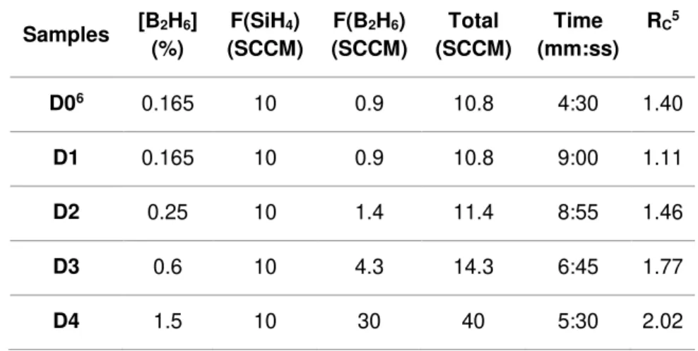
The processes described in the sections 2.1 to 2.5 were applied in this set of samples (See Appendix H). For this study were fabricated five sets of two samples (D[0-4] – A and B4). Each set have two shards (D[0-4] – A1 and B1), one for each diffusion profile. An alkali free glass substrate, AF45, was also used in order to measure further some electrical characteristics of the a-Si:H film. The masks used in the photolithographic process can be seen in Appendix I.
12 The goal was to produce p+n junctions with different B2H6/SiH4 flow rates. In Table 2.5 is visible the variations that were done for each set. The diffusion profiles used are both described on Table 2.2. To obtain an equivalent oxide thickness in the deep junction profile, the oxide growth process only occurred in the last 12 minutes of the diffusion. Aluminum planar and transversal contacts to substrate were made, followed by the annealing process.
For a more complete study, a thin film of indium oxide was deposited over the boron diffused region in order to improve the current-voltage characteristics under illumination.
Table 2.5 –Execution parameters with an rf potency of 5 W and a temperature setpoint of 90ºC.
Samples [B2H6] (%)
F(SiH4) (SCCM)
F(B2H6) (SCCM)
Total (SCCM)
Time (mm:ss)
RC5
D06 0.165 10 0.9 10.8 4:30 1.40 D1 0.165 10 0.9 10.8 9:00 1.11 D2 0.25 10 1.4 11.4 8:55 1.46 D3 0.6 10 4.3 14.3 6:45 1.77
D4 1.5 10 30 40 5:30 2.02
2.6.3. Oxide study
For this study were produced 16 samples – 2 sets of 8 samples each. To see the effect of different dopant doses in the oxide growth, half of them were doped7 with the conditions of D1 and the rest with the conditions of D4 (Table 2.5). The conditions used are described in Table 2.6.
Table 2.6 –Summary of the oxidation study.
Note: NA = Not Applicable
The aluminum contact definition was made resorting to DioCont mask (Appendix I) and to TI 35E photoresist. As said before, an increased speed was used in the spinner – 4000 rpm – for a longer period of time – 40 seconds. After the softbake, a low dose exposure –1 minute – was made. This allowed the patterning of all the five contacts. The substrates were kept at room temperature for 20 minutes. This delay time assures that the nitrogen generated during the exposure will diffuse
5 Growth rate.
6 The deposition conditions were based on D1, reducing the plasma reaction time, to obtain a thinner film.
7 The doping occurred only in half of the substrate as shown in the schematic. 8 O1-O8 is referred to [B2H6] = 1.5% and Ox1-Ox8 to [B2H6] = 0.165%.
Samples8 Temperature [C] Time [min] F(O2) [lpm] F(O2 bubbler) [lpm] F(N2) [lpm]
W et O xid atio n O1/Ox1 900 60
NA 0.8 1
O2/Ox2 50
O3/Ox3 40
O4/Ox4 30
Dry O xid atio n O5/Ox5 1000 60
0.8 NA 1
O6/Ox6 50
O7/Ox7 40
13 out of the resist. After this delay, the substrates were putted on the hot plate at 115ºC for 2 minutes in a process called ‘reversal bake’. The substrates were once again exposed, without a mask, for the flood exposure process. The dose, in this case, is very uncritical – at least 7 minutes of exposure. The photoresist developing was done using NaOH (6g/L) followed by the hardbake process, to ensure a good adhesion between the aluminum and the substrate. The aluminum etching was done using a home-made solution (HNO3:H3PO4:H2O – 6%:65%:29%). A scheme of the sample can be seen in Appendix J.
2.6.4. MOSFET fabrication
The MOSFET fabrication was based on the results of the previous studies. The sample preparation and lithographic process was the same of the other studies.
Each set contained two twin samples and a shard for process monitoring. In Appendix K are represented the masks used in the lithographic process. In this procedure, the gate oxide was not grown simultaneously to first diffusion. The recrystallized film was firstly removed, so that the gate oxide could be grown in the monocrystalline silicon surface. The bulk contact was made at the back of the substrate (aluminum transversal contact). The structure of the MOSFET (top view) as well as the channel dimensions are represented in Appendix L [52].
Several parameters were tested, such as, the dopant concentration (D1 and D4 conditions presented in Table 2.5), the diffusion profile (Table 2.2), the dielectric thickness (Table 2.6) and the oxide growth method – dry, wet and a combination of both – mix oxide. In the latter, the dry oxide thickness is only a small percentage of the total thickness (~100 Å) in order to improve the SiO2/Si interface. The temperature used in all wet oxide processes was 900ºC, whereas for the dry ones, an increase in the process temperature (1000ºC) was necessary.
2.7.
Electrical Characterization
Throughout the manufacturing, process control is essential to ensure that no problems occurred. A Veeco Dektak profilometer was used to measure the thickness of both materials, a-Si:H and silicon oxide. An abrupt step is necessary for a more accurate measure. The a-Si:H film thickness was measured on a sample deposited on a bare substrate glass, with a small region protected with a photoresist drop, for afterwards lift-off. Regarding the oxide, a selective etching (using HF solution) was made, plus a comparison between the color chart and the oxide thickness measured. The aluminum thickness was estimated using the BOC Edwards FTM7 Film Thickness Monitor (approximately 1500 Å).
Sheet resistance measurements were made using four-point-probe (FPP) technique (Veeco Instruments). It was used to measure sheet resistance of the shards, included in all the studies (except in the oxide one), and the indium oxide thin film deposited over glass. The latter was used to control the film properties deposited over the pn junctions.
For the current-voltage characteristics were used three different equipment: i) Keithley 228A, which served as a general voltage source; ii) Keithley 617, which was employed either as a source for gate voltage, as a low current ammeter (less than 20 mA) and as a voltmeter for direct measurements of the sample voltage in the case of high current measurements; iii) Keithley 195A used as ammeter when higher current values were measured. All the I-V measurements were done in a Faraday cage and under primary vacuum (9 × 10⁻¹ mbar).
14 to the sample (100V) and to measure its current, either in dark conditions during the σ(T) measurements, or under illumination, in the end, at room temperature, using a special halogen Philips lamp (ref. 13177) which reproduces fairly well the solar spectrum for AM1.5-AM2 [53]. Static electrical characterization was conducted at room temperature using the devices previous mentioned. The metal-semiconductor contacts and the pn junctions were tested obtaining the
I- V characteristics for each set of samples. In the junctions’ tests, it was obtained two groups of curves, one in the dark and the other under illumination of a Philips 13177 halogen lamp. The first was tested using a range [-5;1] V, swept with 0.4V step and with a 5 seconds stabilization time. The latter was similar, changing only the voltage range to [-1;1] V. On Appendix M it’s possible to see the electrical configuration used. The K228A was the voltage source and K617 measured the real voltage across the junction. The K195A was used to measure the current.
The oxide samples were subjected to both static and dynamic electrical characterizations. Firstly, it was made the static test to ensure the presence of good quality oxide. Each sample have four contacts, as represented in the Appendix J, tested from [-5;5] V with stabilization time of 30 seconds due to the low current values. The sample capacitance was also measured for each contact using a portable multimeter. For the dynamic characterization (C-V characteristics) it was used a 5208 Two Phase Lock-in Analyzer (EG&G PARC), a 4431 20MHz Programmable Function Generator (Schlumberger), a Current Sensitive Preamplifier – Model 181 (EG&G PARC) and a TDS 210 Two Channel Digital Real-Time Oscilloscope (Tektronix). The MOS-C structure takes time to become fully charged after a voltage step is applied, so C-V measurements can only be recorder after the device is fully charged, called the equilibrium condition (See Appendix N). To reach this condition a sufficient hold time is needed. This was guaranteed by the Lock-in readings of θ angle. The variation should be less than 1% relatively to the last value measured. In order to obtain a more precise measurement, the auto-range function of the Lock-in was activated and a 3 seconds time constant was used. Also, a pre-amplification of the signal was used (1 × 10⁻⁴). Two sweeps, commuted between -5 and 5 V (accumulation to inversion), were done, one at high-frequency (19990 Hz) and the other at low-high-frequency (990 Hz). In order to see trapped charges, a hysteresis curve was done for each functional contact. Both input and output signals were observed using the oscilloscope.
The MOSFET characterization consisted of five different tests of the device. Firstly, both junctions, bulk-drain (BD) and bulk-source (BS), were tested in the low current configuration, connecting K228A to the drain (or source) and the K617 to the bulk and measuring the current. A DC sweep was applied, ranging from -6 to 1 V9 with 1 second for stabilization time. The conductance and transconductance curve were obtained using the experimental assembly shown schematically in Appendix O. To obtain the transconductance curve the VDS was held constant at -6 V and a VGS sweep [0, -6]10 V was made, with a 0.2 V step, 5 seconds of stabilization time and 1 second of delay time. The conductance curve was obtained by sweeping both VGS and VDS, in the same interval as the transconductance curve. Also, the stabilization and delay time were the same. The gate of the MOSFET was electrically characterized, reading the current at the bulk terminal, connecting all the other terminals to the ground. In addition, a dynamic test was made (C-V curves), connecting the MOSFET as a MOS-C (short-circuit source and drain terminals), using the same assembly as explained above. Finally, an inverter circuit (See Appendix P) was done using a load resistor connected in series to the source terminal. The gate was connected to the function generator where a low frequency square signal of [0,-6] V was applied. The inverter was powered using the K228A voltage source.
9 The value of the positive voltage varied accordingly to the current measured in the direct bias condition. The objective was to see the behavior in the reverse bias condition to obtain the best junction.
15
3.
Results and Discussion
3.1.
Electrical characterization of metal-semiconductor
contacts
Metal-semiconductor contacts are a very important component of any semiconductor device. Consequently, it was important to explore how to make functional contacts, in order to be applied in the future devices produced.
This subchapter is, therefore, dedicated to the electrical characterization of the two architectures described previously, on section 2.6.1. As shown in a previous work [21, 23], aluminum is a p- type dopant in silicon and doesn’t make a good contact to lightly doped n-type silicon. A large mismatch between the Fermi energy of the metal and of the semiconductor can result in a high- resistance rectifying contact. For that reason, it was made a study on the structure of the contacts to obtain an ohmic behavior.
An ohmic contact is defined by the fact that it obeys to Ohm’s law, thus fulfilling the following two requirements: i) the threshold voltage for zero current is negligible with respect to the applied voltage; ii) the proportionality factor between current and voltage (i.e., conductivity) does not vary measurably with voltage. Both i) and ii) must be valid in a range, from about 1 mV to several Volts. Neglecting space-charge effects in the bulk, an ohmic contact will be present if the voltage drop at the electrodes is small compared with the total voltage drop across the semiconductor [54]. Therefore, if the work function of the metal is equal or smaller than the work function of the n-type semiconductor, an ohmic contact is present. In other words, it’s pretended that the Schottky barrier height, ϕB, is zero or negative. A simple scheme showing the work function and the Fermi level, regarding the metal-semiconductor interface, is presented in Appendix Q. As seen in the appendix, an accumulation-type contact is the preferred ohmic contact because electrons in the metal encounter the least barrier to their flow into or out the semiconductor.
According to the Schottky theory, the barrier height depends only on the metal work function and on the semiconductor electron affinity and is independent of the semiconductor doping density. As a result, one way to vary the barrier height is by using metals of the appropriate work function [17, 55]. Despite this, in the semiconductor industry, the materials used to form contacts are metals and silicides that are stable and relatively easy to process, so, it’s difficult to alter the barrier height by using metals of varying work functions. Also, it’s experimentally observed that the barrier height for the common semiconductors (Ge, Si and GaAs) and other III-V compounds is relatively independent of the work function of the metal. The situation described is sometimes attributed to Fermi level pinning [55]. The mechanisms that cause the Fermi level pinning is still
the subject of some disagreement, nevertheless, barrier height engineering is impractical. However, the barrier width can be easily changed varying the semiconductor doping density. Adding impurities will cause regions of high recombination rates. Also, heavily doped semiconductors have narrow space-charge region width (W~ND-1/2), allowing the electron tunneling effect [54, 55]. In order to create very thin space-charge region in the n-type silicon wafer, it’s required a minimum of phosphorus surface concentration (Cs) of 2 × 10²⁰ aṫ cm-3, as stated in the introduction chapter of this work.
To obtain the data needed to better evaluate the contact, the FPP was used for measuring the resistance and sheet resistance of the samples produced. Also, both resistance and sheet resistance values were obtained for the unprocessed 2’’ n-type silicon wafer in order to calculate the background phosphorus concentration (Nbc).
16 relation is possible since sheet resistance, and therefore resistivity, is uniquely related to the surface concentration of the diffused layer and, also, to the background concentration of the wafer. Regarding the C2 set of samples, they presented a considerably smaller sheet resistance, as expected, since these samples were submitted to the diffusion of phosphorus impurities from the a- Si:H (n+). This result implies that some of the dopant transferred become active in the silicon net. Consequently, this set presented satisfying properties, with sheet resistance of 22.9 Ω/□11. In order to know the n+-layer depth (x) and the surface concentration, we must take into consideration that upon such high concentrations in-diffusion of phosphorus, the kink-and-tail profiles can be described to occur due to dual diffusion mechanism, involving point defects of different origins and charge states [56]. As shown in these previous works [11, 57] done at LMSCE, it was obtained the phosphorus concentration in both the a- Si:H film, as deposited, and after the dopant diffusion, using the SIMS technique. It was determined that, for [PH3] = 1.5%, the dopant concentration was 1.3 × 10²¹ aṫ cm-3 and that it remains constant throughout the a- Si:H film thickness. So, the initial dose (QA0) present in the C2 set was 8.5 × 1015 cm-2 (obtained by multiplying the bulk a-Si:H initial concentration for the a-Si film thickness used in the set, 650 Å). It was shown that the a-Si concentration, after the diffusion at 1000ºC, is below the solid solubility, 9.3 × 10²⁰ aṫ cm-3 [57]. Since the dopant source is not unlimited, the best Fick’s law solution is fixed dose (QA) deposit, which represents a Gaussian profile:
2
( , )
exp
4
AQ
x
C x t
Dt
Dt
(3.1)Also, in the work previously mentioned, it was studied that equation 3.1 has a better correlation than when applying the erfc-type function. In light of the above, we obtain for the C2 set, the
following parameters: QA = 2.6 × 1015 cm-212; Cs = 5.2 × 10¹⁹ aṫ cm-3; and x = 1.7 µm (using the fitting parameter D = 1.3 × 10⁻¹¹ cm-2/min[57]). According to these results, the Cs obtained is lower than the minimum required in the literature, however since it is still a high surface concentration it is expected that this method still works in order to obtain ohmic contacts. Table 3.1 presents the results from the electrical characterization, made by the FPP, and the data obtained from equation 3.1:
Table 3.1 –Electrical and process parameters obtained for the C2 set.
Shard t (a-Si:H) [Å] tdiff/Ox [min] Tdiff/Ox [ºC] RS back [Ω/□]
<Cs> [aṫ cm-3]
<layer depth>
[μm]
tAl [Å]
C2-C 65
± 8×101 (B)
60± 1×101 (F) 60 1000 22.9 5.2×10
19 1.7 1630 (B) 1400 (F)
Note: (B) and (F) means back and front, respectively.
To investigate the influence of this highly doped layer (n+), we proceeded to the analysis of the I- V characteristics, obtained from both C1 and C2 sets. Each sample has four individual contacts, patterned in both sides of the sample. To better compare the results obtained, the square metal contacts and the diffusion area, being the latter only present on the C2 samples, were all similar and had a contact area of about 4 × 10⁻² cm2 and 9 × 10⁻² cm2, respectively. Also, regarding the samples’ structure and according to the direction of current flow, these contacts are considered
11 This value was obtained based on the equation R.3, with
V
I
=6.8 Ω and k=0.742.17 to be the vertical type, once the current is expected to flow mainly vertically in a rather uniform distribution [58].
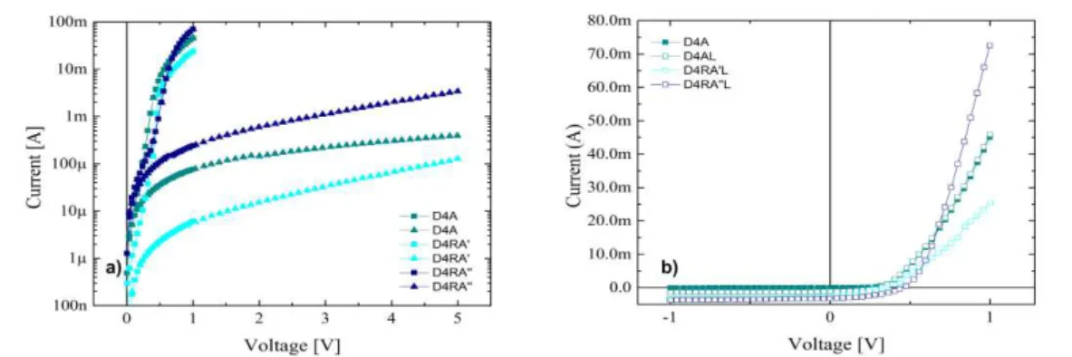
In Figure 3.1 are depicted the two sets of samples (C1 and C2).
Figure 3.1 –I-V characteristic curves, without heat treatment, of the a) C1 set, where the aluminum contacts
were directly deposited over the sample’s surface, and b) C2 set, which received a highly doped n-type a-Si:H film for dopant diffusion.
In Figure 3.1 a) eight I-V curves are presented for each contact in the C1 set. The applied voltage was similar for almost every contact, except when the current limit, supported by the ammeter, was reached. As stated early on this chapter, it was expected that this metal- semiconductor junction would create a Schottky barrier, resulting in low forward voltage drop. In fact, that happen for almost every contact tested, forming a typical Schottky diode. In this case, for lightly-doped semiconductors (≤3×10¹⁷ aṫ cm-3 [17]), the current flows as a result of thermionic emission (TE), with electrons thermally excited over the barrier [33] (see Appendix S). As experimentally observed by Werner [59], the I-V curves show to be composed of two or more components of current. The linear portion of the I-V curve is usually attributed to the main conduction mechanism, namely TE, and the leakage current is due to generation and recombination in the space charge region and edge-related conduction. However, in this lot, we can observe a significantly different behavior from the C1A-1, C1A-4 and C1B-1 contacts when compared with other. In special, the last two contacts mentioned present a quasi- ohmic behavior. This can be justified by a possible
spatial variation of the Schottky barrier height at the metal-semiconductor interface. This barrier height variation is commonly associated with electronic states due to defects and metal-induced gap states. However, the relationship between the Schottky barrier height and the interface structure has not been assessed thoroughly [60]. Though, it is suggested that the majority of metal- semiconductor interfaces have inhomogeneous Schottky barrier heights and, consequently, the Fermi level position at the interface is not pinned, being determined by local parameters which vary spatially at the interface. As a result, the inhomogeneity in the Schottky barrier have a dominant effect on electron transport. Furthermore, the behavior of C1A-4 and C1B-1 may also be due to some impurities on the interface, enabling a higher forward current. The Figure 3.1 b) shows the C2 set before the heat treatment process. We can observe several differences between the two sets, however a quite big dispersion in the results is also present in this one, in special in the C2A’s contacts. Once the C2A and C2B are twin samples, this dispersion may be associated with intrinsic factors of the manufacturing process. When comparing the a) and b) plots, it is clear that the C2 contacts are clearly better than the C1 ones, reaching higher current values for the same applied voltage. The n+- layer plays an important role, once for high doping densities (≥2×10²⁰ aṫ cm-3 [17]) the barrier is sufficiently narrow at or near the bottom of the conduction band for the electrons to tunnel directly, in an effect called field emission (FE) [61]. However, it’s clear that these are not ohmic contacts, once they not fulfill the requirements stated
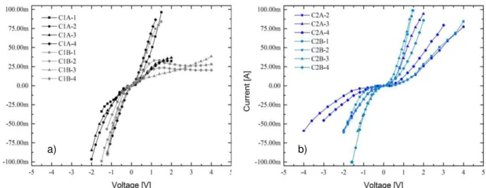


![Table 3.2 – Surface concentration, junction depth and electrical parameters for the 5 sets of samples produced, D [0-4], regarding the a-Si:H (p + ) film](https://thumb-eu.123doks.com/thumbv2/123dok_br/16693494.743728/40.892.81.815.567.1029/surface-concentration-junction-electrical-parameters-samples-produced-regarding.webp)