Ângelo Emanuel Neves dos Santos
Licenciado em Ciências da Engenharia de Micro e Nanotecnologias
Design and simulation of a smart bottle with
fill-level sensing based on oxide TFT technology
Dissertação para obtenção do Grau de Mestre em
Engenharia de Micro e Nanotecnologias
Orientador:
Doutor Pedro Miguel Cândido Barquinha,
Professor Auxiliar, Faculdade de Ciências e Tecnologia,
Universidade Nova de Lisboa
Co-orientador:
Doutor João Carlos da Palma Goes,
Professor Associado com Agregação, Faculdade de
Ciências e Tecnologia, Universidade Nova de Lisboa
Presidente: Professor Doutor Rodrigo Ferrão de Paiva Martins Arguente: Professor Doutor Vítor Manuel Grade Tavares
Vogal: Professor Doutor Pedro Miguel Cândido Barquinha
i
Design and simulation of a smart bottle with fill-level sensing
based on oxide TFT technology
Copyright © Ângelo Emanuel Neves dos Santos, Faculdade de Ciências
e Tecnologia, Universidade Nova de Lisboa.
iii
“
The beginning of wisdom is found in doubting; by doubting we come to the
question, and by seeking we may come upon the truth.
”
v
Acknowledgments
A finalização desta dissertação representa uma enorme etapa na minha vida, sendo que durante estes cinco anos de estudo na Faculdade de Ciências e Tecnologias tenho a agradecer a muitas pessoas, muitos momentos, e muitos problemas que fizeram de mim o que eu sou hoje.
Em primeiro lugar, não poderia deixar de agradecer ao Prof. Dr. Rodrigo Martins e à Prof.ª Dra. Elvira Fortunato, pela criação do magnífico mestrado em Engenharia de micro e nanotecno-logias, cuja excelência e multidisciplinaridade é verdadeiramente notável para qualquer um que entenda a natureza dos conceitos científicos que são lecionados. Complementando o curso, os professores criaram ainda as excelentes instituições CENIMAT|i3N e CEMOP providenciando os meios científicos e tecnológicos necessários para o avanço da investigação nos mais diversos ramos nas áreas de materiais e da eletrónica, tendo eu a agradecer a possibilidade de trabalhar e de fazer parte de um grupo com uma qualidade e renome de nível mundial.
Em segundo lugar gostaria de agradecer aos meus orientadores Prof. Pedro Barquinha e Prof. João Goes sendo que ambos foram importantíssimos no desenvolvimento deste projeto. Ao Prof. Pedro tenho a agradecer toda a motivação e votos de confiança que me foram dados ao longo do projeto, e ainda por toda a ajuda e conhecimentos partilhados para que os objetivos finais fossem atingidos. Ao Prof. João Goes tenho a agradecer toda a ajuda inicial no desenvol-vimento e consolidação dos requisitos necessários do projeto a nível eletrónico, sendo esta ful-cral para o correto desenvolvimento do mesmo. Não podendo deixar de agradecer pela disponi-bilidade de ambos os professores, que apesar do pouquíssimo tempo livre, sempre se mostraram disponíveis para que eu, em caso de qualquer dúvida, não hesitasse em contactar.
Gostava ainda de deixar o meu agradecimento ao Prof. João Pedro Oliveira, foi graças a ele e às suas motivadoras aulas e palestras que descobri a minha paixão pelo mundo da eletró-nica, muito obrigado por todas as conversas fora de aula sobre os mais diversos temas.
Gostaria também de deixar o meu enorme agradecimento à Ganga Bahubalindruni, que se mostrou incansável no apoio em tudo o que pudesse estar relacionado com o projeto. Obrig-ado pela ajuda no debugging de vários blocos eletrónicos e ainda pelos conhecimentos trans-mitidos relativamente ao desenho de layouts.
Um especial obrigado aos meus grandes amigos e colegas “Mágico” e José Rosa.
Nada disto seria possível sem o apoio da minha família, a eles devo tudo o que tenho hoje, um muito obrigado a todos, nomeadamente às minhas irmãs Sandrina, Cindy e Priscilla pela motivação, alegria e maluquice que me transmitem todos os dias, ao meu Pai Manuel, à minha segunda família da qual fazem parte a Maria e o Diogo pelo carinho e apoio que me dão desde que era praticamente uma criança, e especialmente à minha mãe, por todos os conselhos, e por toda a ajuda ao longo dos meus anos de vida. Mãe, não existem palavras que possam descrever a minha gratidão por tudo o que fizeste por mim, sei que, contigo posso contar até ao final da vida!
Um infinito obrigado à minha namorada Rutie, por tudo e por nada. Por tudo o que fazes por mim para me ver feliz e por nada mudar ao longo de todos estes anos. És, e sempre serás das pessoas mais importantes da minha vida, e a ti agradeço-te tudo. Mesmo sem perceberes a área cientifica em que trabalho, consegues-me sempre ajudar com as tuas palavras e ideias malucas, nunca mudes.
Obrigado ainda ao meu “tropa” Mihai Cotoman, por todos aqueles momentos que só ele sabe, e por todas as conversas “cientificas” e cafés que ajudaram a desanuviar a cabeça de
todos os problemas que surgiam.
Em último lugar não posso deixar de agradecer a todos os amigos exteriores à faculdade que de alguma forma me ajudaram ao longo da minha vida: Ivan Côrte-Real, João Miguel, André Pinto, Fernando Vieira, Diogo Araújo, Natacha Moreira, Diogo Fernandes, Filipe Macário, e todos os restantes que me possa ter esquecido.
vii
Abstract
Packaging is an important element responsible for brand growth and one of the main rea-sons for producers to gain competitive advantages through technological innovation. In this re-gard, the aim of this work is to design a fully autonomous electronic system for a smart bottle packaging, being integrated in a European project named ROLL-OUT. The desired application for the smart bottle is to act as a fill-level sensor system in order to determine the liquid content level that exists inside an opaque bottle, so the consumer can exactly know the remaining quantity of the product inside.
An in-house amorphous indium–gallium–zinc oxide thin-film transistor (a-IGZO TFT)
model, previously developed, was used for circuit designing purposes. This model was based in an artificial neural network (ANN) equivalent circuit approach.
Taking into account that only n-type oxide TFTs were used, plenty of electronic building-blocks have been designed: clock generator, non-overlapping phase generator, a capacitance-to-voltage converter and a comparator. As it was demonstrated by electrical simulations, it has been achieved good functionality for each block, having a final system with a power dissipation of 2.3 mW (VDD=10 V) not considering the clock generator. Four printed circuit boards (PCBs)
have been also designed in order to help in the testing phase.
Mask layouts were already designed and are currently in fabrication, foreseeing a suc-cessful circuit fabrication, and a major step towards the design and integration of complex trans-ducer systems using oxide TFTs technology.
Keywords: Smart packaging; a-IGZO TFTs; capacitance-to-voltage converter;
ix
Resumo
As embalagens são um elemento importante no crescimento de determinadas marcas e uma das principais razões pelas quais certos produtores ganham vantagem competitiva através de inovações tecnológicas. Neste âmbito, o objetivo deste trabalho corresponde ao desenvolvi-mento de um sistema eletrónico totalmente autónomo para uma garrafa inteligente, estando este integrado num projeto europeu designado de ROLL-OUT. A aplicação pretendida da garrafa, é que esta contenha um sistema sensível ao nível de enchimento do liquido da mesma, de forma a que o consumidor possa determinar, de forma exata, a quantidade restante de produto ex-istente dentro de uma garrafa opaca.
Para o propósito de desenho de circuitos, foi usando um modelo de transístores de filme fino baseados em óxido de gálio-índio-zinco amorfo (a-IGZO TFTs), sendo que o mesmo fora anteriormente desenvolvido. Este modelo foi baseado numa aproximação de circuitos equiva-lentes através de redes neuronais artificiais.
Tendo em conta que apenas transístores do tipo-n foram utilizados, foram desenvolvidos vários blocos eletrónicos: gerador de relógio, gerador de fases não sobrepostas, conversor ca-pacidade/tensão e um comparador. Tal como foi demonstrado através de simulações elétricas, foi alcançada uma boa funcionalidade para cada bloco, tendo-se obtido um sistema final com uma dissipação de potência de 2.3 mW (VDD=10 V), não considerando o gerador de relógio. Foram ainda desenvolvidas quatro placas de circuito impresso com o objetivo de futuramente auxiliar o teste dos circuitos produzidos.
Os layouts das máscaras já foram desenvolvidos estando neste momento em fase de fab-ricação, prevendo-se assim uma produção de circuitos bem-sucedida, e um grande passo no desenvolvimento e integração de sistemas transdutores complexos usando a tecnologia de transístores de óxidos semicondutores.
Palavras-chave: Embalagens inteligentes; a-IGZO TFTs; conversor
xi
Contents
Acknowledgments ... v
Abstract ... vii
Resumo ... ix
Contents ... xi
List of figures ... xiii
List of Tables ... xv
Symbols ... xvii
Acronyms ... xix
1
Motivation and Objectives ... 1
2
Introduction ... 3
2.1 Thin-Film Transistors ... 3
2.2 Capacitance-to-voltage converters ... 7
2.3 Comparators ... 8
3
Materials and Methods ... 9
3.1 Modelling, Design and Simulation Tools ... 9
3.2 Electrical characterization of transistors and circuits... 10
4
Results and Discussion ... 11
4.1 Fill level sensing in smart bottle: Concept and Block Diagram ... 11
4.2 Circuit design, simulations and layouts ... 12
4.3 Printed circuit board design ... 33
5
Conclusions and Future Perspectives ... 35
6
References ... 37
7
Annexes ... 39
Annex A – Design rules considered in each layer ... 39
Annex B – Transistor dimensions ... 41
xiii
List of figures
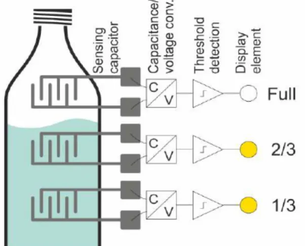
Figure 1.1- Scheme of the smart bottle functioning principle and the main electronic blocks. ... 1
Figure 2.1- Scheme of the most conventional TFT strutures, according to the position of the gate electrode and sorce/drain electrodes relatively to the semiconductor, adapted from [1]. ... 4
Figure 2.2- Ideal output curves of a n-type TFT, adapted from [37]. ... 5
Figure 2.3- Voltage transfer characteristic of a comparator with infinite gain, adapted from [27]. 8 Figure 4.1- Block diagram of the full fill-level sensing smart bottle system... 11
Figure 4.2- Staggered bottom gate structure of the IGZO TFTs, adapted from [30]. ... 13
Figure 4.3- Verilog-A neural model performance validation from the measurements 0 ≤ VDS ≤ 10 V in steps of 0.5 V and 2 ≤ VGS ≤ 6 V in steps of 2 V.(a)- Output characteristics curvers of the TFT. (b)- C-V characteristics curves CGSi. (c)- CGDi. Adapted from [29]. ... 13
Figure 4.4- (a)- Circuit schematic of an inverter with a diode-connected load. (b)- Transient simulation result for the inverter considering the n-type load W/L= 10/20 µm/µm and driver W/L= 80/20 µm/µm. ... 14
Figure 4.5- Layout of the inverter circuit. ... 15
Figure 4.6- (a)- Circuit schematic of a NAND with a diode-connected load. (b)- Transient simulation result of the NAND considering the n-type load W/L= 10/20 µm/µm and drivers W/L= 80/20 µm/µm. ... 16
Figure 4.7- Layout of the NAND gate circuit. ... 16
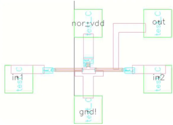
Figure 4.8- Circuit schematic of a NOR with a diode-connected load. (b)- Transient simulation result of the NOR considering the n-type load W/L= 10/20 µm/µm and drivers W/L= 80/20 µm/µm. ... 17
Figure 4.9- Layout of the NOR gate circuit. ... 18
Figure 4.10- Scheme of a 23-stages ring oscillator... 19
Figure 4.11- 23-stages ring oscillator layout ... 19
Figure 4.12- (a)- Circuit schematic of a D-type flip-flop. (b)- Scheme of the frequency divider feedback connections using a D-type flip-flop. ... 20
Figure 4.13- D-type flip-flop counter layout ... 20
Figure 4.14- Scheme of the clock generator, comprising the ring oscillator and the 4-bit counter. ... 21
Figure 4.15- Simulation result of the 4-bit counter, when the signal generated by the ring oscillator is given as an input. ... 21
Figure 4.16- Circuit schematic of the non-overlapping phase generator. ... 22
Figure 4.17- Layout of the phase generator. ... 22
Figure 4.18- Simulation result of the non-overlapping phase generator when the clock signal is given as an input. ... 23
Figure 4.20- (a)- Transient simulation result of the C/V converter when there is no water in the capacitive sensor (5 pF). (b)- Transient simulation result of the C/V converter when there is water in the capacitive sensor (10 pF). ... 25 Figure 4.21- Layout of the C/V converter. ... 25 Figure 4.22- (a)- Circuit schematic of the latch. (b)- Circuit schematic of the doble to
single-ended converter. ... 26 Figure 4.23- Layout of the latch and the doble-to-single ended converter ... 27 Figure 4.24- (a)- Circuit schematic of a regular common source amplifier having a positive
feedback unit. (b)- Circuit schematic of the differential amplifier where the feedback network can be observed, adapted from [31]. ... 27 Figure 4.25- (a)- Bode magnitude plot of the differential amplifier. (b)- Simulation result of the
differential amplifier output response with a differential triangular signal with 0.22V
amplitude as input. ... 28 Figure 4.26- Layout of the positive-feedback amplifier. ... 29 Figure 4.27- (a)- Simulation result of the comparator output when a differential voltage sweep is
applied. (b)- Simulation result of the comparator output when a input triangular signal is applied. ... 30 Figure 4.28- Circuit schematic of the low pass filter... 31 Figure 4.29- Bode magnitude plot of the low-pass filter. ... 31 Figure 4.30- (a)- Result simulation of the final system output when there is not water in the
capacitive sensor. (b)- Result simulation of the final system output when there is water in the capacitive sensor. ... 32 Figure 7.1- PCB schematic (a) and layout (b) for testing the capacitance-to-voltage converter. 43 Figure 7.2- PCB schematic (a) and layout (b) for testing the positive feedback differential
xv
List of Tables
Table 2.1- Comparison between some of the main characteristics for the different types of TFTs technologies based on [14], [16]–[18]. ... 6
Table 4.1- Representation of both capacitors charge in phase one and two. ... 24
xvii
Symbols
Cox - Gate oxide capacitance per unit area
Gm– Transconductance of a transistor
IDS– Current between drain and source
IGS– Current between gate and source
L – Channel length
Q – Capacitor charge
r0 – Output resistance of a transistor
VDS– Voltage between drain and source
VGS– Voltage between gate and source
VIH– Input high voltage
VIL– Input low voltage
VOH– Output high voltage
VOL– Output low voltage
VON– Turn-on voltage
VOS – Voltage offset
VT – Threshold voltage
W – Channel width
µFE – Field-effect mobility
µSAT – Saturation mobility
λ – Channel-length modulation parameter
xix
Acronyms
a-IGZO – Amorphous indium-gallium-zinc oxide
a-Si– Amorphous silicon
a-ZTO – Amorphous zinc-tin oxide
ANN – Artificial Neural Network
CEMOP – Center of Excellence in Microelectronics Optoelectronics and Processes
CMOS – Complementary metal-oxide-semiconductor
CVD – Chemical vapor deposition
C/V – Capacitance-to-voltage
DRC – Design rule check
EC – Equivalent circuit
FET – Field-effect transistor
IT – Information technology
LCD – Liquid-crystal display
LTPS – Low temperature polycrystalline silicon
MOSFET – Metal-oxide-semiconductor field-effect transistor
OTFT – Organic thin-film transistor
PCB – Printed circuit board
PDK – Process design kit
Poly-Si – Polycrystalline silicon
RT – Room temperature
SMU – Source measure unit
TCO – Transparent conductive oxide
TFT -Thin-film transistor
TSO – Transparent semiconducting oxide
1
1
Motivation and Objectives
In the last years, the huge development of transparent conducting oxides (TCOs) and transparent semiconducting oxides (TSOs) have opened the door to a new era of transparent and flexible electronics based on oxide thin-film transistors (TFTs). This technology has been gaining a paramount importance in almost every field where it can be applied on, such as fully transparent displays, smart windows and watches or even wearable electronics [1]–[6]
The aim of this work is to design a fully autonomous electronic system for a smart bottle packaging and it is integrated in a European project named OUT. The goal of the ROLL-OUT project is to create a multi-purpose technology for, thin, large-area, high-performance, smart, and autonomous systems comprising integrated circuits, sensors, electronics, advancing pack-ages, automotive interiors and textile industries beyond their traditional scope.
The ROLL-OUT project is envisioned to have direct impact on manufacturing capability and value-addition of consumer goods in Europe. The project consortium partners are from various section of the large-area, flexible systems industry value chain being some of them: UNINOVA, VTT, IISB, CIDETEC, PICOSUN, LOGOPLASTE and POLYTEKNIK. The work presented in this doc-ument is thus part of UNINOVA’s contribution for the project, aiming the design and simulation of integrated circuits (where the main blocks can be identified in figure 1.1) based on models devel-oped for amorphous indium-gallium-zinc oxide (IGZO) TFTs produced at low temperature (180 °C) on flexible substrates. Other partners of the
project develop in lab scale the remaining com-ponents of the final smart bottle, namely capac-itive sensors and printed batteries, which are then trasfered to industrial partners for fabrica-tion in large scale roll-to-roll systems. All these components are developed according to the re-quirements of a bottle specifically designed for this project by the partner Logoplaste Innova-tion Lab.
Packaging is an important element re-sponsible for brand growth and the main reason for producers to gain competitive
ad-vantages through innovation, and is leading companies to look with ever-more interest for the integration of sen-sors capable of giving a clear feed-back on the shelf life of the products.
3
2
Introduction
In this chapter an introductory background will be summarized, giving special focus to the TFTs structure, operation principle, and also their technological evolutions. It will be also briefly explained the functionality and typical structure of the main electronic blocks used in the smart bottle system, namely the capacitance-to-voltage converter and the comparator.
2.1 Thin-Film Transistors
In a world of constant technology evolution, there are always common goals in almost every scientific field, like reducing costs, achieving better performance, having less power con-sumption and creating technological innovations.
Nowadays one of the major researching themes is transparent and flexible electronics, in which TFTs acquire an important role due to their advantages over the existing transistors tech-nology, which will be presented further.
2.1.1 TFTs structures and operation principle
A TFT is basically a field-effect transistor (FET) composed, by three terminals named gate, source and drain, a semiconductor and a dielectric layer, just like a standard metal-oxide-semiconductor field-effect transistor (MOSFET). The metal-oxide-semiconductor is located between the source and drain contacts and the dielectric is placed between the gate electrode and the semi-conductor layer.
TFTs are more focused on large area and low processing temperature electronics, while the regular MOSFET technology main prominence is to achieve high performance devices, alt-hough it needs high processing temperatures.
The working principle of a TFT consists in the modulation of the current that flows be-tween the drain and source contacts (IDS) by applying a potential between the gate and source
(VGS), therefore the modulation is achieved by a capacitive injection of carriers close to the
die-lectric/semiconductor interface [7].
TFTs can have several structures, the most common ones can be observed in figure 2.1. The structure’s name depends whether the source/drain and gate electrodes are on the same or opposite side of the semiconductor, being identified as coplanar or staggered structure respec-tively.
of liquid-crystal displays (LCDs), the staggered bottom-gate configuration is preferred since the typically used a-Si:H TFTs are light sensitive and this structure allows the shielding of the semi-conductor by the metal gate electrode. Conversely, in poly-Si TFTs, a coplanar top-gate structure (where the semiconductor is first deposited) is generally preferred, since the semiconductor crys-tallization process requires high temperatures that can damage and degrade other layers previ-ously deposited.
Figure 2.1- Scheme of the most conventional TFT strutures, according to the position of the gate electrode and sorce/drain electrodes relatively to the semiconductor, adapted from [7].
In terms of operating principle, considering an n-type TFT, the positive or negative value of the threshold voltage (VT) will dictate if the transistor is in enhancement or depletion mode
respectively. Generally the enhancement type transistors are preferred since no VGS is needed to
turn off the transistor, simplifying the circuit design and minimizing power dissipation [8].
When VGS≪VT the transistor dielectric/semiconductor interface is depleted of electrons
and negligible current flows, resulting in the Off-state.
When VGS>VT the dielectric layer acts like a capacitor, so that in the semiconductor
5
𝐼
𝐷𝑆= 𝜇
𝐹𝐸. 𝐶
𝑜𝑥×
𝑊
𝐿 (
(𝑉
𝐺𝑆− 𝑉
𝑇)𝑉
𝐷𝑆−
𝑉
𝐷𝑆 22 )
(1)Where 𝜇𝐹𝐸 is the field-effect mobility in cm2/(V.s), 𝐶
𝑜𝑥 is the oxide capacitance in F/cm2
and W and L are the TFT channel width and length.
On the other hand, if VDS>>VGS-VT the semiconductor close to the drain region becomes
depleted and a phenomenon designated by pich-off occurs leading to the saturation mode, where ideally IDS is independent of VDS and the current can be expressed by:
𝐼
𝐷𝑆=
𝜇
𝑠𝑎𝑡2
. 𝐶
𝑜𝑥×
𝑊
𝐿
(𝑉
𝐺𝑆− 𝑉
𝑇)
2(2)
Although, when the drain voltage becomes too high, or the channel length becomes too short, non-ideal effects can arise, such as IDS increase with VDS in saturation mode, a phenomena
called channel-length modulation [10]. To take this effect into account equation (2) can be modi-fied as follows, where λ is the channel-length modulation parameter:
𝐼
𝐷𝑆=
𝜇
𝑠𝑎𝑡2
. 𝐶
𝑜𝑥×
𝑊
𝐿
(𝑉
𝐺𝑆− 𝑉
𝑇)
2×(1 + 𝜆. 𝑉
𝐷𝑆)
(3)2.1.2 TFTs technology evolution
As mentioned above, TFTs are funda-mental building blocks for today’s breakthroughs in microelectronics, like plastic based flat-panel displays, wearable computers or even paper electronics [11]–[13]. So it is quite expected, and noticeable that the scientific research on this top-ics has greatly increased since these last few years [7].There are different technologies in which the TFTs are based on, for instance, organic thin-film transistors (OTFTs) have been intensively researched, because of their properties allowing to reduce the processing temperature and cost when compared to a-Si TFTs, giving also the possibility to perform roll-to-roll manufacturing [14]. Nonetheless, the relatively low mobility and
poor bias stability of a-Si and organic TFTs may limit their practical usage in some applications. In low-temperature poly-Si (LTPS) it is possible to achieve values of mobility up to 100 cm2/V.s
and excellent device stability, but it requires a high temperature processing as well as an expen-sive crystallization and doping process, which prevent the use of plastic substrates [15].
In this regard, metal oxide TFT technology has recently gained considerable importance, due to its high mobility, low temperature processing, good transparency to visible light, low power consumption, faster response times and relatively low fabrication cost [7].
Therefore, oxide TFTs potentiate a significant cost reduction from poly-Si TFTs, since these can be fabricated without needing a crystallization or doping process. It can be observed in table 2.1 a brief review of the TFT main parameters for the technologies aforementioned.
Table 2.1- Comparison between some of the main characteristics for the different types of TFTs technol-ogies based on [14], [16]–[18]
Considering all the oxide TFT technology features mentioned, it is understandable why this technology created such a big research interest all over the world. The mainstream and most optimized oxide TFTs are the ones based in amorphous indium-gallium-zinc oxide (a-IGZO). In fact, since the initial work on IGZO TFTs of Prof. Hosono’s group in Tokyo Institute of Technology
in 2004, many laboratories and industries around the world adopted this material for developing TFTs. In 2010, C. J. Chiu et al. produced an a-IGZO TFT using Ta2O5 as gate dielectric that had
a high field-effect mobility of 61.5 cm2/V.s, a subthreshold voltage swing of 0.61 V/decade and a
LTPS TFT
a-Si TFT
Organic TFT
Oxide TFT
Stability
High
Low
Low
High/medium
Mobility (cm
2/V.s)
< 100
< 1
< 10
10-60
Yield
Medium
High
High
High
Deposition Technique
CVD+Exci-mer Laser
PECVD
Printing or vacuum
evaporation
Sputtering or
printing
Processing Temperature
(°C)
< 500
250 - 350
RT
RT - 300
Substrate
Glass or
Metal
Glass,
Metal or
Plastic
Glass, Metal or
Plastic
Glass, Metal or
7
Another approach that has been considered to simplify and reduce processing costs is the fabrication of TFTs by printing the layers with a solution based precursor. The standard methods used for producing electronic devices are based on the sequential deposition, patterning and etching of different layers, involving mostly vacuum-based technologies, which contribute to a high manufacturing cost. Direct printing of inorganic materials allows to deposit films using a direct additive patterning process, enabling high-performance and low-cost electronics. The main issue in this kind of approach is the difficulty in preparing ink-jet-printable precursors conjugated with a desired performance, however in this process no masks or screens are needed and since it is an additive process, materials are applied only where desired. When using direct printing a cpst reduction of 64% is achieved when compared to the standard microelectronics technologies [7].
K.K. Banger et al. were able to fabricate a reproducible and high operationally stable IGZO solution-processed TFTs with field-effect mobilities of 10 cm2/V.s and a subthreshold slope of
0.42 V/decade, plus the devices fabrication was made with a maximum temperature of 230 °C allowing the future integration of this technology with flexible substrates [21].
There is also a lot of research in the development of p-type oxide TFTs since these have instability issues and are very limited by the low hole mobility. When high performance p-type TFTs are obtained a new era of oxide-based electronics certainly will arise, by allowing the pro-duction of complementary metal-oxide-semiconductors (CMOS) which is the core for the microe-lectronics of information technology (IT), permitting the use of compact and ultra-low power con-sumption circuitry [7].
All the referred topics lead to a huge capability of circuit integration using oxide TFTs tech-nology, in this regard the next subsections will briefly explain the functionality of the most im-portant electronics blocks used in the smart bottle system.
2.2 Capacitance-to-voltage converters
Capacitance is one of the most broadly used parameters in sensors applications, therefore many circuits have been developed to convert capacitance variations into measurable electric signals. This kind of circuitry is widely used in several scientific fields, for example, in the meas-urement of physical quantities such as density, force or even blood pressure and component concentration in multicomponent fluids [22]–[24]. This electronic circuit is denominated as a ca-pacitance-to-voltage (C/V) converter, and when attached to a capacitive sensor they form an electrically measurable capacitive transducer.
C/V converters can be based on direct or indirect conversion methods. In the direct method the capacitance is directly converted into voltage while in the indirect it first occurs a conversion into frequency or time and only then the conversion to voltage [25].
Since this project aims to use simple, high yield but still reliable and functional circuits it was adopted a direct type C/V converter based on a charge distribution method
It is important to emphasize that to the author’s knowledge there are no reports in literature regarding the use of oxide TFTs in designing any type of C/V converter.
2.3 Comparators
The comparator is one of the most important blocks since early electronic developments. The main function of this block is to compare two analog input voltage levels and produce an output digital signal that depends in the magnitude of both. A comparator is basically used when-ever a comparison of voltages or currents is needed, for example in zero-crossing detectors, relaxation oscillators, level shifters or analog-to-digital converters [26]–[28].
The following equation and voltage transfer curve represents the real functioning of a com-parator, i.e. without an infinite gain.
𝑉𝑜𝑢𝑡= {
𝑉𝑂𝐻 , 𝑖𝑓 (𝑉𝑖𝑛+− 𝑉𝑖𝑛−) > 𝑉𝐼𝐻 𝐴𝑣(𝑉𝑖𝑛+− 𝑉𝑖𝑛−), 𝑖𝑓 𝑉𝐼𝐿< (𝑉𝑖𝑛+− 𝑉𝑖𝑛−) < 𝑉𝐼𝐻
𝑉𝑂𝐿, 𝑖𝑓 (𝑉𝑖𝑛+− 𝑉𝑖𝑛−) < 𝑉𝐼𝐿
(4)
Figure 2.3- Voltage transfer characteristic of a comparator with infinite gain, adapted from [27].
9
3
Materials and Methods
3.1 Modelling, Design and Simulation Tools
This project was realized using an in-house TFT model that was performed using artificial neural network (ANN) based equivalent circuits (EC) to predict static and dynamic behavior of the devices. To build the model, measurements were previously done in order to extract the devices main parameters, then an EC is derived from the devices structure and each electrical element in it is modeled with an ANN. Lastly these networks are implemented in Verilog-A [29].
The main software used in this project was Cadence Design Systems, allowing to perform the schematics and layout design and the respective simulations, using VirtuosoTM Platform and
SpectreTM Simulator.
For the layouts design, it was used an in-house process design kit (PDK) based on the existing fabrication processes limitations and adapted to the optical lithography constrains avail-able at CEMOP/UNINOVA, considering a safety misalignment factor to prevent undesiravail-able ef-fects. Along other feautures, the PDK includes both design rule check (DRC) and layout versus schematic (LVS) verification decks.
The DRC determines if a layout satisfies a series of recommended parameters called de-sign rules, imposed by the fabrication processes. The rules used for each layer, during the circuit layout are presented in A annex.
LVS is a method of verifying that the layout of the design is functionally equivalent to the respective schematic, i.e. if they have the same electrical connections and therefore the sche-matic can be obtained from the layout.
3.2 Electrical characterization of transistors and circuits
Since the future step of this work is to test the whole involved devices and building blocks of the system, electrical characterization is of major importance. For this purpose, the transfer and output curves of the different sized TFTs will be performed in ambient conditions, inside a faraday cage, using an Agilent 4155C semiconductor parameter analyzer connected to a Cas-cade Microtech M150 manual microprobe station, controlled by the software Metrics ICS. The Agilent measurements can be performed with different ranges depending on the testing circuit.
11
4
Results and Discussion
This chapter discusses the results regarding the design and the electrical simulations of all the necessary building-blocks to implement the smart bottle system, being divided in three main sections; in the first one an overview of the system is given as well as an explanation of what ideally happens to the electrical signal in each block; in the second section the emphasis is given to the design and layout of the blocks described before, where simulation results using the IGZO TFT model are described; the last section is dedicated to the design of the schematics and layouts of the four testing PCBs.
4.1 Fill level sensing in smart bottle: Concept and Block
Diagram
It is important to refer that the final adopted system topology presented results from the discussion among the partners of the project, having the common objective of producing simple and cheap circuits. It was also imperative to keep the transistor count as low as possible in order to maximize yield during the future processing of the circuits in lab-scale.
In figure 4.1 it is presented the block diagram of the full smart bottle system. The system only needs a supply voltage in order to start operating. Firstly, a clock signal is generated by the 23-stage ring oscillator being then its frequency divided by a factor of 16 imposed by the D-type flip-flop 4-bit counters. These two blocks represent the clock generator. Then, the produced clock signal is applied to the input of the clock-phase generator that consequently generates two non-overlapping phases at the output. These two non-non-overlapping phases serve as inputs of the C/V converter whose output response will depend on the capacitive sensor value (more details in the following section).
In the comparator, first an amplification of the differential voltage between the two inputs occur. Then the latch gives an output of VDD or VSS depending on which input has a higher voltage
value. The reference voltage value of the comparator was chosen in order to be between the voltage values obtained at the output of the C/V converter in each scenario (either with or without liquid). Hence, when there is no liquid in the capacitive sensor, the output signal of the C/V con-verter is always lower than the reference voltage resulting in the low state of the comparator. On the other hand, when there is liquid in the sensor, a capacitance gain occurs in the sensor result-ing in a higher voltage and in the high state of the comparator.
After the comparator a switch fed by phase two is used in order to only sample the voltage comparison in this same phase, where the signal actually depends on the sensor capacitance unlike phase one (more details given in the next section).
In the last stage a low-pass filter is implemented in order to eliminate high frequency components that may arise and degrade the circuit performance. Finally, the signal reaches a display element which depending on the applied voltage can be either in on or off state, i.e. illu-minated or not.
The smart bottle has an active area of 1.8 x 10 cm2, in which three independent systems
will be implemented allowing the control of three different electrochromic cells, as presented in figure 1.1. Also, the whole system will operate at a frequency of few kHz.
All the above-mentioned functional blocks will be explained, in detail, in the next section.
4.2 Circuit design, simulations and layouts
As stated before, based on the aforementioned concept all the necessary building blocks were designed and simulated using Cadence Design Systems, being ordered in this section fol-lowing a gradual increase in the complexity.
It is important to mention that in complex circuits using TFTs, some parameters variations can dramatically affect the circuit performance, like the turn-on voltage (VON) and also the gate
leakage current (IG). In the main used model, the TFTs presented a VON of -0.5V, but in order to
guarantee a high circuit robustness, simulations were also performed using a VON of 0.5V.
13
The TFT structure in which the building-blocks are based can be observed in figure 4.2, where the source, drain and gate electrodes are made of a 60 nm thin film of molybdenum, the semiconducting layer is 35 nm thick IGZO and the dielectric is composed by a 100 nm multilayer of Ta2O5/SiO2. All the layers are deposited and patterned, respectively, by sputtering and
con-ventional photolithography techniques at UNINOVA and also a post-deposition annealing treat-ment at 180 °C. Fully fabrication details can be found in [30].
Figure 4.2- Staggered bottom gate structure of the IGZO TFTs, adapted from [30].
After the fabrication of the devices, an electrical characterization was performed, in which output curves and capacitance-voltage curves of the TFTs were measured. Subsequently, the TFTs model were previously designed, based on ANN like mentioned in 3.1.
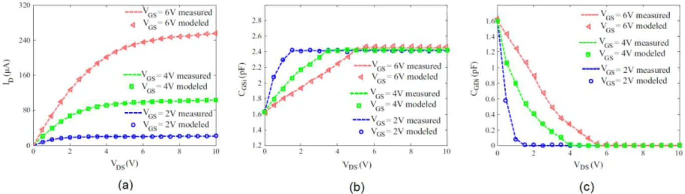
Figure 4.3 shows the measured curves in which the model was based on, as well as the TFT model simulation. As it can be observed, the simulations show a good agreement (<5 % mean absolute relative error) with the corresponding measurements.
These devices are showing a VONof ≈ - 0.5 V, a VTH of 1.35 V, an on/off current ratio
greater than 107 and a mobility around 20 cm2/V.s [29].
Figure 4.3- Verilog-A neural model performance validation from the measurements 0 ≤ VDS ≤ 10 V in steps of 0.5 V and 2 ≤ VGS ≤ 6 V in steps of 2 V.(a)- Output characteristics curvers of the TFT. (b)- C-V characteristics curves between gate and source (CGSi) (c)- C-V characteristics curves between gate
This previously developed model allows to properly simulate the building-blocks in which, all the circuits will have the same fabrication conditions as the TFTs from model.
4.2.1 Logic gates
Inverter
Regarding design, the inverter is one of the simplest but most important circuits in digital electronics domain. In this project, the inverters were designed using a diode-connected load and a driver TFT. The optimized size ratio between the driver and load TFTs to obtain maximum and minimum values of VOHand VOL respectively, and considering a VDD of 10 V, was 4:1. Although,
plenty of ratios were used depending on the final application of the inverter, i.e. if we simply want a signal inversion, or an output voltage regeneration. The simulation of this and other logic gates was done at a frequency of 1 kHz, since the desired operation frequency of the system is in the range of few kHz.
15
Figure 4.5- Layout of the inverter circuit.
In all the simulations the diode-connected transistor is operating in saturation mode (VDS>VGS-VT).
In figure 4.2 it is presented the response of the inverter when a square wave is applied as input, considering a load transistor with W= 20 µm and L= 10 µm and a driver transistor with W=
80 µm and a L= 20 µm, with a VDD= 10 V. Almost full swing of the output from near 0 V to VDD–
VT was observed for all the voltages, specifically presenting a high output voltage of 9 V, and a
low output voltage of 510 mV for a frequency of 1 kHz.
In figure 4.5 it is presented the layout of an inverter, containing all the input and output pads needed for the testing phase.
NAND gate
A NAND gate has been also designed, with two driving TFTs in series and one diode-connected load. This logic gate only has a low output when both inputs are in high state, otherwise if any of the inputs is low the logic gate output will be high.
17
with a VDD=10 V. The simulation was performed applying two pulses as input (Vin1 and Vin2) with
some delay relatively to each other, in order to have all the possible input combinations.
It can be observed on the simulated plots that the logic gate is behaving has expected, having a low output voltage only when the two inputs are high. It was obtained a high output voltage of 9.61 V and 9.92 V (there are two values resulting from the different input combinations that originate a high output voltage) and a low output voltage of 230 mV for a frequency of 1 kHz.
NOR gate
For the NOR logic gate the same simulation conditions were tested, but using two driving TFTs in parallel and diode-connected load with the same dimensions as in the NAND gate. This logic gate only has a high output state when both inputs are low. On the other hand, if one of the inputs is high the output will consequently be low.
The schematic, simulation and layout of this logic gate can be observed in figures 4.6 and 4.7.
Figure 4.9- Layout of the NOR gate circuit.
The expected functionality of the NOR gate was achieved. For a frequency of 1 kHz, it was obtained a high output voltage of 9.82 V and a low output voltage of 230 and 340 mV depending on the different inputs combination that results in a low output value.
Overall, these simulated results demonstrate sharp transfer characteristics and a satis-factory functionality with operating frequencies up to tens of kHz. Although the operating frequen-cies are not as good as some other TFT technologies (particulary poly-Si owing to the intrinsically lower mobility of oxide semiconductors), some optimizations can be realized to allow higher op-erating frequencies, like scaling down the device dimensions, reducing the parasitic capacitances and the interconnections resistance.
Despite that, the TFTs have presented a very satisfactory performance, and viability in digital electronics for flexible and transparent electronic systems.
4.2.2 On-chip clock generator
Ring oscillatorA ring oscillator was designed to produce a square wave signal that will be used as the
system clock. In this electronic block it’s mandatory to always have an odd number of inverters to
obtain an oscillation, otherwise the system would give a stable DC output value.
19
Figure 4.10- Scheme of a 23-stages ring oscillator.
Figure 4.11- 23-stages ring oscillator layout
With this topology and number of stages, a clock signal with an oscillation frequency of 50 kHz has been achieved. However, this frequency value is excessively high for the desired appli-cation, and some non-ideal effects may arise due to the response time of some electronic blocks. By adding more stages to the ring oscillator, it is possible to reduce the output frequency, but not significantly, so in order to decrease this value a frequency divider based on D-type flip-flops has been implemented. The usage of 23 stages in the ring oscillator allow to produce an output fre-quency which is not sufficiently high to degrade the performance of the counter itself, and also we were able to get complete rail-to-rail operation. In addition, with a very low number of stages we start to get a sine wave instead of a square one.
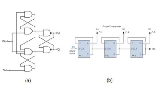
Frequency divider (D-type flip-flop counter)
As aforementioned, a D-type flip flop was design in order to be used as a frequency divider (counter), since the clock signal generated with the ring oscillator had an excessive frequency that could decrease the overall performance. The flip flop schematic and layout can be observed in figures 4.12 and 4.13. The 3-input NAND used, besides having another driving TFT in series with the other two, has the same schematic as the 2-input NAND already described above.
Figure 4.12- (a)- Circuit schematic of a D-type flip-flop. (b)- Scheme of the frequency divider feedback connections using a D-type flip-flop.
21
Figure 4.14- Scheme of the clock generator, comprising the ring oscillator and the 4-bit cou-nter.
Figure 4.15- Simulation result of the 4-bit counter, when the signal generated by the ring os-cillator is given as an input.
The blue line in the simulation represents the clock signal generated right after the ring oscillator, with a frequency of ≈ 50 kHz and the red corresponds to the clock signal after the 4-bit counter where it was achieved a final frequency of 3 kHz (i.e., frequency division by a factor of 16). The clock has a high voltage value of 9.2 V, and a low value of 0.7 V. The slight decay that occurs in the high voltage phase does not affect the circuit performance at all.
4.2.3 Non-overlapping clock-phase generator
Since the capacitance-to-voltage converter needs two different input phases, a non-over-lapping clock-phase generator was also designed and implemented, whose schematic and layout can be observed in figures 4.16 and 4.17. This circuit is composed only by inverters and NOR gates. When a square signal is applied as the input, this block will generate two non-overlapping phases that are commonly used to perform the on/off commutation of transistors that act as switches.
More inverters can be added to the schematic in order to optimize the non-overlapping time.
23
Figure 4.18 presents the phases generated by this block when a non-ideal input is given (i.e. the clock signal generated).
Figure 4.18- Simulation result of the non-overlapping phase generator when the clock signal is given as an input.
The phases have a “ON value” of 7 V and a “OFF value” of 300 mV. However, phase 2 has a little spike that arises from the input clock, but as before, this effect does not degrade the circuit performance since the values are not close to the ones necessary to enable the switches in the OFF state.
It is important to refer that in the cascaded inverters, the width of the driving TFTs was gradually increased by a factor of two, to properly regenerate the output and, simultaneously, increase smoothly the driving capability. Therefore, the widths (W) of the driving TFTs are (from
the first cascaded inverter to the last one respectively) 40, 80, 160 and 320 µm, whereas the length (L) is kept equal to 20 µm to all of them.
4.2.4 Capacitance-to-voltage converter
This block is used to convert the different capacitance values from the sensor (with/with-out water) in readable voltage values that will be used as an input of the comparator.
Figure 4.19- Circuit schematic of the capacitance-to-voltage converter proposed.
In table 4.1 it is presented the charge (Q) in each capacitor in both phase one and two.
Table 4.1- Representation of both capacitors charge in phase one and two.
Phase 1 Phase 2
QCsensor Csensor.(Vref1 - Vref2) (Vout - Vref2).Csensor
QCref 0 (Vout - Vref2).Cref
Knowing that a capacitor charge is equal to his capacitance times the voltage applied at its terminals, and also assuming that, between phase one and two charge conservation occurs, we obtain:
𝑉
𝑜𝑢𝑡=
𝑉𝑟𝑒𝑓1− 𝑉𝑟𝑒𝑓21+𝐶𝑠𝑒𝑛𝑠𝑜𝑟𝐶𝑟𝑒𝑓
+ 𝑉
𝑟𝑒𝑓2 (5)Where Cref, Csensor, Vref1 and Vref2 represent, respectively the capacitance reference value,
the sensor capacitance and the voltage reference one and two.
25
there is water in the sensor allowing to have a capacitance gain of 100 % resulting in a capaci-tance of 10 pF. This capacicapaci-tance variation allows to have an output voltage variation of about 400 mV, yielding a sensibility of ≈ 80 mV/pF.
By means of a parametric analysis, the chosen optimized value for the reference capacitor was 6 pF, since this was the one that could provide the biggest voltage variation at the output for the same sensor capacitor gain.
The layout of this block can be observed in figure 4.21.
Figure 4.20- (a)- Transient simulation result of the C/V converter when there is no water in the capacitive sensor (5 pF). (b)- Transient simulation result of the C/V converter when there is water in the capacitive sensor (10 pF).
The red line represents the reference voltage of the comparator where it can be obviously seen that in the (a) scenario the capacitance-to-voltage converter output is always bellow this value but in the other hand in (b), in phase two, the output has a higher voltage value than the reference.
For the range of sensor capacitance (few pico-faradays) provided by one the project part-ners, a gain of 100 % was considered, i.e. the sensor capacitance goes from 5 to 10 pF, but the full system can discriminate the two different scenarios even with a gain of only 40 %.
4.2.5 Comparator
Latch
Being a latch part of the comparator, a simple one has been designed. It can be seen as a back to back connection of two inverters with positive feedback.
The latch schematic can be observed in figure 4.22 (a). Since the latch output is differential, there is a need to perform a dual to single-ended conversion, in which was used the simple cir-cuitry presented in figure 4.22 (b). By representing the small-signal model of this converter it yields:
𝑉
𝑜𝑢𝑡= 𝑉
𝑖𝑛+− 𝑉
𝑖𝑛− (6)27
The layout of the latch and the doble-to-single ended converter can be observed in figure 4.23.
Figure 4.23- Layout of the latch and the doble-to-single ended converter
Positive feedback amplifier
Instead of using a regular common-source differential amplifier topology, it was adopted a topology that takes advantage of a positive feedback loop to significantly boost the gain. This topology schematic can be observed in figure 4.24 and it was adapted from [31].
Figure 4.24- (a)- Circuit schematic of a regular common source amplifier having a positive feedback unit. (b)- Circuit schematic of the differential amplifier where the feedback network can be observed, adapted from [31].
By drawing the small-signal model of (a), and considering that Af ≈ 1, the gain can be
ex-press by:
𝑉𝑜𝑢𝑡
𝑉𝑖𝑛 = −𝑔𝑚18×(𝑟𝑜18//𝑟𝑜17) (7)
So this topology allows to have a much higher voltage gain when compared to a regular common-source differential amplifier, resulting in a better discrimination, thus a better comparison between similar voltage levels at the input of the comparator (i.e. the comparator have a lower offset voltage).
The main drawback of this topology is the decrease of the amplifier bandwidth, but in
this particular case it doesn’t bring any issues, since in the desired final application a low
opera-tion frequency will be used.
The simulations and the layout of the pre-amplifying block is presented in figures 4.25 and 4.26.
29
Figure 4.26- Layout of the positive-feedback amplifier.
In (a) it is presented the frequency response of the differential amplifier with positive feed-back, where it was possible to achieve an 11 V/V (20.8 dB) gain using 2 V as biasing condition, however the amplifier only present this gain when operating at frequencies in a range of few kilohertz. In (b) the input differential signal has an amplitude of 0.02 V, whereas the resulting output presents an amplitude of 0.22 V, being in accordance with the bode magnitude plot.
Complete comparator
The comparator is composed by a cascade of two positive feedback pre-amplifiers followed by an analog latch. The function of this block is to compare the voltage output value of the capac-itance-to-voltage converter with a given reference, allowing to detect if there is, or not, water in the capacitive sensor.
As above-mentioned, the adopted high gain topology of the pre-amplifiers will help to better discriminate the values between the comparator voltage reference and the capacitance-to-voltage converter output by providing a good amplification between the differential signal.
Figure 4.27- (a)- Simulation result of the comparator output when a differential voltage sweep is applied. (b)- Simulation result of the comparator output when a input triangular signal is applied.
The comparator presents a high output of 6.8 V (logic level “1”) when Vin+ is higher than Vin-, and a nearly zero output in the other case.
It was achieved a good output swing for the desired application, so it is possible to discrim-inate which input of the comparator has a higher voltage value, allowing to directly know if we have, or not, water in the sensor. It was obtained a simulated systematic voltage offset value of 63 mV.
If higher accuracy was envisaged, the number of cascaded pre-amp stages could be in-creased, however, there is a limited active area that is allowed to be used on the bottle, so the increase of the die area must be taken into account.
4.2.6 Low-pass filter
31
Figure 4.28- Circuit schematic of the low pass filter.
The following plot in figure 4.29 shows the frequency response of the low-pass filter. It has an enough cut-off frequency to prevent undesired high frequencies or huge spikes.
Figure 4.29- Bode magnitude plot of the low-pass filter.
4.2.7 Design of the complete system
Figure 4.30- (a)- Result simulation of the final system output when there is not water in the capacitive sensor. (b)- Result simulation of the final system output when there is water in the capacitive sensor.
In (a) it is shown the output signal when there is no water in the sensor (Csensor= 5 pF). The
signal remains stable at about 300 mV, so it will result in the off state of the electrochromic cell. In (b) it is presented the output signal when there is water in the capacitive sensor (Csensor= 10
pF). It can be seen that the output signal oscillates between 4 and 6 V. This oscillation occurs due to the switch after the comparator, which is supposed to sample phase two and hold in phase one but, since there is some circuit delay, it also samples the end of phase one which has a lower voltage. However, this decay does not affect in any aspect the circuit performance, since at these voltage ranges the electrochromic cells used as display elements are already saturated in terms of transmittance change and their response is considerably slower to turn visible any kind of light flickering. However, the output signal can be further optimized be changing the cut-off frequency of the low-pass filter.
33
arise. However, in order to validate all the simulations, the proposed circuits will be fabricated and tested under the same simulated conditions.
4.3 Printed circuit board design
In order to realize the electrical characterization of blocks that need more than five source measure units (SMUs) there is a need to use PCBs to help both in the testing phase, in the debugging and also because the in-house parameter analyzers only have up to four microposi-tioners. All the PCBs were designed in CadSoft EAGLE software and for testing purposes there was also a need to design the layout of a PCI connector in order to make the connection between the substrate of the testing circuit and the respective PCB.
All the individual blocks will be further electrically characterized as well as the total sys-tem, so according to the inputs, outputs and biasing needed to each block, it was inferred that there was a need to design one PCB to each of the following blocks: capacitance-to-voltage con-verter, positive feedback differential amplifier, latch and the smart bottle total system.
Capacitance-to-voltage converter
Figure 7.1 in C annex, shows the schematic and the board of the PCB designed for the C/V converter testing. There was a need to design a circuit that would produce the non-overlap-ping phases for the switches as well as a buffer that allows the output signal measurement with an oscilloscope, since without this buffer the circuit performance would be degraded by the huge capacitance load of the oscilloscope probe.
Positive Feedback Differential Amplifier
The schematic and layout of the PCB designed for the positive feedback differential am-plifier testing are presented in Figure 7.2 in C annex. It was necessary to design a circuit to pro-duce two differential inputs, so two simple operational amplifiers (OPAMPs) inverting and non-inverting schemes were used. Hence, when fed by a wave generator the PCB will produce two perfectly differential waves. In this case we also need buffers at the output of the circuit to meas-ure the signal for the same reason as above mentioned.
Latch
Full system
35
5
Conclusions and Future Perspectives
The work in this dissertation was focused on the development of a fully autonomous elec-tronic system for a smart bottle packaging, taking into account all the circuitry involved for the desired application as well as the building blocks layouts and the auxiliary printed circuit boards to help in the testing phase.
Several building-blocks like a clock generator, a phase generator, a C/V converter and a comparator have been designed, being achieved good functionality and encouraging results for all of them. All the building-blocks can operate up to several tens of kHz, although in the final application a low frequency of operation will be used. Disregarding the clock generator, the sys-tem only comprises the reduced number of 55 TFTs, which is helpful concerning the random fabrication process variations that can occur resulting in device mismatches. In order to guarantee robustness against VON variations, all the system was re-simulated considering a value of 0.5 V
instead of -0.5 V, and good results were also obtained by means of changing only some biasing conditions.
The C/V converter designed has shown to be quite interesting since a good sensibility of about 80 mV/pF was achieved, and a linear transfer characteristic was obtained for a range of few pF, using only a circuit with three TFTs and two capacitors (including the capacitive sensor) based on a charge distribution method, where no amplifying neither frequency or time conversion was used. Further adding up the fact that, no kind of reference was found regarding the use of oxide TFTs in designing any type of C/V converter.
The design and adaptation of the differential amplifier with positive feedback, to the a-IGZO TFT technology, allowed to proof the potential of this topology when a high gain is required in systems with low operating frequencies (since it has the drawback of having a lower bandwidth). Frequently used oxide TFT based differential amplifiers, like the common source topology allows to have gains in the order of 2-3 dB, while with this topology a gain of 20 dB was achieved [32].
Taking into account all the work involved, it is possible to conclude that oxide TFT technol-ogy has a huge and unexplored potential for many other low-frequency applications besides the mainstream and well-known backplanes of transparent displays or radio frequency identification tags (RFID) [33]–[36].
Since the masks layout and the testing PCBs were already designed, the fabrication in clean room environment and further electrical characterization of the whole system will occur during December 2016.
In the project final product, it is also desired to use a-ZTO TFTs instead of the mainstream
a-IGZO due to some of the enhanced chemical and physical properties and the abundance of its
elements in nature, resulting in low price, compared to a-IGZO, and favoring its widespread use. At the moment, one of the main drawbacks of a-ZTO TFTs is the lower electronic mobility when compared to the a-IGZO, but it doesn’t make a huge difference in applications where operating
speed is not such an important factor. Furthermore, owing to the higher electrical resistivity of ZTO compared to IGZO, harder saturation is achieved, resulting in higher intrinsic gain and better flexibility to design analog building-blocks
In the future, the layouts will also be moved from lab-scale processes to semi-industrial roll-to-roll systems (namely sputtering for the oxide semiconductor, atomic layer deposition for the dielectric and printing for the electrodes), allowing to enhance cheap, large scale, and mass pro-duction.
37
6
References
[1] X. Tao and T. Institute, Wearable Electronics and Photonics. Woodhead, 2005.
[2] B. P. Görrn, M. Sander, J. Meyer, M. Kröger, E. Becker, H. Johannes, W. Kowalsky, and
T. Riedl, “Towards See-Through Displays : Fully Transparent Thin-Film Transistors Driving Transparent Organic Light-Emitting Diodes **,” pp. 738–741, 2006.
[3] B. G. Lewis and D. C. Paine, “A pplications and Processing of Transparent,” no. August,
pp. 22–27, 2000.
[4] D. Jin, J. Lee, T. Kim, S. An, D. Straykhilev, Y. Pyo, H. Kim, D. Lee, Y. Mo, H. Kim, and
H. Chung, “Emission AMOLED Display on Plastic Film and Its Bending Properties,” pp.
983–985, 2009.
[5] M. Ito, M. Kon, C. Miyazaki, N. Ikeda, M. Ishizaki, R. Matsubara, Y. Ugajin, and N. Sekine,
“pss solidi,” vol. 1894, no. 8, pp. 1885–1894, 2008. [6] J. F. Wager, “No Title,” vol. 1245, no. 2003, 2014.
[7] E. Fortunato, P. Barquinha, and R. Martins, “Oxide Semiconductor Thin-Film Transistors : A Review of Recent Advances,” 2012.
[8] R. L. Hoffman, B. J. Norris, and J. F. Wager, “ZnO-based transparent thin-film transistors ZnO-based transparent thin-film transistors,” vol. 733, no. 2003, pp. 1–4, 2010.
[9] W. den Boer, Active Matrix Liquid Crystal Displays: Fundamentals and Applications. Elsevier Science, 2011.
[10] A. Chaudhry, M. J. Kumar, A. Chaudhry, and M. J. Kumar, “Controlling Short-channel
Effects in Deep Submicron SOI MOSFETs for Improved Reliability : A Review,” vol. 4, no.
March, pp. 99–109, 2004.
[11] “Plastic transistors in active-matrix displays,” vol. 41, no. 1999, p. 4840, 2001.
[12] R. Martins, C. De Caparica, and E. Fortunato, “Paper Electronics : A Challenge for the Future,” pp. 365–367, 2013.
[13] J. S. Park, T. W. Kim, D. Stryakhilev, J. S. Lee, S. G. An, Y. S. Pyo, D. B. Lee, Y. G. Mo,
D. U. Jin, and H. K. Chung, “Flexible full color organic light-emitting diode display on polyimide plastic substrate driven by amorphous indium gallium zinc oxide thin-film
transistors,” Appl. Phys. Lett., vol. 95, no. 1, pp. 10–13, 2009.
[14] B. G. Gelinck, P. Heremans, K. Nomoto, and T. D. Anthopoulos, “Organic Transistors in Optical Displays and Microelectronic Applications,” pp. 3778–3798, 2010.
[15] J. K. Jeong, D. U. Jin, H. S. Shin, H. J. Lee, M. Kim, T. K. Ahn, J. Lee, Y. G. Mo, and H. K. Chung, “Flexible Full-Color AMOLED on Ultrathin Metal Foil,” vol. 28, no. 5, pp. 389–
391, 2007.
[16] J. S. Discrete, K. Nomura, H. Ohta, A. Takagi, and T. Kamiya, “Room-temperature fabrication of transparent flexible thin-film transistors using amorphous oxide
semiconductors,” vol. 432, no. November, pp. 3383–3386, 2004. [17] B. R. A. Street, “Thin-Film Transistors,” pp. 2007–2022, 2009.
[18] H. T. Transistors and A. S. Films, “High-Performance Thin-Film Transistors in,” no. 8,
1987.
31, no. 11, pp. 1245–1247, 2010.
[20] H. Q. Chiang and J. F. Wager, “High mobility transparent thin-film transistors with
amorphous zinc tin oxide channel layer,” vol. 013503, pp. 22–24, 2005.
[21] K. K. Banger, Y. Yamashita, K. Mori, R. L. Peterson, T. Leedham, J. Rickard, and H.
Sirringhaus, “Solution-Processed Metal Oxide Thin-Film Transistors Formed by a ‘ Sol-gel
on Chip ’ Process solution-processed metal oxide thin-film transistors formed by a ‘ sol – gel on chip ’ process,” no. August, 2016.
[22] D. Marioli, E. Sardini, and A. Taroni, “Measurement of Small Capacitance Variations,” vol.
40, pp. 426–428, 1991.
[23] M. S. Beck, “A High Frequency Stray-Immune Capacitance Transducer Based on the
Charge Transfer Principle,” vol. 37, no. 3, 1988.
[24] A. Arshad, R. Tasnim, A. H. M. Z. Alam, and S. Khan, “Capacitance - to - Voltage Converter Design to Measure Small Change in Capacitance Produced by Human Body
Movement,” pp. 8–11.
[25] B. Chen, “Humidity sensor circuit using real time operating system (FREERTOS) Kernel,”
University of Kentucky, 2014.
[26] S. Shin, Y. You, S. Lee, K. Moon, J. Kim, L. Brooks, H. Lee, and S. Electronics, “A Fully -Differential Zero-Crossing-Based 1 . 2V 10b 26MS / s Pipelined ADC in 65nm CMOS,” pp.
218–219, 2008.
[27] P. E. Allen and D. R. Holberg, CMOS Analog Circuit Design. Oxford University Press, 2002.
[28] R. Barnett and J. Liu, “A 0 . 8V 1 . 52MHz MSVC Relaxation Oscillator with Inverted Mirror
Feedback Reference for UHF RFID,” no. Cicc, pp. 769–772, 2006.
[29] P. Bahubalindrun, V. Tavares, P. Barquinha, P. G. De, and R. Martins, “InGaZnO TFT behavioral model for IC design,” Analog Integr. Circuits Signal Process.
[30] A. P. P. Correia, P. M. C. Barquinha, and J. C. da Palma Goes, A Second-Order $Σ$Δ$
ADC Using Sputtered IGZO TFTs. Springer International Publishing, 2015.
[31] Y. Tarn, P. Ku, H. Hsieh, and L. Lu, “An Amorphous-Silicon Operational Amplifier and Its Application to a 4-Bit Digital-to-Analog Converter,” vol. 45, no. 5, pp. 1028–1035, 2010. [32] A. Correia, R. Martins, E. Fortunato, and P. Barquinha, “Design of a Robust General
-Purpose Low-Offset Comparator based on IGZO Thin-Film Transistors,” pp. 261–264, 2015.
[33] B. Yang, J. Oh, H. Kang, and S. Park, “A Transparent Logic Circuit for RFID Tag in a
-IGZO TFT Technology,” vol. 35, no. 4, pp. 610–616, 2013.
[34] W. Operation, “Oxide TFT Rectifier Achieving 13.56-MHz Wireless Operation,” vol. 59, no.
11, pp. 3002–3008, 2012.
![Figure 2.1- Scheme of the most conventional TFT strutures, according to the position of the gate electrode and sorce/drain electrodes relatively to the semiconductor, adapted from [7]](https://thumb-eu.123doks.com/thumbv2/123dok_br/16692388.743695/26.892.264.694.351.632/conventional-strutures-according-position-electrode-electrodes-relatively-semiconductor.webp)
![Figure 2.3- Voltage transfer characteristic of a comparator with infinite gain, adapted from [27]](https://thumb-eu.123doks.com/thumbv2/123dok_br/16692388.743695/30.892.270.595.557.772/figure-voltage-transfer-characteristic-comparator-infinite-gain-adapted.webp)