Abstract—The paper describes analysis of nonlinear effects in a
MOS transistor operating in moderate inversion and saturation. The dependence of the drain current on the gate-source and drain-source voltages is described using a modified version of the “reconciliation” model developed by Y. Tsividis. In the new model the current components, which correspond to the terms depending exponentially on normalized gate-source or drain-source modulating sinusoidal voltages, are presented using modified Bessel functions. This approach allows one to find the first, second and third harmonics of the drain current caused by the gate-source or drain-source voltage sinusoidal modulation, and find also the intermodulation terms produced by these two modulating voltages. The results are applied to set the requirements to the gate-source and drain-source bias voltages in design of low-distortion and/or low-voltage amplifiers. It is shown that the realization of the stage with the zero value of third order harmonic requires extremely tight tolerances for the threshold voltage. The suppression of intermodulation terms requires increased drain-source voltage. These recommendations are confirmed by simulations.
Index Terms—MOS transistor model, moderate inversion,
saturation, drain current harmonics, low-distortion/ low-voltage amplifier.
I. INTRODUCTION
s anticipated over 30 years ago [1], MOS transistor moderate inversion is an increasingly important region for modern analog circuit design. It provides the best compromise in terms of consumption and speed, especially in low power and low voltage applications.
A very powerful method of analysis and design of linear analog integrated circuits with transistors operating in moderate inversion was described in [2]. This work initiated the analysis of many aspects [3-9]: voltage gain, thermal noise, and settling time of low power/low voltage amplifiers. Yet, in this development, due to the exponential dependence of the drain current on the gate-source voltage, the weak and moderate inversion regions were generally dismissed for low-distortion This work was supported by the NSERC, Canada, by the Portuguese Foundation for Science and Technology (PESTOEEEI/UI0066/2015), and by the Academy of Finland.
I.M. Filanovsky is with the University of Alberta, Edmonton, Canada ([email protected]).
L.B. Oliveira is with the Universidade Nova de Lisboa, CTS-UNINOVA Caparica, Portugal, N.T. Tchamov is with the Tampere University of Technology, Finland.
applications [10] even though some properties of MOS transistors seemingly useful for design of low-distortion amplifiers were found in the course of years.
It was discovered in measurements [11] that when the gate-source voltage is modulated by a sinusoidal signal, the third harmonic of the drain current depending on bias may have two zero values. Other simulations and measurements [12] on the modern sub-micron devices suitable for RF applications indicated a significant peaking, or “sweet spot”, in the third-order intercept point, IP3, for the moderate inversion region. This gave a hope [12] that “a significant increase in linearity with low power consumption is possible”. Finally, the simulation of the drain current in a low-distortion amplifier [13] indicated that this “sweet” point may exist for IP2 as well. Yet, these results cannot be directly applied to design of low-distortion amplifiers. The model which allows one to connect the transistor bias and the regions of operation with calculation of harmonic distortions was absent. The gm/ID characteristic so successfully used in design of linear circuits [14, 15] is not fully adapted for analysis of nonlinear distortions [16-18], because of the limitations occurring when Taylor series’ are used for nonlinear circuit design (a good example is dependence of the ‘sweet spot” on the signal strength overlooked in [12]). The Bessel functions used in this paper help to see better the effects when large amplitude sinusoidal signals are applied.
The first step in this direction was done in [19] where the authors tried to use the so-called ‘reconciliation’ model [20] for this purpose. But this approach, besides of being indirect (via the transconductance derivatives), was still used for evaluation of distortions in small-signal operation. Yet, many features of nonlinear behavior in this case are lost, for example, the dependence of performance on the signal strength when the signal may change the bias voltage.
The goal of this paper is to introduce further modifications of ‘reconciliation’ model which result in using exponential and algebraic terms only. In this case, one can use the modified Bessel functions for calculation of harmonics. The analysis of third and second harmonic suppression follows. Using full modified “reconciliation” model allows one to calculate the intermodulation harmonics, and this is important for design of low-voltage amplifiers. The approach becomes suitable for analysis of wide range of nonlinear effects (some are included).
Using Modified Bessel Functions
For Analysis of Nonlinear Effects
In a MOS Transistor Operating in Moderate Inversion
I.M. Filanovsky, L.B. Oliveira, and N.T. Tchamov
In Section II we are giving a review of this new model and describing its further development for moderate inversion and strong saturation. We also give a clear distinction between the proposed model and the model used in gm/IDapproach. Section III describes the basic properties of modified Bessel functions required for calculations of harmonics. Section IV describes the harmonics due to the gate-source or drain-source modulations and the intermodulation harmonics occurring when both voltages are modulated and provides the formulas for harmonics calculation. Section V provides an example of harmonics calculations for common-source stage and establishes how the achievable reduction of the third or second harmonic is connected with tolerances of the transistor threshold voltage and gives recommendations on the choice of gate-source bias voltage. Section VI describes the influence of the drain modulation on the choice of the drain-source voltage. Section VII gives the application of the harmonics calculation to calculation of 1-dB compression point and shows how using Bessel functions clarifies two-tone test. Section VIII discusses the results and provides some conclusions.
II. NEW TRANSISTOR MODEL
In the “reconciliation” model [20], the drain current IDof an n-channel transistor without body effect is described by the following equation t DS TH GS t TH GS n nV V V n V V Z D I e e I ln2 1 2 ln2 1 2 . (1)
where IZ 2
C'ox(W/L)n
t2,
t (kt)/q is the thermal voltage and VTHis the threshold voltage. The substrate factor n will be approximated as [20]: n1[/
2 VSB2F
] where
is the body-effect factor and
Fis the Fermi voltage. In the model (1), all voltages are taken with respect to the source. The term involving only the gate-source voltageVGS (inversion term) is conveniently separated from the term including bothVGS and the drain-source voltage VDS(saturation term). The model (1) usually (for wide and long transistors) provides a good correspondence between theoretical, simulation and experimental results [21-22] in typical CMOS technologies. If the saturation term can be neglected (VDSis sufficiently high), the current can be approximated as2 2 ln 1 GS TH t V V n D Z I I e (2)
From (2) one can obtain that
/ / 1 D z z D m I I D t I I g I n e (3)
where gm ID/VGS. The eq. (3) is the basis for the above
mentioned [2]gm/ID design approach (we are using in (3) slightly different current normalization).
Both (1) and (2) are not well adapted for the analysis of nonlinear distortions when VGS andVDShave the sinusoidal components. Two expansions of logarithmic functions into series’ are convenient for further derivation. These are [23]
2 2 1 ( 1) ( 1 ) ln ( ) ln( 1 ) k k k x x x k (4) for | 1 x| 1, and 2 2 1 ( 1) ( 1 ) ln ( ) k k k x x k (5) for | 1 x| 1 . Then, using two terms of (4) with
2 1 GS TH t V V n x e
and two terms of (5)
with 1 2 GS TH DS t V V nV n x e
(with modified coefficients
1and 2
of second terms; the details can be found in [21]) one can find the modified model for the region of moderate inversion (VGS VTH) and saturation (|VGSVTH| | nVDS| ) as 2 2 1 2 2 2 2 1 GS TH GS TH t t GS TH DS GS TH DS t t V V V V n GS TH n t DMS Z V V nV V V nV n n V V e e n I I e e (6)where
1 (1 ln 2) and
2 1 (ln 2)2 . The subscripts in DMSI mean the Drain current for Moderate inversion and Saturation (we suggest that the condition (2) is called “Deep saturation”).
Here the model (6) is even further simplified. The terms with 1
and
2 are omitted, and the model is reduced to 2 2 2 GS TH GS TH DS t t V V V V nV n GS TH n DMS Z t V V I I e e n (7)The omitted terms provide a continuous and smoother connection between the adjacent regions of operation (weak, moderate and strong inversion, different degrees of saturation). They do not change the techniques of harmonic calculations (the removed terms are also exponential); but the results with inclusion of these terms will be more cumbersome and does not improve comparison with simulations.
The first two terms of (7) (with their sum squared) describe the transition from moderate to strong inversion [21]. The third term is calculated for |VGSVTH| | nVDS| for the operation in (say, strong) saturation. This term may be used to calculate
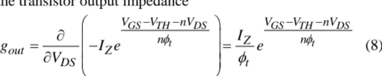
the transistor output impedance GS TH DS GS TH DS t t V V nV V V nV n Z n out Z DS t I g I e e V (8)
One can develop the expression for gout/IDwhich can be used in calculation of nonlinearities as well. This topic is outside the scope of this paper.
The velocity saturation is neglected in both models (1) and (7) and can be considered in the same way as it was considered in [20] for model (1), i.e. by inclusion of a channel-length modulation multiplier.
Here (7) is used for calculation of harmonics in the common-source (CS) stage (Fig. 1), and the voltages
GS
V and VDS may have sinusoidal
componentsvgs Vgmcost andvds Vdmcost.
M
NI
DMS VgsV
DS0V
GS0 VdsFig. 1 Common-source stage with gate and drain modulation
III. MODIFIED BESSEL FUNCTIONS
The calculation of harmonics using modified Bessel functions is based on the following [24] mathematical identities:
1 0 cos ( ) 2 ( )cos n n t x I x I x n t e (9) and 1 0 cos ( ) 2 ( 1) ( )cos n n n t x I x I x n t e (10)
Here I0(x),I1(x),...,In(x)are modified Bessel functions of the first kind [24, 25, and 26]. In MATLAB routine they are available using script besseli(n,x); otherwise they can be calculated using the following series [24]
... ) 3 ( ! 2 ) 2 / ( ) 2 ( ! 1 ) 2 / ( ) 1 ( ) 2 / ( ) ( 4 2 n x n x n x x I n n n n (11)
where(k)(k1)!is gamma-function for positive numbers. The approximate expressions for the values of x 1 are
2 3 2 3 0( ) 1 , ( )1 , 2( ) , 3( ) 4 2 16 8 48 x x x x x I x I x I x I x (12) (in general, ! ) 2 / ( ) ( n x x I n
n (forn1)). The approximations (12) are sufficient to avoid the assumptions of signal smallness in the considered electronics problem. An extensive table of
these functions can be found in [24]. The relative values of higher order functions for the same value of x are quickly decreasing with respect to I0(x) when the order n is increasing (a useful property to remember for evaluation of the dominant intermodulation harmonic).
IV. CALCULATION OF DRAIN CURRENT HARMONICS Let the gate-source voltage include a sinusoidal component, i.e. VGS VGS0Vgmcost . Then one can introduce the normalized variables of t TH GS n V V X
2 0 and t gm n V x 2 . In a similar fashion, if the drain-source voltage also includes a sinusoidal component, i.e.VDS VDS0Vdmcost, one canintroduce the normalized variables of
t DS TH GS n nV V V Y
0 0 and t dm V y . Then, using these normalized variables one can rewrite (5) as
2 ( cos ) 2 cos cos X x t DMS Z Y x t y t X xco t e I I e (13)Using the approximations cos 0 1 2 3 ( ) 2 ( ) cos 2 ( ) cos 2 2 ( ) cos 3 x t e I x I x t I x t I x t
, (14) 2 cos 0 1 2 3 (2 ) 2 (2 ) cos 2 (2 ) cos 2 2 (2 ) cos 3 x t e I x I x t I x t I x t
, (15) and cos 0 1 2 3 ( ) 2 ( ) cos 2 ( ) cos 2 2 ( ) cos 3 y t e I y I y t I y t I y t (16)one finds that
D DMS G DMS DMS I I I , , (17) Here the term
] 3 cos ) 2 ( 2 2 cos ) 2 ( 2 cos ) 2 ( 2 ) 2 ( [ ] 3 cos ) ( 2 2 cos ) ( 2 cos ) ( 2 ) ( [ ) cos ( 2 cos cos 2 3 2 1 0 2 3 2 1 0 2 2 2 , t x I t x I t x I x I e t x I t x I t x I x I e t x X t x t Xx X I I X X Z G DMS (18) defines the harmonics of current caused by modulation of the gate-source voltage only, and which do not depend on the saturation term, and
t y I t y I t y I y I t x I t x I t x I x I e I I Y Z D DMS 3 cos ) ( 2 2 cos ) ( 2 cos ) ( 2 ) ( 3 cos ) 2 ( 2 2 cos ) 2 ( 2 cos ) 2 ( 2 ) 2 ( 3 2 1 0 3 2 1 0 , (19)
modulation is added. Continuing calculations one arrives to the following four groups of harmonics
0 1 2 3
0 1 2 3
1 2 3
cos cos 2 cos 3
( cos cos 2 cos 3 )
( cos cos 2 cos 3 )
( ) DMS Z Z Z Z I I A A t A t A t I B B t B t B t I D t D t D t I IMH (20)
We are using below the values of harmonics amplitudes normalized by the currentIZ. The first group of harmonics are produced by the modulation of gate-source voltage only. Their normalized values are the following
) 2 ( ) ( 2 ) ( 2 2 0 2 1 0 2 2 0 x I e x I xe x I Xe x X A X X X , (21) ) 2 ( 2 )] ( ) ( [ 2 ) ( 4 2 1 2 2 0 1 1 x I e x I x I xe x I Xe Xx A X X X (22) ) 2 ( 2 )] ( ) ( [ 2 ) ( 4 2 2 2 3 1 2 2 2 x I e x I x I xe x I Xe x A X X X (23) ) 2 ( 2 ) ( 2 ) ( 4 3 2 2 3 3 Xe I x xe I x e I x A X X X (24)
The second group has the normalized amplitudes
)]; ( ) 2 ( 2 [ )]; ( ) 2 ( 2 [ )]; ( ) 2 ( 2 [ )]; ( ) 2 ( [ 0 3 3 0 2 2 0 1 1 0 0 0 y I x I e B y I x I e B y I x I e B y I x I e B Y Y Y Y (25) They appear when both gate and drain modulations are present. For the amplifiers, the value of Y is negative; the region of
saturation requires that nVDS0 VGS0VTH and increasing VDS0 suppresses these harmonics (see Sections
V and VI below). In case of the gate-source modulation only they should be considered when VDS0 is small (low-voltage power supply). Then, using (25), one must putI0(y)1. The third group of harmonics appears also when the both the gain-source and drain-source modulations are present. The normalized harmonics amplitudes in this case are
)]; 2 ( ) ( 2 [ )]; 2 ( ) ( 2 [ )]; 2 ( ) ( 2 [ 0 3 3 0 2 2 0 1 1 x I y I e D x I y I e D x I y I e D Y Y Y (26) In case of drain-source modulation only one has to put
1 ) 2 (
0 x
I in calculations using (26). These components are also important in case of small values ofVDS0, and are suppressed increasing VDS voltage (see Sections V and VI below again).
Finally, the last group, the normalized intermodulation harmonicsIMH, are obtained from the expression
1 2 3 1 2 3 [2 (2 ) cos 2 (2 ) cos 2 2 (2 ) cos 3 ][ 2 ( ) cos 2 ( ) cos 2 2 ( ) cos 3 ] Y e I x t I x t IMH I x t I y t I y t I y t (27)
Using the tables in [24] or graphs in [26] one can find that the
functionI1(x)increases faster thanI2(x) orI3(x) (see also remarks under eq. (12)). Hence, the intermodulation harmonics obtained from multiplication of the first terms in the square brackets of (27) 1 1 2 Y (2 ) ( ) cos( ) IMH e I x I y
t (28) and 1 1 2 Y (2 ) ( ) cos( ) IMH e I x I y
t (29) have usually the largest amplitudes.Table I. Intermodulation Harmonic Coefficients
t
cos cos2t cos3t
cos t 2I1(2x)I1(y) 2I2(2x)I1(y) 2I3(2x)I1(y)
cos 2 t 2I1(2x)I2(y) 2I2(2x)I2(y) 2I3(2x)I2(y)
cos 3 t 2I1(2x)I2(y) 2I2(2x)I3(y) 2I3(2x)I3(y)
All other intermodulation harmonics can be obtained from (27) using the formulas of elementary trigonometry. It is convenient to use Table I; the multiplier e and the signs of the Y
terms in the table are omitted. Yet, this multiplier indicates us that these harmonics can also be suppressed increasing the VDS voltage (see Section VI again).
V. THIRD AND SECOND HARMONICS AND CSSTAGE BIAS In this part we consider calculations of harmonics for the transistor designed for 65 nm technology. The basic parameters of this technology are the following: VTH 0.24 V,
ox C
983 µA/V2 (extrapolated from the data in [22]), thesubstrate factorn1.3, and the thermal voltage
t 25.9 mV. The simulations are done for the device with the aspect ratio
L
W / 50µm/0.36µm. This gives the normalizing current of
Z
I 238 µA. The simulation dependencies considered in this part are obtained using the drain-sourceVDS 1V (nominal voltage for this technology).
Assume that there is no drain modulation. The design of a low-distortion amplifier with low-power dissipation is, first of all, connected with searching the optimal bias point located in the region of moderate inversion and minimizing the third harmonic. Let us see how the third harmonic of current is varying when the bias voltage VGS0is changing. The eq. (7), with omitted saturation term, is describing the transition from moderate (exponential term in the first bracket of (7) is dominating) to strong inversion (the algebraic term is dominating). The border,VGST , between these two regions can be found from the equation
X
eX (30) The solution of (30) is X 0.567which gives VGST 0.278 V ≈ 0.3 V. Hence, below this voltage the transistor operates definitely in moderate inversion.
3 2 X[ 2 3( ) 2( ) X 3(2 )]
A e XI x xI x e I x (31) Calculating |A3|as a function of the bias voltage VGS (Fig. 2) for the above mentioned process parameters one observes that there are, indeed, two bias points where this harmonic becomes equal to zero. To find these points one has to solve the nonlinear equation
3 2 3
2XI ( )x xI ( )x eXI (2 )x 0
(32)
Fig. 2 Calculation of normalized third harmonic
The left side of (32) is a function of both X(i.e. bias) and
x (i.e. signal amplitude). Yet, one can separate these variables
using approximations (12). Substituting them into (32) one finds that 3 3 3 ( 3 4 ) 3( ) 12 X X x e A X e x F X (33) where F X3( )[eX( X 3 4eX)] /12 can be called the third harmonic distortion factor. Hence, if one chooses the bias voltage at the points defined by the equation
3 4 X 0
X e
(34) the third harmonic amplitude becomes zero. The solutions of (34) are X 1 0.451 (corresponding to VGS10.270 V) andX 2 2.742 (corresponding to VGS2 0.425V).
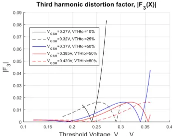
The first point is definitely located in the region of moderate inversion. To estimate the suitability of this point for biasing of a low-distortion amplifier, let us remark that using the bias voltage of VGS00.270 V for moderate inversion means that this voltage is always larger than the threshold voltageVTH. This requires an unrealistically tight tolerance of 10% forVTH. Fig. 3 shows how the value of |F3|changes when, with a given bias voltage, VTHvaries within chosen tolerance. Then, for the tolerance of 10%, 0.216 VVTH 0.268 Vand, indeed, for the case of VTH 0.24 Vand VGS00.270 V(Fig. 3, black line) the amplitude|F3|is equal to zero. But if VTHis close to 0.268 Vthe amplitude of|F X3( ) | is quickly increases (read:
Fig. 3 Bias voltage and threshold voltage tolerances
the third harmonic distortion increases tremendously).
Similar observations should be done for other choices of the bias voltage. Using VGS00.320 Vrequires 25% tolerance for
TH
V . Then0.18 VVTH 0.30 V, and if VTH satisfies this condition, the maximal value of |F3 max| 0.0162 located between X1 and X2. If the tolerance even wider (say, 50%, which is very realistic), i.e. 0.12 VVTH 0.36 V, then, using
0 0.37 V
GS
V may give the increased values of
3 3 max
|F | |F | for transistors with high values of VTH (Fig. 3, blue line). Increasing the bias voltage one can finally find the bias voltage VGS0 0.385 V(Fig. 3, red line) which provides the value of |F3| which is not exceeding the value of|F3 max| 0.0162for the whole possible range of VTH voltage.
Hence, Fig. 3 is the most important plot for the low-distortion one-transistor amplifier design. One concludes that using the first zero solution of (34) is practically impossible; it is better to rely on the value of the distortion factor|F3 max| 0.0162. Further increasing the bias voltage decreases |F3|(see the result forVGS00.425 V). But now the transistor dissipates more power, and the result is not so spectacular: the curve of |F3| around maximum is rather flat. Now consider the contribution B3 to the third harmonic (see (25)). If the drain voltage modulation is absent, one has to use
0( ) 1
I y in calculation of this component. Then, using the approximation for I3(2 )x from (12) one obtains
3 3 Y( / 3)
B e x (35) If it is desirable to suppressB3with respect to A3 one can introduce and specify the suppression coefficient
3dg | 3| / | 3|
S B A (36) Then, from (33) and (35) one finds that the required drain-source bias,VDS0, can be obtained from the equation
3 max 3 3 | | Y
dg
e F S (37) We remind thatY(VGS0VTHnVDS0) / (n
t), then, to be on a safe side, one has to use the lowest value of VTHin the calculations of 0 0 3max 3 ln(3 ) GS TH DS dg t V V nV Y F S n
(38)For example, for the considered case with
0 0.385 V
GS
V one must use VTH VTHmin 0.120 V (minimal value of the threshold voltage in case of 50% tolerance). Then, to obtain S3dg 0.01 one finds that the required drain-source bias voltage VDS0 0.257 V. This voltage is higher than (0.385-0.260) V=0.125 V which would be required to keep the transistor in saturation for the nominal value of the threshold voltage.
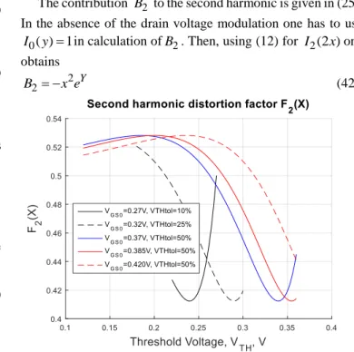
The evaluation of the second harmonic can be done in the same order which we used for the third harmonics. The eq. (23) can be rewritten as 2 2 2 1 3 2 2 {2 ( ) [ ( ) 2 ( )] (2 )} X X x A e XI x x I x I x e I x (39) Fig. 4 shows the dependencies of A2 from VGS0, the bias voltage, and for the same signal amplitudes as in Fig. 3. Then, indeed, one can find the bias voltage for which the value ofA2is minimal.
Using (12) one finds that eq. (39) can be reduced to
2 2 2 2 1 ( 2 2 2( , ) 2 12 X X x x A e X e x F x X (40)
The multiplier F x X2( , )practically does not change for the signal amplitudes shown in Fig. 4, i.e. one can write that
2 2 1 ( , ) ( ) 1 2(1 ) 2 X X F x X F X e X e (41) The function F X2( )has the minimum of F2 min( )X 0.412 located at X 0.450corresponding to VGS00.270 V, andFig. 4 Normalized second harmonic as the function of bias voltage
the flat maximum of F2max( )X 0.528which is located at 2.670
X corresponding to VGS00.420 V.
Usually, the main goal is minimization of the third harmonic amplitude|A3| (with simultaneous minimization of power dissipation). But if it is required to evaluate a possible minimization of A2 one has to connect it with the VTH tolerances, as it was done previously.
Fig. 5 shows that the minimal value of 2 min( ) 0.412
F X can be realized for a very narrow range of TH
V tolerances (even less than 10%); yet, the result will be only about 20% better than for the case of 50% tolerance. The only satisfying conclusion is that F2max( )X 0.528 practically does not depend on bias in the range important for minimization of|A3|.
The contribution B2 to the second harmonic is given in (25). In the absence of the drain voltage modulation one has to use
0( ) 1
I y in calculation ofB2. Then, using (12) for I2(2 )x one obtains
2
2 Y
B x e (42)
Fig. 5 Bias voltage and threshold voltage tolerances
To quantify the suppression of this contribution, one can introduce and specify the suppression coefficient
2dg | 2| / | 2|
S B A (43) If the choice of VGS0is defined by conditions of design for the third harmonic, then one can consider that
2
2 2 max
A x F and calculate 2dg Y / 2 max
S e F (44)
Using (44) and the definition of
0 0
( GS TH DS ) / ( t)
Y V V nV n
one can find the required drain-source bias voltage,VDS0, from the equation0 0 2 2 max ln( ) GS TH DS dg t V V nV S F n
(45)To be on a safe side one must use
min 0.120 V
TH TH
V V again in this calculation.
As follows from the above given analysis the choice of gate-source voltage for a low-distortion stage operation can be summarized the following way.
Fig. 6 Dependence of the third harmonic on bias voltage, Vgm=2 mV
The designer should assume that the first “sweet” point for the third and the “sweet” point for second harmonics require too tight tolerance forVTH. From the other side, the bias voltage located between the “sweet” points of the characteristics shown in Fig. 2 and corresponding to the maximum value of
3 max
|F X( ) | may provide a reasonable bias voltage at the condition that the corresponding level of the third harmonic and power dissipation are acceptable.
The most important parameter for the design is the threshold voltage: its nominal valueVTH , and its tolerance, i.e. the maximum,VTHmax, and minimum,VTHmin, values (these two figures are usually difficult to provide). Then, using the nominal value of VTHone has to find the value of Xcorresponding to
3( ) [ X( 3 4 X)] 0.0162
F X e X e (46) The solution of this equation isX 0.971, and the bias voltage corresponding to this normalized value is VGS 0.31 V(all calculations are done forVTH 0.24 V, n1.3, and
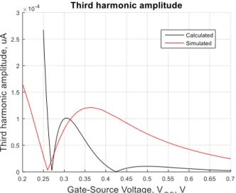
t 25.9 mV). At this stage it is reasonable to simulate the stage using the device with the dimensions satisfying the condition of Y. Tsividis’ model (avoiding short and narrow channel effects) and carrying the current which will be used in the application. An example of such characteristic is shown in Fig. 6. The denormalized value of calculated current is obtained using the normalized values of Fig. 2 and multiplying them by 238 µA, the simulated values are obtained measuring the voltage drop at 1 Ω resistor inserted in the drain circuit. Both the calculated and simulated characteristics are presented forVgs2 mV. One can see that the simulated “sweet” point is sufficiently close to the calculated one. The point of the maximum is located at0.36 V GS
V which is also sufficiently close to the just
calculatedVGS 0.31 V. The second “sweet” point is not pronounced (it exists, but is located at much higher gate-source voltages), yet this is not so important. We know that we have to take the gate-source voltage around VGS 0.35 Vand after that the only way to reduce the third harmonic is to increaseVGS moving towards the second “sweet” point. A better choice would be 0.42 V or larger value (with higher power dissipation). The tolerances for VTHare usually not known. Yet, it is well known that VTHdepends on the channel length. One way to evaluate the influence of VTH variation is to shorten simultaneously the width and the length of transistor. This does not change the parameterIZ, so the calculated characteristic will be the same. But the simulated characteristics can change drastically. Fig. 7 shows the result when the width and length both are shortened by two times. The location of the first “sweet” point is about 0.31 V now. And the maximal value is moved to 0.42 V. Hence, this simulation confirms once more that to rely on biasing in the “sweet” point is not advisable. Then, using the chosen bias (in our case 0.42 V) one must verify that this point is tolerant with respect to the variation of the drain voltage, temperature and process variations (corners).
Fig. 7 Dependence of the third harmonic on transistor length, Vgm=2 mV
Then, if the requirements to the suppression of the harmonics components connected with the variation of the saturation part of the model are given, one has to correct (read: to increase) the drain-source bias voltage.
This, in general, finishes the recommendations on the common-source stage design.
VI. INTERMODULATION
The simulation dependencies considered in this section are obtained for non-standard VDS voltages (below 1 V). The
increase of this voltage mentioned before was a mean to suppress the variation of the saturation part of the model. The presence of drain modulation, as shown in Fig. 1, changes the calculation of these components the following way. Using the approximations (12), with y 0and this modulation signal which is comparable in amplitude with the input signal x
one obtains that
2 2
2 2
|B |e xY ; |D |eY(y / 4) (47) so that the total value of this second harmonic component
becomes 2 2 2 2 2 2 | | | | 1 4 4 dg Y y Y K B D e x e x (48)
Here Kdg |y| / | |x . In a similar way one obtains that
3 3
3 3
|B |eY(x / 3); |D |eY(y / 24) (49) The total value of this third harmonic component becomes
3 3 3 3 3 3 | | | | 1 3 24 3 8 dg Y x y Y x K B D e e (50) One can see that the presence of drain modulation, in case of high level of modulating signal can be also taken care of by increasing the suppression coefficients S2dg and S3dg , i.e. increasing the drain-source voltage.
Table II Values of intermodulation coefficients
t
cos cos2t cos3t
cos t xy 2
(x y) / 2 (x y3 ) /12 cos 2 t (xy2) / 4 (x y2 2) / 8 (x y3 2) / 24 cos 3 t 3
(xy ) / 24 (x y2 3) / 48 (x y3 3) /144 The suppression of intermodulation harmonics is achieved in the similar way. Table II gives the values of the intermodulation coefficients when the approximations (12) are used for the entries in Table I. Recurring to these approximations allows one to evaluate the dominant intermodulation term very quickly: for the same level of the input signal and drain modulation it will be the upper left corner. If the requirement to the suppression are formulated (say, with respect (to the level of gate-source modulation) one can define the required drain-source voltage increase using the same type of calculation as was used for the drain modulation suppression.
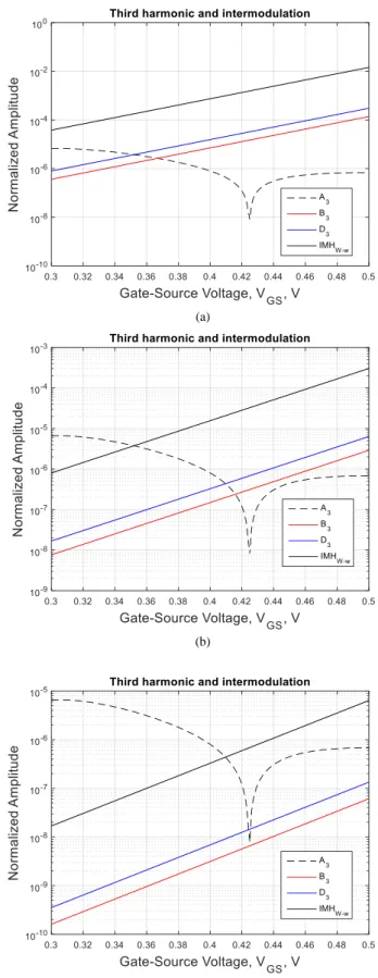
The harmonicA3, in accordance with eq. (25) does not depend on VDSvoltage; but the harmonics B3andD3, and, especially, all intermodulation harmonics strongly depend on this voltage. To demonstrate this dependence, Fig. 8 comparesIMH (black line), B3(red line), D3(blue line), and A3(dashed line). All are normalized values obtained for
5 mV
gm dm
V V .
Let us consider the range 0.32 VVGS 0.40 V which is preferable for low distortion amplifier.
Fig. 8 a) is calculated forVDS 0.2 V. For this drain voltage, with VTH 0.24 Vand n 1.3, transistor will work in saturation. But for these voltages, the intermodulation distortion is strongly dominating (it may have the amplitude which is one
(a)
(b)
(c)
Fig. 8 Comparison of intermodulation amplitude with third harmonic and its components: a) VDS=0.2 V, b) VDS=0.3 V, c) VDS=0.4 V
order of magnitude higher than that of|A3| ), and even components B3 and D3have the amplitudes which may be higher than that ofA3. This means that, even in the absence of
the drain-source modulation, they may define the choice of DS
V voltage. To reduce the level of the intermodulation harmonic to that of A3 one must increase the drain-source to
0.3 V DS
V (Fig. 8 b)). And only when the drain-source voltage is increased to VDS 0.4 V (Fig. 8 c)) the intermodulation harmonic becomes lower than A3 and one can neglect the components B3 andD3.
The diagrams of the Fig. 8 can also be interpreted the following way. The third harmonic components B3 and D3 and intermodulation current IMH are completely suppressed when the drain-source voltage increases further. But the third harmonic A3 does not depend on this voltage. Let us look now at the results of simulation at one particular case of gate-source voltage.
Table III shows the result of simulation for the transistor 50um/0.36um with VGS 0.35 V and modulation signals
5 mV gs
V ( f 100 MHz ) and
5 mV ds
V ( f 110 MHz). One can see that, indeed, the third harmonic, at VDS 0 . 3becomes V close to
3 Z 3 1.6 nA
I I A (this figure can be verified using Fig. 6 and multiplying the value for VGS 0.32 V by 2.53=15.6), then
slowly increases with the growth of the drain-source voltage. But I10MHzis, first, dominating I3below VDS 0.3 V and, second, arrives to its final “asymptotic” value instead of being further suppressed, when VDSbecomes about 0.5 V.
Table III Suppression of harmonics DS V , V 0.2 0.3 0.4 0.5 0.6 0.7 3 I , nA 3.77 1.40 1.44 1.50 1.60 1.69 10MHz I ,nA 285 96.0 90.6 88.7 87.4 86.4
This “asymptotic” value, in accordance with the used model, does not exist, and one can verify that the values for
10MHz
I shown in the Table III forVGS values below 0.3 V are much higher than that calculated in accordance with the model. The proposed simplified model does not provide correct level of intermodulation distortion: it does not indicate the drain-source independent “asymptotic” value of this distortion. This limitation can be corrected using the multiplier representing the channel length modulation factor as it is proposed in [20]. This multiplier, in the analysis of harmonic distortions, will provide the term required for non-attenuated intermodulation distortion. The complexity of derivation will increase, yet this derivation will be “doable’ considering the results obtained already in this paper. This could be the matter of further development.
VII. OTHER APPLICATIONS
a) 1-dB compression point
The obtained expressions for harmonics allow to evaluate one important parameter, the so-called 1-dB compression point. The total first order harmonic of the drain current is given by
1 1 1 0 2 2 1 1 0 2 4 ( ) 2 [ ( ) ( )] 2 (2 ) [2 (2 ) ( )] X X X Y A B Xx Xe I x xe I x I x e I x e I x I y (51)
Consider 2 X as a linear gain. Then, in the absence of the drain-source modulation,I0( )y 1, and the normalized bias
1
X . This allows one to write that
2
1 1 2 2 1(2 ) [2 2 (1 )]
2
Y Y x
A B Xx e I x X e x (52) Then the input signal creating 1-dB compression point can be
found from the expression
2 1.122 (1 / 2) Y X X e x (53) Normally, Yis negative. But if it close to zero (low VDS) , the signal x creating 1-dB compression point is decreasing.
b) Two-Tones Intermodulation Test
The two-tone intermodulation test for evaluation of nonlinearity in narrow-band amplifiers consists of introducing two sources of the same amplitude but with different and close frequencies in the input circuit and finding the terms defining the intermodulation.
Choose the stage size using (3) as in gm/IDdesign method. Then, one can return back to (2) and find the currentID. LetVGS VGS0Vgmcos1t V gmcos2t . Doing the same normalization as in Section IV one can write
1 2 2 1 2 ( cos cos ) cos cos DMS Z X x t x t X x t x t I I e (54) Let the bias is chosen so that (54) can be approximated as
1 2 2 1 2 ( cos cos ) 1 2 ( cos cos ) 2( cos cos ) DMS Z X x t x t I I X x t x t X x t x t e (55)
Now one can use the expansion (15) and write 2 1 2 1 2 0 1 1 2 1 0 1 2 2 2 ( cos cos ) 2 ( cos cos )[ ( ) 2 ( ) cos 2 ( ) cos 2 ][ ( ) 2 ( ) cos 2 ( ) cos ( )] DMS Z X Z I I X x t x t I e X x t x t I x I x t I x t I x I x t I x t (56)
From this expression one can choose the terms which provide the most dangerous intermodulation components.
2 1 2 1 2 1 2 1 2 0 2 1 2 1 2 ( cos cos ) 2 [... 4 ( ) ( )(cos cos 2
cos 2 cos ) ... 2 ( ) ( ) (cos cos 2
cos 2 cos ) ...] DMS Z X Z I I X x t x t I e XI x I x t t t t I x I x x t t t t (57)
Using (12) one can rewrite (57) as 2 1 2 3 1 2 1 2 ( cos cos ) 2 [... (1 ) (cos cos 2 4 cos 2 cos )] DMS Z X Z I I X x t x t x I e X t t t t (58)
Then, eq. (58) shows that one can choose the bias 1
X (i.e.VGS0VTH 2n
t ), and the terms introducing intermodulation will disappear. One can analyze this bias point and find that the designer should not rely on operation in this point. It is more reliable to increase X(i.e. to move towards strong inversion) to suppress the intermodulation terms. In addition, it was demonstrated how to connect the proposed method of nonlinearities analysis with gm/IDdesign method.VIII. DISCUSSION AND CONCLUSIONS
The proposed method of harmonics calculation became possible after essential modification of the initial Tsividis’ model. The new model (7) embraces both moderate and strong inversion. In [27] it was shown how to apply this model for static characteristics of integrated circuits. This model includes the saturation term which is important for calculation of intermodulation components and design of low-voltage amplifiers.
The new model allows one to use the modified Bessel function for calculation of the drain current harmonics. The calculations, for the DC component and the first, second, and third harmonic, are reasonably simple, and, what is more important, these calculations do not require any assumption about the smallness of the amplitude of the applied signal. The application of modified Bessel functions for calculation of harmonics is simplified when the MATLAB program is available (which is nowadays, fortunately, the case because this program is a part of nearly all design programs).
Using this approach one can calculate the dependence of the third harmonic amplitude on bias and find that, for a nominal value of the threshold voltage, there are two gate-source bias voltages where the third harmonic amplitude becomes zero. The first bias point is located at the beginning of the moderate inversion region. Yet, using this point to realize a low-distortion amplifier requires a very tight tolerance, not achievable in practice, for the threshold voltage. In addition, one can show [28] that for very large signal amplitudes, when one must use the eq. (34) and the approximations (12) are not sufficient, the first “sweet” point depends on the signal strength as well. The second “sweet’ point does not require a tight tolerance for the threshold voltage and can be used for design of low distortion amplifier. Yet, this point is located in the range of strong inversion. The investigation indicates that one can operate the stage after the first “sweet” point with a reasonably constant amplitude of the third harmonic independent on the threshold voltage variations. This choice provides some reduction for the power dissipation.
The same approach indicates that there is a gate-source bias voltage where the second harmonic has a lower value in comparison with other bias points. Yet, the realization of an amplifier with reduced second-order harmonic requires again an unusually tight tolerance for the threshold voltage.
If one is not hunting for the “sweet” points, the design of low-distortion stage is simple. The bias providing operation between these “sweet” points defines the level of third harmonic distortion. As soon as this bias is accepted one can calculate the drain-source voltage required for accepted level of the drain modulation. This basically finishes the design of a CS stage operating in low power and low distortion amplifiers.
The proposed analysis can be added to gm/ID design approach. To do this one has to go back to the transistor model, i.e. to move back from (2) to (1) and make the corresponding model modifications. In fact, we demonstrated this doing the calculations in the second part of Section VII. The necessity to return back to transistor model was realized also in [18] but the analysis used there was still a small-signal analysis. This integration of the proposed analysis with gm/ID design method is considered as a matter of the future work, and the first step which we are going to do in this direction is to obtain the expression for gout ID/VDS(using the analogy between derivation of (3) from (2) and operating with the second term in Tsividis’ model.
REFERENCES
[1] Y. Tsividis, “Moderate inversion in MOS devices”, Solid-State Electronics, vol. 25, no. 11, pp. 1099-1104, 1982.
[2] F. Silveira, D. Flandre, and P.G.A. Jespers, “A gm/Id Based Methodology for the design of CMOS Analog Circuits and Its Applications to the Synthesis of a Silicon-on-Insulator Micropower OTA”, IEEE J. Solid-State Circuits, vol. 31, no. 9, pp. 1314-1319, 1996.
[3] A.J. Lopez-Martin, J. Ramirez-Angulo, C. Durbha, and R.G. Carvajal, “Highly linear programmable balanced scaling technique in moderate inversion”, IEEE Trans. on Circuits and Systems-II, vol. 53, no. 4, pp. 283-285, 2006.
[4] P. Grybos, M. Idzik, and P. Maj, “Noise Optimization of Charge Amplifiers With MOS Input Transistors Operating in Moderate Inversion Region for Short Peaking Times”, IEEE Trans. Nuclear Science, vol. 54, no. 3, pp. 555-560, 2007.
[5] M. Bucher, G. Diles, N. Makris,“Analog Performance of Advanced CMOS in Weak, Moderate and Strong Inversion”, 17th Int. Conf. Mixed
Design of Integrated Circuits and Systems (MIXDES’2010) Proc., Wrotzlaw, Poland, pp. 54-57, June 2010.
[6] Yi Yang, D.M. Binkley, and Changzhi Li, “Using Moderate Inversion to Optimize Voltage Gain, Thermal Noise, and Settling Time in Two-Stage CMOS Amplifiers”, IEEE Int. Symp. Circuits and Systems (ISCAS’12), Proc., Seoul, Korea, pp. 432-435, 2012.
[7] A. Dimakos, M. Bucher, R.K. Sharma, and I. Chlis, “Ultra-Low Voltage Drain-Bulk Connected MOS Transistors in Weak and Moderate Inversion”, IEEE 19th IEEE Int. Conf. on Electronics, Circuits, and Systems (ICECS 2012) Proc., Seville, Spain, pp. 17-20, December 2012. [8] N. Aimaier, R.M. Sedek, M.H. Hamidon, and N. Sulaiman, “Transistor Sizing Methodology for Low Noise Charge Sensitive Amplifier With Input Transistor Working in Moderate Inversion”, IEEE International Conference on Semiconductor Electronics (ICSE’2014) Proc., Kuala Lumpur, Malaysia, pp. 189-192, August 2014.
[9] M.M. Vinaya, P. Roy, and A. Mahanta, “Analysis and Design of Moderate Inversion Based Low Power, Low Noise Amplifier”, IET Computers and Digital Tecniques, vol. 10, no. 5, pp. 254-260, 2016.
[10] R. Van Langevelde, and F.M. Klassen, “Effect of Gate-Field Dependent Mobility Degradation on Distortion Analysis in MOSFET’s”, IEEE Trans. Electron. Devices, vol. 44, pp. 2044-2052, Nov. 1997.
[11] R. Van Langevelde, and F.M. Klaasen, “Accurate Drain Conductance Modelling for Distortion Analysis in MOSFETs”, ”, International Electron Devices Meeting, Proc. IEDM, San Francisco, CA, paper 12.4, pp. 313-316, December 1997.
[12] B. Toole, C. Plett, and M. Cloutier, “RF Circuit Implications of Moderate Inversion Enhanced Linear Region in MOSFETs”, IEEE Trans. on Circuits and Systems-II, vol. 51, no. 2, pp. 319-328, 2004.
[13] S.C. Blaakmeer, E.A.M. Klumperink, D.M.W. Leenaerts, and B. Nauta, “Wideband Balun-LNA with Simultaneous Output Balancing, Noise-Cancelling and Distortion-Cancelling”, IEEE J. Solid-State Circuits, vol. 43, no. 6, pp.1341-1350, 2008.
[14] J. Ou, and P.M. Ferreira, “A gm/ID-Based Noise Optimization for CMOS
Folded-Cascode Operational Amplifier”, IEEE Trans. on Circuits and Systems-II, vol. 61, no. 10, pp. 783-787, 2014.
[15] J. Ou, and P.M. Ferreira, “Implications of Small Geometry Effects on gm/ID-Based Design Methodology for Analog Circuits”, IEEE Trans. on
Circuits and Systems-II, (Early Access), 2018.
[16] J. Ou, and F. Farahmand, “Transconductance/Drain Current Based Distortion Analysis for Analog CMOS Integrated Circuits”, IEEE New Circuits Syst. Conf. Proc. (NEWCAS’2017) Strasbourg, France , pp. 61-64, June 2017.
[17] J. Ou, and P.M. Ferreira, “Design Considerations of a CMOS Envelope Detector for Low Power Wireless Receiver Applications”, IEEE New Circuits Syst. Conf. Proc. (NEWCAS’2017) Strasbourg, France , pp. 233-236, June 2017.
[18] P.G.A. Jespers, and B. Murmann, “Calculation of MOSFET Distortion Using the Transconductance-to-Current Ratio (gm/ID)”, IEEE International Symposium on Circuits and Systems (ISCAS’2015) Proc., Lisbon, Portugal, pp. 529-532, May 2015.
[19] I.M. Filanovsky, and L.B. Oliveira, “Using “Reconciliation” Model for Calculation of Harmonics in a MOS Transistor Stage Operating in Moderate Inversion”, IEEE IEEE International Symposium on Circuits and Systems (ISCAS’2016) Proc., Montreal, Canada, pp. 474-477, May 2016.
[20] Y. Tsividis, K. Suyama, and K. Vavelidis, “Simple ‘reconciliation’ MOSFET model valid in all regions”, Electronics Letters, vol. 3, no. 6, pp. 506-508, 1995.
[21] I.M. Filanovsky, J.K. Jarvenhaara, and N.T. Tchamov, “On Moderate Inversion/Saturation Regions as Approximations to “Reconciliation” Model”, IEEE Canadian Conf. Electrical Computer Eng., (CCECE’2016) Proc., Vancouver, Canada, pp. 1-5, November 2016. [22] D.M. Binkley, Tradeoffs and Optimization in Analog CMOS Design, J.
Wiley, Atrium, West Sussex, England, 2008.
[23] H.B. Dwight, Tables of Integrals and other Mathematical Data, Macmillan, New York, 1947.
[24] K.K. Clarke, and D.T. Hess, Communication Circuits: Analysis and Design, Addison-Wesley, Reading, Massachusetts, 1971.
[25] N.W. McLachlan, Bessel Functions for Engineers, Oxford Univ. Press, London, UK, 1955.
[26] S. Goldman, Transformation calculus and electrical transients, Prentice-Hall, Inc., Englewood Cliffs, N.J., 1949.
[27] I.M. Filanovsky, L.B. Oliveira, N.T. Tchamov and V.V. Ivanov, “A simple LDO with Adaptable Bias for Internet of Things Applications”, IEEE International Symposium on Circuits and Systems (ISCAS’2017) Proc., Baltimore, MD, USA, pp. 1-4, May 2017.
[28] I.M. Filanovsky, L.B. Oliveira, and N.T. Tchamov,”Fractional Harmonic Distortion Calculation Using Simplified “Reconciliation” Model for a MOST Operating in Moderate Inversion”, 60th IEEE Midwest Symposium
Circuits and Systems (MWSCAS’2017), Boston, MA, pp. 755-758, August 2017.
Igor M. Filanovsky was born in Kirov, U.S.S.R., in
1940. He received the equivalent of the M.Sc. degree in 1962, and the equivalent of the Ph.D. degree in 1968, both in electrical engineering, from V.I. Ulianov (Lenin) Instititute of Electrical Engineering, Leningrad. He is currently a Professor Emeritus in the Department of Electrical Engineering, University of Alberta. His research interests include network analysis and synthesis, oscillations theory and applied microelectronics. He published about 200 papers on these topics in IEEE Transactions and Conference proceedings. Dr. Filanovsky is a Life Senior Member of IEEE. He has served two terms as an Associated Editor of IEEE Transactions on Circuits and Systems, Part 1. At the present time he is an Associate Editor of the International Journal of Circuit Theory and Applications.
Luis B. Oliveira (S’02–M’07-SM’16) was born in
Lisbon, Portugal, in 1979. He graduated with a degree in electrical and computer engineering, and a Ph.D. degree, in 2002 and 2007 respectively, from Instituto Superior Técnico (IST), Technical University of Lisbon. Since 2001 he has been a member of the Analog and Mixed Signal Circuits Group at INESC-ID. Although his research work has been done mainly at INESC-ID, he has had intense collaboration with TUDelft, The Netherlands, and University of Alberta, Canada. In 2007, he joined the teaching staff of the Department of Electrical Engineering of Faculdade de Ciências e Tecnologia, Universidade Nova de Lisboa, and is currently a researcher at CTS-UNINOVA. His current research interests are in RF oscillators, PLLs, LNAs, mixers, and other building blocks for RF integrated transceivers.
Prof. Oliveira is an IEEE Senior Member, vice-chair of the IEEE Portugal Executive Committee, for the period 2018-2019, and chair of the Broadcast Technology Society, Circuits and Systems Society, and Consumer Electronics Society, IEEE Joint Chapter, since 2016. He is a member of the IEEE CASS Analog Signal Processing Technical Committee, ASPTC, (the largest within CASS), since 2008. He has more than 100 publications in International Journals and Conferences, and is co-author of two books: “Analysis and Design of Quadrature Oscillators” (Springer, 2008) and “Wideband CMOS Receivers”, (Springer, 2015). He is currently an Associate Editor of the IEEE Transactions on Circuits and Systems – II, TCAS-II, for the term 2018-2019.
Nikolay T. Tchamov received MSc (1974)
and PhD (1980) degrees in Electronics from the Technical University of Sofia, Bulgaria. Since 1966 he is a Professor at the Faculty of Computer and Electrical Engineering of Department of Information Technology of Tampere University of Technology, Finland, where he established and leads RF-ASIC Design and Measurement Laboratory. He has held positions of Associate Professor at Technical University of Sofia, Bulgaria, and Researcher at: Tokyo Institute of Technology, Japan, Central European Laboratory of Particle Physics in Geneva(CERN), Switzerland, and at Bell Laboratories in New Jersey, USA. He has authored several publications and books and has been awarded 53 patents in the area of Integrated Circuits. His area of scientific interests are Fast/RF Analog and Nonlinear CMOS/BiCMOS ICs (VCO/DCO, T/H and DCDC Conversion) and most recently in the field of analog/optical front-end ICs of CWFM-LiDARs for night-vision and autonomous driving cars.