Optimization
Hugo Manuel Gon¸calves da Silva
Dissertation submitted to the Faculty of Science of the University of Porto in partial fulfillment of the requirements for the degree of Doctor in Physics
Author: Hugo Manuel Gon¸calves da Silva
Dissertation submitted to the Faculty of Science of the University of Porto in partial fulfillment of the requirements for the degree of Doctor in Physics 2009
Advisory Committee:
Professor Yuriy G. Pogorelov, Advisor, and Professor Jo˜ao P. Ara´ujo, Co-Advisor from University of Porto
the insignificant results shown here do not reflect an unconditional dedication...
What we are as humans is much more important than what we can get or conquer,
our dreams are by far much more important than our triumphs or defeats in life.
First of all, I will like to deeply acknowledge the crucial help and support of my Mother, Father, Sister and two special friends Victor and Angela Santos. Only, with their advises it was possible to face the various difficulties that appeared during the realization of this work. Once again, thank you very much.
I am very grateful to my supervisors Prof. Yuriy Pogorelov and Prof. Jo˜ao Pedro Ara´ujo from the University of Porto and to Prof. Henrique Leonel Gomes from University of Algarve. For introducing me to the interesting topics studied during this thesis and for their unconditional help. With them I learned plenty of things as a physicist, but a lot more as a human being. Thank you once again.
I will, also, want to acknowledge Prof. Jo˜ao Bessa Sousa and Prof. Jo˜ao Lopes dos Santos, for their fascinating Solid State Physics lectures, and to Prof. Carlos Herdeiro for his incredible Quantum Mechanical lectures, they strongly motivated me to investigate various aspects of this thesis.
A particular recognition is made to Prof. Jos´e Mariano, from the Physics Depart-ment of the University of Algarve that gave me a fundaDepart-mental support in the experiDepart-mental realization of this work, introducing me to LabView and skillfully repairing the electro-magnet supplied by Prof. J. J. Moura from the New University of Lisbon, to whom I give my thanks.
The fundamental help of Miguel Dias Costa, from the Physics Center of Porto (CFP), in performing part of the numerical calculations of this work (the most difficult ones, in fact) is here truly recognized and deeply acknowledge.
It is important to express my gratitude to Sylvie Alves and Ana Nunes for their help in the French revision of the R´esum´e. A special thanks is given here to Ana Nunes for the friendly support that she gave me during the writing process of this work, and for being an inspiration to finish it. Again, thank you very much Ana.
Acknowledgments are also given to my friends in the University of Algarve, es-pecially, Bruno Romeira, but also to Pedro Pinto, Patrick Sousa, Prof. Jos´e Longras Figueiredo, Prof. Rui Guerra, Prof. Valentin Besserguenev, Paulo Silva, M´ario Freitas, Sofia Cavaco and Odete Cordeiro, and to Catarina Casteleiro form the Prof. Reinhard Schwarz group at IST. In addition, the friendship and significant help of the rest of IFIMUP group is acknowledged too, mainly, Jo˜ao Ventura, Andr´e Pereira, Diana Leit˜ao, and Andr´e Espinha, who gave me an indispensable help through this work, but also Jos´e Miguel Teixeira, Lino Pereira, Jo˜ao Amaral, Gleb Kakazei, Gon¸calo Oliveira and all the other.
Thanks are given to Prof. Paulo Freitas, director of INESC-MN, and other members of his group, Susana Freitas, Jiangwei Cao and Helena Alves.
I am in debt with Funda¸c˜ao para a Ciˆencia e Tecnologia for their funding of my doc-toral years (SFRH/BD/24190/2005) and of research projects and conference attendances. I will like to further thank the Wikipedia Foundation and Skype Technologies S.A. without them this work would have been, for certain, much more difficult.
This work is mainly dedicated to the study of spin dependent transport in mag-netic nanostructures. The principal objective is the optimization of the magnetoresistive performance of such structures, in order to built high density Magnetic Random Access Memories (MRAM). Nevertheless, new resistive properties are also found, that could be useful for another type of non-volatile memory device, in this case, Resistive Random Access Memories (ReRAM). The thesis is basically divided into two parts, the first one considers the theoretical analysis of multilayered magnetic junctions and the second one is dedicated to the experimental study of magnetic granular multilayers.
Theory: In this part, spin dependent coherent transport (in the current perpendic-ular to plane geometry) through single, double and triple spacer magnetic junctions were studied in the single-band tight binding approximation. From the exact calculation of wave states in the entire system it was possible to calculate both the transmission and reflection coefficients. These coefficients were then used in the Landauer-B¨uttiker formalism to calculate the conductance which is dependent on the specific magnetic configuration of the ferromagnetic electrodes. As a generalization, complex structures were investigated with the use of a matrix method developed to describe arbitrary multilayered systems. The main finding of these treatments was an impressive enhancement of the magnetoresistance performance, higher than ∼ 3000% (at zero temperature), when the conduction regime crossed from tunnel to metallic, in the so called shallow band regime. In addition, two extensions were made in the simplest case of a single spacer magnetic junction: the effect of voltage and temperature in the magnetoresistance, and calculation of the transmis-sion and reflection coefficients for an arbitrary angle between the magnetizations. The first consideration showed that the magnetoresistance enhancement still occurs at room-temperature, but it strongly decreases with the applied voltage. The second one will enable the calculation of both charge and spin-transfer dependencies on the relative angle between magnetizations. In addition, tunnel transport processes were considered in a square lattice of metallic nanogranules embedded into insulating host. Based on a simple model with three possible charging states (±, or 0) of a granule and three kinetic processes (creation or recombination of a ± pair, and charge translation) between neighbor granules, mean-field kinetic theory was developed. The interplay between charging energy and temperature, and between the applied electric field and the Coulomb fields by non-compensated charge density was carefully studied. The resulting charge and current distributions were found to differ essentially in free area (FA) or in contact areas (CA) of a granular layer with respect to macroscopic metallic contacts. Steady state dc transport in CA is accompanied with charge accumulation and non-ohmic behavior of conduction. Approximate analytic solutions were obtained for characteristic regimes (low or high charge density) of such conduction.
Experiment: This part was mainly focused on the study of diluted magnetic granular multilayered nanostructures. The films were composed of ten granular Co80Fe20 layers (with nominal thickness of 0.7 and 0.9 nm) embedded into an insulating Al2O3 matrix.
The magnetization measurements revealed a slight deviation from the superparamagnetic state due to dipolar interactions among neighbor grains. The blocking temperatures are of the order of ∼ 40 K, decreasing with the applied magnetic field. The anisotropy constant
two gold contacts evaporated on top of the samples. The magneto-transport data revealed that room temperature magnetoresistance has a sizeable value of 6% at fields of H ≈ 10 kOe. Moreover, from the extrapolation of the Inoue-Maekawa law fit it is expected that magnetoresistance could reach ∼ 8% for saturation fields of Hs ∼ 50 kOe. Further,
resistive switching properties were also found in these samples (using the same current geometry). It was shown that the resistive switching is followed by a discrete capacitive switching, leading to the development of a new model for these phenomena, different from the common filamentary theory.
Este trabalho est´a dedicado, principalmente, ao estudo do transporte electr´onico dependente do ”spin” em nano-estruturas magn´eticas. O principal objectivo ´e a opti-miza¸c˜ao da performance magnetoresistiva destas estruturas para a constru¸c˜ao de Mem´orias Magn´eticas de Acesso Aleat´orio (MRAM) de elevada densidade de armazenamento de dados. No entanto, foram tamb´em descobertas novas propriedades resistivas que poder˜ao ser ´uteis para outro tipo de mem´orias n˜ao vol´ateis, neste caso, Mem´orias Resistivas de Acesso Aleat´orio (ReRAM). A tese divide-se, basicamente, em duas partes, a primeira parte considera a an´alise te´orica de jun¸c˜oes multicamada magn´eticas e na segunda faz-se um estudo experimental de multicamadas granulares magn´eticas.
Parte te´orica: Nesta parte, foi estudado o transporte electr´onico coerente e de-pendente do ”spin” (na configura¸c˜ao de corrente perpendicular aos planos at´omicos) em jun¸c˜oes magn´eticas com ”espa¸cador” ´unico, duplo e triplo utilizando a aproxima¸c˜ao de electr˜oes fortemente ligados restrita a processos com apenas uma banda electr´onica. Do c´alculo exacto das fun¸c˜oes de onda em toda a estrutura foi poss´ıvel calcular os coeficientes de transmiss˜ao e de reflex˜ao. Estes coeficientes foram ent˜ao utilizados, no contexto do formalismo de Landauer-B¨uttiker, no calculo da condutˆancia que, naturalmente, depende da configura¸c˜ao magn´etica espec´ıfica do el´ectrodos ferromagn´eticos. A generaliza¸c˜ao para estruturas complexas foi feita com recurso a um m´etodo matricial desenvolvido para descrever sistemas multicamada abirtr´atios. O principal resultado destes tratamentos foi um impressionante aumento da magneto-resistˆencia, maior que ∼ 3000% (a temperatura zero), quando o regime de condu¸c˜ao passa de t´unel para met´alico, designado regime de banda pouco profundo. Al´em disso, foram feitas duas extens˜oes no caso mais simples de um ´unico ”espa¸cador”: o efeito de voltagem e da temperatura na magneto-resistˆencia e o c´alculo dos coeficientes de transmiss˜ao e de reflex˜ao para ˆangulos arbitr´arios entre as magnetiza¸c˜oes. A primeira considera¸c˜ao mostrou que o aumento da magneto-resistˆencia persiste mesmo `a temperatura ambiente, mas decresce fortemente com a aplica¸c˜ao da voltagem. A segunda possibilitar´a o c´alculo da dependˆencia com ˆangulo relativo das magnetiza¸c˜oes da transferˆencia de carga e de ”spin”. Al´em disso, foram considerados os processos de transporte de t´unel numa estrutura quadrada de nanogranulos met´alicos incorporados numa matriz isoladora. Utilizando um modelo simples com trˆes poss´ıveis estados de carga (±, ou 0) de um grˆanulo e trˆes processos cin´eticos (cria¸c˜ao ou recom-bina¸c˜ao de ± par, e transporte de carga) entre grˆanulos vizinhos, foi desenvolvida teoria de campo m´edio cin´etica. A interac¸c˜ao entre a carga de energia e a temperatura, e entre o campo el´ectrico aplicado e os campos de Coulomb (resultantes de densidades de carga n˜ao compensadas) foi cuidadosamente estudada. A carga resultante e as distribui¸c˜oes de corrente foram encontradas e diferem essencialmente na ´area livre da ´area de contacto de uma camada granular com os contactos macrosc´opicos met´alicos. Transporte no estado estacion´ario ´e acompanhado de acumula¸c˜ao de carga e de efeitos n˜ao-ohmicos de condu¸c˜ao na ´area de contacto. Solu¸c˜oes anal´ıticas aproximadas foram obtidas para dois regimes caracter´ısticos de condu¸c˜ao (alta ou baixa densidade de carga).
Parte experimental: Esta parte foi fundamentalmente focada no estudo de nano-estruturas multicamada magn´eticas granulares no limite dilu´ıdo. Os filmes eram compos-tos por dez camadas granulares de Co20Fe80 (com espessuras m´edias de 0.7 e 0.9 nm)
gr˜aos vizinhos. As temperaturas de bloqueio s˜ao da ordem de ∼ 40 K, diminuindo com o campo aplicado. Os valores encontrados para as constantes de anisotropia, ∼ 1.4 × 10⁶ erg cm−3, s˜ao maiores que os t´ıpicos de amostras macrosc´opicas, devido aos
efeitos de superf´ıcie. As medidas de transporte foram feitas, neste caso, na geometria de corrente no plano utilizando dois contactos de ouro evaporados em cima das amostras. As medidas de magnetotransporte revelaram que a magneto-resistˆencia `a temperatura ambiente tem um valor significativo de 6% para campos H ∼ 10 kOe. Sendo que extrapolando os dados experimentais utilizando a conhecida lei de Inoue-Maekawa ´e de esperar que a magneto-resistˆencia possa chegar a ∼ 8% para campos de satura¸c˜ao de Hs∼ 50 kOe. Finalmente, propriedades de ”comuta¸c˜ao resistiva” foram tamb´em encontradas nestas amostras (utilizando a mesma geometria de corrente). Foi demonstrado que a ”comuta¸c˜ao resistiva” ´e seguida de uma ”comuta¸c˜ao discreta da capacidade”, o que levou ao desenvolvimento de um novo modelo para este fen´omeno que ´e diferente da comum teoria filamentar.
Ce travail est principalement d´edi´e `a l’´etude du transport d´ependant du spin en nanostructures magn´etiques. Le principal objectif est l’optimisation de la performance magneto-r´esistive de ces structures, en vue de construire des m´emoires magn´etiques de haute densit´e de stockage de donn´ees Random Access Memories (MRAM). N´eanmoins, de nouvelles propri´et´es de r´esistance qui pourraient ˆetre utiles pour un autre type de m´emoire non-volatile, ont ´et´e d´ecouvertes, il s’agit des Resistive Random Access Memories (ReRAM).
La th`ese est essentiellement divis´ee en deux parties, la premi`ere traite de l’analyse th´eorique des jonctions avec multicouches magn´etiques et la seconde est consacr´ee `a l’´etude exp´erimentale des multicouches magn´etiques granulaires.
Th´eorie: Dans cette partie, le transport coh´erent du spin `a travers des jonctions magn´etiques avec une, deux et trois couches non-magn´etiques a ´et´e ´etudi´ee (dans la g´eom´etrie de courant perpendiculaire au plan), dans la approximation de seule bande des ´electrons fortement contraignante. Depuis le calcul exact des ´etats quantiques dans l’ensemble du syst`eme, il a ´et´e possible de calculer `a la fois les coefficients de transmission et de r´eflexion. Ces coefficients sont ensuite utilis´es dans le formalisme de Landauer-B¨uttiker pour le calcul de la conductance, qui d´epend de la configuration magn´etique des ´el´ements ferromagn´etiques. Comme une g´en´eralisation, des structures complexes ont ´et´e ´etudi´ees avec l’utilisation d’une m´ethode matricielle pour d´ecrire les syst`emes multicouches arbitraire. Le principal r´esultat de ces traitements a ´et´e un impressionnant renforcement de la magn´etor´esistance, sup´erieur `a 3000% (`a la temp´erature de z´ero), lors de la travers´ee du r´egime de conduction tunnel pour m´etallique, dans le r´egime de bande peu profond. De plus, deux extensions ont ´et´e faites dans le cas d’une jonction magn´etique simple: l’effet de voltage et de temp´erature dans la magn´etor´esistance, et le calcul des coefficients de transmission et de r´eflexion `a l’angle arbitraire entre les magn´etisations. Le premier examen a montr´e que l’am´elioration de magn´etor´esistance persiste `a temp´erature ambiante, mais il diminue fortement avec le voltage appliqu´e. Le second permettra le calcul des d´ependances du transport de charge et spin avec l’angle relatif des magn´etisations. En outre, les processus de transport tunnel ont ´et´e pris en compte dans un r´eseau carr´e de nanogranules m´etalliques int´egr´es dans une isolante d’accueil. Bas´e sur un mod`ele simple `a trois ´etats possibles de charge (±, ou 0) d’une granule et trois processus cin´etiques (cr´eation ou la recombinaison d’un ± paire, et le transport de charge) entre granules voisines, de th´eorie cin´etique de champ moyen a ´et´e d´evelopp´e. L’interaction entre la l’´energie de charge et la temp´erature, et entre le champ ´electrique appliqu´e et les champs de Coulomb (par la densit´e de charge non compens´ee) a ´et´e soigneusement ´etudi´ee. La charge et les distributions du courant ont premis de constater des diff´erences, essentiellement dans la zone libre ou dans les zones de contact d’une couche granulaire par rapport aux contacts m´etalliques macroscopiques. L’´etat de transport d’´equilibre dans la zone de contact est accompagn´ee d’une accumulation de charge et de comportements non-ohmiques de conduction. Des solutions analytiques approximatives ont ´et´e obtenues pour les r´egimes de caract´eristiques (faible ou forte densit´e de charge) de conduction.
Exp´erience: Cette partie a ´et´e principalement ax´ee sur l’´etude des nanostructures, avec multicouches magn´etiques granulaires dans la limite dilu´e. Les films ont ´et´e compos´es
´ecart par rapport `a l’´etat de superparamagn´etique en raison des interactions dipolaires entre les grains voisins. Les temp´eratures de blocage sont de l’ordre de 40 K, avec la diminution sur le champ magn´etique appliqu´e. Les valeurs trouv´ees des constantes d’anisotropie, ∼ 1.4 × 10⁶ erg cm−3, sont plus ´elev´ees que la caract´eristique pure des
´echantillons macroscopiques, en raison d’effets de surface. Des mesures de transport ont ´et´e effectu´ees dans la g´eom´etrie de courant dans le plane au moyen de deux contacts ´evapor´es sur des films. Les donn´ees de magn´eto-transport ont r´ev´el´e, `a la temp´erature ambiante, une importante valeur de magn´etor´esistance de 6% `a des champs de H ∼ 10 kOe. En outre, `a partir de l’extrapolation du mod`ele de Inoue-Maekawa, on constate que la magn´etor´esistance pourrait atteindre ∼ 8% pour les champs de saturation de Hs ∼ 50
kOe. Enfin, des propri´et´es de commutation r´esistives ont ´egalement ´et´e d´ecouvertes dans ces ´echantillons (en utilisant la mˆeme g´eom´etrie de courant). Il a ´et´e montr´e que la commutation de r´esistance est suivie par une commutation capacitive discr`ete, ce qui conduit `a l’´elaboration d’un nouveau mod`ele de ces ph´enom`enes, diff´erent de la th´eorie filamenteuse.
List of Abbreviations xvi
List of Tables xvii
List of Figures xviii
1 Introduction 1 1.1 Present Perspectives . . . 1 1.2 Magnetoresistance . . . 3 1.3 Overview . . . 4 1.3.1 Magnetic Junctions . . . 4 1.3.2 Spin-Transfer Torque . . . 5
1.3.3 Magnetic Granular Films . . . 5
1.3.4 Resistive Switching . . . 6
1.4 Outline of the Thesis . . . 7
2 Theoretical Methods and Experimental techniques 8 2.1 Theoretical Methods . . . 8
2.1.1 Electronic Properties of Solids . . . 8 xi
2.1.3 Electron Spin . . . 14
2.1.4 Landauer-B¨uttiker Formalism . . . 18
2.2 Experimental Techniques . . . 23
2.2.1 Samples Preparation and Description . . . 23
2.2.2 Electrical Characterization . . . 25
2.2.3 Magnetic Characterization . . . 28
3 Coherent Transport in Single Spacer Magnetic Junctions 30 3.1 Basic Chain Model . . . 31
3.2 Transmission Through Discrete Chain Structure . . . 33
3.3 3-Dimensional Multilayered Structure . . . 38
3.3.1 Magnetoresistance and Numerical Results . . . 41
3.4 Interfacial Effects . . . 44
3.4.1 Magnetoresistance and Numerical Results . . . 46
3.5 Temperature and Voltage Effects . . . 46
3.5.1 Field Dependent Transmission . . . 48
3.5.2 Magnetoresistance and Numerical Results . . . 53
3.6 Electronic Distribution Functions . . . 57
3.6.1 Model . . . 57
3.6.2 Equilibrium . . . 59
3.6.3 Transport . . . 62
3.7 Charge and spin-torque transfer . . . 63 xii
3.7.2 Model . . . 65
3.7.3 Equations of motion . . . 66
3.7.4 Transport properties . . . 69
3.7.5 Numerical Results . . . 72
3.8 Conclusions . . . 75
4 Coherent Transport in Perfect Multilayered Magnetic Junctions 78 4.1 Introduction . . . 78
4.2 Double-Spacer Magnetic Junctions . . . 78
4.2.1 Model . . . 80
4.2.2 Results and Discussion . . . 83
4.3 Triple-Spacer Magnetic Junctions . . . 85
4.3.1 Model . . . 86
4.3.2 Results and Discussion . . . 88
4.4 Matrix Description of Multilayered Junctions . . . 90
4.4.1 Method . . . 91
4.4.2 Analytical Results . . . 97
4.4.3 Numerical Results and Discussion . . . 98
4.5 Conclusions . . . 101
5 Diluted metal-insulator granular layers: Theory and Experiment 103 5.1 Introduction . . . 103
5.2 Theoretical description of transport processes . . . 103 xiii
5.2.2 Mean-field densities in equilibrium . . . 108
5.2.3 Steady state conduction in FA . . . 110
5.2.4 Steady state conduction in CA . . . 112
5.3 Experimental magnetic and transport properties . . . 118
5.3.1 Magnetic Properties . . . 119
5.3.2 Charge transport properties . . . 122
5.3.3 Magnetotransport properties . . . 126
5.4 Resistive switching effects . . . 132
5.4.1 Resistive switching phenomena . . . 132
5.4.2 Forming process . . . 133
5.4.3 Memory resistive switching . . . 135
5.4.4 Threshold resistive switching . . . 135
5.4.5 New switching mechanism . . . 136
5.5 Conclusions . . . 139
6 Conclusions and Future Work 142 6.1 Theory . . . 142 6.1.1 Conclusions . . . 142 6.1.2 Future Work . . . 143 6.2 Experimental . . . 144 6.2.1 Conclusions . . . 144 6.2.2 Future Work . . . 145 xiv
Appendix B 151
Appendix C 155
List of Communications 157
Bibliography 160
1D One-dimensional 2D Two-dimensional 3D Three-dimensional AP Antiparallel state CIP Current-in-plane CPP Current-perpendicular-to-the-plane D Drain D Diffusion coeficient DMTJ Double tunnel junction
DMIM Discontinuous metal/insulator multilayer FC Field-cooled F or FM Ferromagnetic FM Ferromagnetism G Gate g Conductivity GMR Giant magnetoresistance I Electrical current or Insulator I-V Current-voltage characteristics I-T Current versus temperature LB Landauer-B¨uttiker
MF Mean field
MR Magnetoresistance N or NM Non-magnetic
OFF Low electrical conduction state ON High electrical conduction state P Parallel state
PM Paramagnetic or Paramagnetism QWS quantum well states
RS Resistive switching
RT Room temperature
S Source
SBR Shallow band regime SE Schr¨odinger equation SFM Superferromagnetic
SPM Superparamagnetic or Superparamagnetism SSG Super-spin glass
STT spin-transfer torque
t Hopping integral amplitude or Nominal thickness
TB Tight-binding
TMR Tunnel magnetoresistance ZFC Zero-field-cooled
2.1 Single-band tight-binding parameters for Fe and Co (using the Fermi level refer-ence, εF = 0). . . . 14
5.1 Fitting parameters for the low-field magnetization curves in function of temperature.120 5.2 Characteristic transport parameters for two nominal thickness values extracted
from Fig. 5.11. . . . 126
1.1 (a) Schematic illustration of the spin-dependent density of states (DOS) in a magnetic junction (red for majority spins and blue for minority ones) with par-allel (upper panel) and anti-parpar-allel (lower panel) magnetizations; (b) Schematic illustrations of incoherent electron tunneling through an amorphous barrier (upper panel) and coherent tunneling through a crystalline one (lower panel). . . . 2
2.1 A typical crystalline periodic potential plotted along a line of ions (the rest of the crystal is not presented). . . . 9 2.2 Contour-plot of the dispersion law for a 2D square lattice with ε0= 0 and t = 1/2. 13
2.3 (a) Band dispersion of bcc Fe in the [0 0 1] direction, Γ−H; (b) Band dispersion of bcc Co in the same direction. (Reprinted from [Yuasa and Djayaprawira, 2007]). Thick red and blue lines respectively represent majority-spin and minority-spin band dispersions, Γ − H, used in this work for a sc lattice.. . . 14 2.4 (a) Schematic picture of basic elements of the Stern and Gerlach experiment.
(b) Spin values for 1/2-fermions. . . . 15 2.5 Schematic representation of both longitudinal q and transversal kk components of
the total momentum k. . . . 19 2.6 (a) A conductor having a transmission probability of T is connected to two large
contacts through two leads. Zero temperature is assumed such that the energy distributions of the incident electrons in the leads are step functions. Note that q is the longitudinal momentum.(b) A conductor is connected to two large contacts through two leads with energy distributions at non-zero temperatures. . . . 19 2.7 (a)Restricted integration range K(ε) as a function of cos kxa, cos kya and new
integration variables u = cos kxa + cos kya and v = cos kxa − cos kya. (b) The 2D density of states, ρ(u), in the complete energy range, −2 ≤ u ≤ 2. . . . 22 2.8 Schematic representation of the studied samples. . . . 25 2.9 (a) Photograph of the experimental setup for measurements of electrical transport
properties; (b) Detail of the electromagnet and close cycle refrigerator. . . . 26 xviii
3.1 Finite atomic chain with tight-binding hopping amplitude t. . . . 31 3.2 (a) Discrete energy spectrum for a chain with n = 4 and t = 1/2; (b)
Eigenvec-tors ψ(x) local amplitudes for the same chain. . . . 33 3.3 Composite system of a finite n-chain (gate element, G) inserted between two
semi-infinite chain leads (source, S, and drain, D). The energy diagram shows the on-site energy levels (dashed) for i-th element (i = s, g, d) and the Fermi level (dot-dashed) whose crossings with the continuous S- and D- dispersion curves define the wave numbers for incoming (qs), reflected (−qs) and transmitted (qd) parts of the Fermi state. Notice that the Fermi level generally does not match any of the discrete levels (solid) in the central (G) element. . . . 35 3.4 Transmission coefficient |T |2 as a function of the on-site energy ε
g in the gate element of the composite chain system, for the choice of its parameters εs= −0.4 eV, εd= −0.8 eV (relative to the Fermi energy), ts= td= 0.5 eV, tg= tsg = tgd=
0.25 eV and n = 5. The shadowed areas indicate the (Stoner shifted) continuous
bands, S (light grey) and D (dark grey). . . . 37 3.5 Real multilayered structure where the current flows through two ferromagnetic
electrodes, S and D, separated by a non-magnetic spacer G, and its model by the composite 3D system where a finite n-plane spacer is inserted between two semi-infinite leads. . . . 38 3.6 Magnetoresistance of a Fe/NM/Fe junction (the parameters are given in the
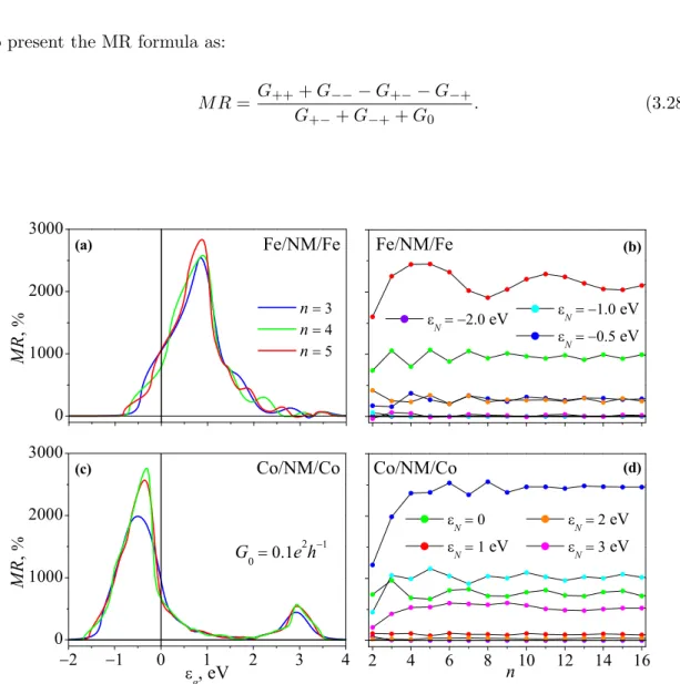
Chap. 2): (a) as a function of the on-site energy εg of the gate element for the same junction and various numbers of atomic planes in the gate element, ng= 3, ng= 4 and ng= 5. Compare the resonance peaks in the shallow band regime with those in the 1D case of Fig. 3.3; (b) in function of the number ng of spacer layers at fixed values of εg. Magnetoresistance of a Co/NM/Co junction (the parameters are given in the Chap. 2): (c) as a function of the on-site energy εg of the gate element for the same junction and various numbers of atomic planes in the gate element, ng = 3, ng = 4 and ng = 5; (d) in function of the number ng of spacer layers at fixed values of εg; . . . 42
3.7 Discrete electronic spectrum for n = 4 and t = −0.6 eV in the shallow band condition, εg = −1 eV. . . . 44
3.8 Schematic representation of the interface charge-energy, δ, created by a charge accumulation in the S/G and G/D interfaces, as a simplified description of the self-consistent behavior. . . . 45
function of mg with εg = 1 eV and δ varying from 0 to 0.4 eV. Effect of the interface charge energy on the MR for the same Co/NM/Co junction: (c) as a function of the εg, with mg = 4 and δ varying from 0 to 0.4 eV; (d) in function of mg with εg= −0.5 eV and δ varying from 0 to 0.4 eV. . . . 47
3.10 Schematic representation of an S-G-D junction, where each element is composed of 2D atomic planes with respective hopping parameters, and the voltage spatial distribution (by a staircase potential with equal steps E within the g element).. . . 48 3.11 (a) Discrete energy spectrum for a chain with n = 4 and t = 1/2 as a function
of y = E/(2t); (b) Eigenvector ψ(x, y) local amplitudes for the same chain. . . . . 51 3.12 Schematics of spin-dependent transport channels in P and AP regimes of the
junction (wide arrows indicate polarizations of the FM leads). For each channel with a certain absolute spin index Σ, the relative indices σ, σ0 are equal in P but different in AP. . . . 53 3.13 MR dependencies on the gate bias parameter εg for different numbers n of atomic
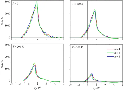
planes in the gate at different temperatures. . . . 55 3.14 (a) Electric field dependencies of MR for different numbers n of atomic planes in
the gate at room temperature; (b) Temperature dependencies of MR for the choices of gate bias εg adjusted to reaching SBR conditions at low and high temperatures. . 56
3.15 Transmission and reflection processes at given energy ε and the q-projected distributions of majority and minority spins on both sides of the barrier in the AP magnetic state. Light and dark shading indicates absolute spin orientations (up and down, respectively). . . . 58 3.16 Schematic picture of a magnetic junction: left ferromagnetic lead (source, S),
non-magnetic spacer (gate, G) and right ferronon-magnetic lead (drain, D). It is important to emphasize the discrete structure of the system, as that by n-atomic planes in the gate. . . . 64 3.17 Charge current, Ic, as a function of: (a) the on-site energy εg of the spacer; (b)
the angle θ; (c) the bias voltage V . . . . 74 3.18 The same dependencies as those presented for Ic, but for τk. . . . 75
3.19 Variation of τ⊥ with the same variables as for other transport currents. . . . 76
4.1 The energy diagram shows the on-site energy levels (dash-dot) for B- and G-spacers, the Fermi level (dashed) whose crossings with the continuous S- and D- dispersion curves (light grey for minority spins and grey for majority spins) define the spin-dependent wave numbers for incoming (qs,±), reflected (−qs,±) and transmitted (qd,±) parts of the Fermi state. Notice that the Fermi level generally does not match any of the discrete levels (solid) in the central B and G elements. . 80
indicates tunnel current. . . . 80 4.3 [(a),(c)] The TMR dependencies on εN (at different widths mI and mN) show
resonance enhancement, reaching ∼ 3000%; (b) TMR vs mI for various important εN values, different conduction regimes are explored; (d) TMR vs mN for the same εN values; . . . 84
4.4 Sketch of two types of double magnetic junctions: (a) FNINF and (b) FNFNF. Solid arrows are for polarizations of magnetic elements and dashed arrows for propagation of current. . . . 86 4.5 [(a),(c)] The TMR dependencies on εN (at different widths mI, mN) show
resonance enhancement, exceeding ∼ 6000%; (b) TMR vs mI for specific resonant εN values (at mN = 4); (d) TMR vs mN for the same εN values. . . . 88
4.6 [(a),(c)] The TMR dependencies on εN (at different widths mI, mN) show resonance enhancement, almost reaching ∼ 3000%; (b) TMR vs mN for various important εN values, different conduction regimes are explored; (d) TMR vs mF for the same εN values. . . . 89
4.7 Multiple-component system 0, ..., n + 1, the stripped view shows the atomically coherent internal structure of the layers and of the interfaces between them. . . . . 92 4.8 Magnetoresistance of a FNIFINF junction (with εI = 4.0 eV) as a function of
different parameters: (a) on-site energy, εN, for mN = 4, 5, 6 (shows a series of sharp peaks reaching ∼ 4000%); (b) TMR vs mI for εN = −1, −0.5, 0.5, 1, 2 eV; (c) TMR vs mF for the same εN values; (d) TMR vs mN for the same εN values. 99
4.9 MMagnetoresistance of a FINFNIF junction with the same definition of sets of parameters and panels as in Fig. 4.8 differs mainly from that case by the presence of single broad peak reaching ∼ 3000% in function of εN. . . . 100
4.10 Magnetoresistance of a FINFINF junction with the same definition of sets of parameters and panels as in Figs. 4.8 and 4.9. . . . 101 4.11 Magnetoresistance of a FIFNFIF junction with the same definition of sets of
parameters and panels as in Figs. 4.8, 4.9, and 4.10 shows two prominent peaks reaching ∼ 15000% in function of εN. . . . 102
5.1 Square lattice of metallic granules in the insulating matrix. . . . 104 5.2 Kinetic processes in a granular layer. . . . 106 5.3 CIP conduction geometry. . . . 107
2 exp −Ec/2kBT , and the curve 2 (dash-dotted line) to the high temperature asymp-totics ρ0≈ ρ∞− Ec/9kBT , converging to the limit ρ∞= 2/3 (dotted line). . . . . 109
5.5 The charge density σ in function of the carrier density ρ for different temperatures, corresponding to different thermal equilibrium values ρe. . . . 110
5.6 Kinetic process between nth granule and the metallic electrode in CA. . . . 113 5.7 Formation of local electrical field by charged granules and their images at the
surface of the metallic electrode (point a) and between the granules (point b). . . . 114 5.8 Relations between nth longitudinal (jx) and normal (jz) currents in CA. . . . 116
5.9 (a) Magnetization of Al2O3(3.0 nm)/[Co80Fe20(t)/Al2O3(4.0 nm) ]10 films with
t = 0.7 and 0.9 nm under H = 10 Oe in function of temperature. Insets show the Tb decay with the applied magnetic field. (b) Magnetization vs field cycles at different temperatures. . . . 121 5.10 (a) I-V characteristics for thickness t = 0.9 nm at different temperatures; Inset:
logarithmic representation of the low-voltage ohmic conductivity, g(T), divided by g(T = 100K) as a function of the inverse temperature. (b) Current vs temperature (with V = 5 V) for the same thickness.. . . 123 5.11 Conductivity as a function of T−1/2 for thicknesses t = 0.7, 0.9nm (fitted with the
Sheng et al. law [Sheng et al., 1973]). . . . 125 5.12 (a) Field dependence of room-temperature MR at different thicknesses t = 0.7, 0.9,
where the Inoue-Maekawa (IM) law for 3D granular films [Inoue and Maekawa, 1996] is used for fitting M R vs H; (b) IM fits at different temperatures for t = 0.7 nm (similar fits result for t = 0.9 nm). . . . 127 5.13 Comparison between the mean magnetic moments of the granules (in unities of
µB) calculated from the fits to the magnetoresistance, M R (•), and from the magnetization curves, M (H) (¥). . . . 129 5.14 Critical behavior at the SPM-SFM transition vs nominal thickness t of a granular
layer: (a) maximum MR ratio (M Rmax); (b) MR field sensitivity (dM R/dH) at
room temperature; (c) field Hi of maximum field sensitivity. Solid symbols stand for the previous data [Kakazei et al., 2003 and Sousa et al., 2001] and open symbols are for present measurements. Vertical lines delimit the ranges of SPM, SFM, and FM phases at this temperature. . . . 130 5.15 Maximum MR (H ≈ 9 kOe) temperature dependence for both the thicknesses:
t = 0.7 nm and t = 0.9 nm. . . . 131 5.16 Sudden change from a noisy MR behavior to a low noise behavior at T ∼ 220 K
for t = 0.9 nm. . . . 132 xxii
switches between a low and a high conductive state at around 10 V. (b) I-V characteristics of a device obtained after forming.(Notice the logarithmic vertical scale of these plots). . . . 134 5.18 Low-bias region of the final bistable current-voltage characteristics observed after
many ON/OFF cycles. . . . 136 5.19 (a) Step change in capacitance accompanying the resistive switching (f =1 kHz).
(b) Capacitance jumps between two discrete states occurring at a constant voltage. 137 5.20 Phenomenological model to explain the formation of a network of conducting paths
across the sample. . . . 139
6.1 An example of using the diagrammatic technics for calculation of orthogonal eigenstates. The set of diagrams defining the numerator of the orthogonalization coefficient O41 in Eq. (A4). . . . 149
6.2 Charge density and current distribution in CA region (regime I). . . . 153 6.3 Charge density in regime II. A fast decay is change to a slower exponential law,
after density dropping below the characteristic value ρ0. . . . 154
Introduction
1.1
Present Perspectives
Nowadays, we live in an information based society where knowledge has an extreme importance. In order to store the increasing amount of data, higher and higher storage densities are required. In some way, this fact is in a strict relation with modern devel-opment. Thus, ultra-high density storage technologies are a demanding research priority, receiving for that reason much attention from the scientific community. In this area, as well as in many others, the advent of nanotechnologies triggered plenty of new ideas and unexplored opportunities for theorists and experimentalists with both academic and industrial proposes. At the nanoscale, spintronics (spin-dependent electronics) has played a fundamental role, mainly in the fabrication of the vastly used hard-drive magnetic discs. In fact, the 2007 Physics Nobel Prize was attributed to Albert Fert and Peter Gr¨unberg for their contribution to this field. But definitely, this is not the end of the road for spintronics applications, and despite of the worldwide economical crisis, spintronics is still a growing field. For example, the designs of new spin-transfer torque random access memories (STT-RAM) [Krivorotov et al., 2005] and magnetic-domain wall motion based devices (racetrack memories) [Hayashi et al., 2008] are current research interests of leading companies such as IBM.
F Barrier Parallel state (a) Parallel state Antiparallel state Barrier Barrier F F eV eV MgO(001) MgO(001) (b) Coherent tunneling Incoherent tunneling MgO(001) Al-O Fe(001) Fe(001) Fe(001) Fe(001)
Figure 1.1: (a) Schematic illustration of the spin-dependent density of states (DOS) in a magnetic junction (red for majority spins and blue for minority ones) with parallel (upper panel) and anti-parallel (lower panel) magnetizations; (b) Schematic illustrations of incoherent electron tunneling through an amorphous barrier (upper panel) and coherent tunneling through a crystalline one (lower panel).
1.2
Magnetoresistance
The basic concept behind all these devices is the magnetoresistance (MR), the change of the electrical resistance (R) of a material when an external magnetic field (H) is applied, usually measured by the ratio:
M R(H) = R(H) − R(0)
R(0) × 100%, (1.1)
here R(H) is the resistance of the material subject to a magnetic field, H. This effect will obviously constitute the fundamental propriety studied in this thesis.
There is a variety of mechanisms responsible for such resistance variation. One example is the normal magnetoresistance, which is due to the effect of the Lorentz force on the electron’s trajectory (normally negligible in spintronic devices). Also, the anisotropic magnetoresistance (AMR) caused by spin-orbit coupling in transition ferromagnetic ma-terials (and their alloys) where the electrical resistance is a function of the angle between the magnetization and the direction of the current flow. Another example, is the colossal magnetoresistance (CMR) observed in doped manganate perovskites. In this kind of materials, the resistance changes by orders of magnitude as a result of a high magnetic field driven metal-insulator transition (near the Curie temperature). Furthermore, the most technologically relevant mechanisms are the giant magnetoresistance (GMR) and the tunnel magnetoresistance (TMR). They are related to a resistance variation of the MR devices promoted by a change of the relative angle between successive magnetiza-tions in magnetic multilayers, or by a variation of the angle between neighboring grains magnetizations in magnetic granular films. An illustration of the underlying spin-resolved density of states (DOS) causing MR in magnetic junctions is given in Fig. 1.1a. Normally, the resistance increases when the magnetizations are anti-aligned (anti-parallel, AP ) and decreases when they are aligned (parallel, P ), for that reason, the maximum GMR and TMR ratios are both given by:
M R = RAP − RP
RP × 100%, (1.2)
where RP (RAP) is the electrical resistance in the parallel (antiparallel) configuration. For
AP states can be used to store binary values: 0 and 1.
1.3
Overview
1.3.1 Magnetic Junctions
The first experiments in magnetic junctions were done by Tedrow and Meservey [Tedrow and Meservey, 1971] in Al/Al2O3/Ni junctions where spin-dependent tunneling
emerged. This work was followed by Julliere [Julliere, 1975], who observed an expressive TMR ratio of ∼ 14% at 4.2 K in a Fe/Ge-O/Co magnetic tunnel junction (MTJ). In this work, the famous Julliere formula was established: ∆R/R = 2P P0/(1+ P P0), where P, P0
are the spin polarizations of the conduction electrons of the two ferromagnetic metals. Nevertheless, this effect was not observable at room-temperature (RT). For that reason it received little attention until the works of Albert Fert [Baibich et al., 1988] and Peter G¨unberg groups [Binasch et al., 1989] on Fe/Cr superlattices and Fe/Cr/Fe simple junc-tions, respectively. These studies lead to the discovery of giant magnetoresistance effect. At that time, different theories were brought up to describe spin-dependent transport in these multilayers, the early ones were based on spin-dependent scattering effects (causing different relaxation times for different spin-channels) in the diffusive regime, [Bauer, 1992] and [Valet and Fert, 1993]. Only later it was shown that the spin-dependent scattering is not crucial for GMR. Instead, the ballistic spin-dependent reflection and localization controlled by interface potentials was proposed as the GMR mechanism. This model described successfully experimental data available at that moment, [Schep et al., 1995] and [Mathon et al., 1995].
Another breakthrough was achieved in the Meservey’s group by Moodera et al. with the discovery of large RT tunnel-magnetoresistance (TMR) in simple CoFe/Al2O3/Co
junctions [Moodera et al., 1995]. Inevitably, this finding attracted a great research effort, but even in the most optimized junctions TMR only reached a maximum of ∼ 70%, which is below the values required for magnetic random access memories (MRAM).
Nonetheless, two important theoretical works opened new perspectives, [Butler et al., 2001] and [Mathon and Umerski, 2001], describing coherent electronic magneto-conductance in perfect epitaxial Fe/MgO/Fe tunnel junctions. In such structures, MR ratio reached values above ∼ 1000% caused by the high spin polarized Fe ∆1 states, Fig.
1.1b. Three years later a suggestive MR of ∼ 200% was measured at RT in these type of junctions by groups of Yuasa [Yuasa et al., 2004] and Parkin [Parkin et al., 2004]. Since then, TMR values are continuously growing and for the moment, it reaches ∼ 604% at RT and ∼ 1140% at 5K [Ikeda et al., 2008].
1.3.2 Spin-Transfer Torque
On the other hand, only recently spin-transfer torque (STT) is receiving much attention from the spintronics community once it offers the possibility of current-controlled magnetization reversal and therewith a resistance switch. However, early works on current induced spin-transfer effects started already in the middle of 70ies by Berger. These preliminary attempts resulted in the subsequent observation of domain wall motion in thin ferromagnetic films under large currents (∼ 45 A) [Freitas and Berger, 1985]. Unfor-tunately, the high currents required for such motion did not attract much interest to the spin-transfer phenomena. In 1996, two crucial contributions to this field were presented by Slonczewski [Slonczewski, 1996] and Berger itself [Berger, 1996] predicting independently, that sufficiently high spin-polarized currents, flowing perpendicular to the plane in GMR multilayers, could generate a STT strong enough to switch the magnetization in one of the ferromagnetic leads. The experimental verification of spin-torque-driven excitations appeared three years later [Tsoi et al., 1998], and was followed by the observation of magnetization reversal [Myers et al., 1999]. Diverse works dealing with STT in GMR multilayers came afterwards. Although, development of high MR tunnel junctions (MgO based) shifted the researchers attention to STT phenomena in these devices. In fact, coherent tunneling can give rise to interesting effects such as anomalous bias dependence of the torque, as predicted by Theodonis and co-workers [Theodonis et al., 2006], and experimentally confirmed two years latter [Kubota et al., 2008].
1.3.3 Magnetic Granular Films
In parallel with the development of magnetic multilayered structures, as exposed above, magnetic granular films also involved an expressive research effort. This is due to the fact that these films have unique magnetic and transport properties, mainly controlled by the variation of concentration (x) or nominal thickness (t) of the magnetic materials.
magnetic grains in a host matrix (metallic or insulating). In particular, the studies by Gittleman et al. [Gittleman et al., 1972] on Ni/SiO2 films revealed some interesting
magnetic features. These were followed by the papers of Sheng and co-workers [Sheng et al., 1973], which clarified several transport aspects and established, besides the widely used conductivity thermal law: σ ∝ exp(−T−1/2). Two decades later Morawe and Zabel
[Morawe and Zabel, 1995] succeeded in preparing discontinuous metal/insulator multilayer (DMIM) systems which presented similar magnetic properties but rather improved MR performance. Yet, one year later, Inoue and Maekawa [Inoue and Maekawa, 1996] proposed a simple law to describe MR performance in cermet films. This important law is also valid for DMIM, but only at high temperatures.
There are various potential applications of this class of materials: high coercivity films for information storage, high permeability, high resistivity films for shielding and bit writing at high frequencies, and moderate MR elements for read heads and magnetic sen-sors. Further on, different granular ferromagnetic elements, such as Ni, Co, Fe, Co80Fe20, and Py, embedded into different insulating hosts, SiO2, TiO2, ZrO2, Al2O3, and HfO2,
have been combined and their properties are being extensively explored up to the present.
1.3.4 Resistive Switching
The resistive switching (RS) phenomena are characterized by large changes in the samples resistance, of the order of ∼ 103% resulting from application of an electrical field.
A proper voltage pulse can bring the device either into a high-resistance state (OFF) or into a low-resistance state (ON).
First experiments considering RS were performed by Hickmott in the beginnings of 1960s [Hickmott, 1962], studying capacitor-like metal-insulator-metal (MIM) structures, Al/Al2O3/Al. RS was thereafter reported in various MIM structures composed essentially
of binary metal oxides, such as SiO [Simmons and Verderber, 1967] and NiO [Gibbons and Beadle, 1964]. Already in the 1990s, complex transition metal oxides, like perovskite-type manganites and titanates, became the main object of interest for RS studies. This hap-pened thanks to the report of Asamitsu et al. [Asamitsu et al., 1997], on Pr0.7Ca0.3MnO3
(PCMO). This percussor results were followed by numerous studies exploring, principally, the driving mechanism of RS. Nevertheless, this mechanism is still elusive, preventing a large scale application of the effect. Thus, elucidation of the driving mechanism of RS is
currently a very important issue in the development of resistive random access memories (ReRAM).
1.4
Outline of the Thesis
The present thesis discusses two types of materials: magnetic multilayers and dis-continuous metal/insulator multilayers.
In the next chapter, Chap. 2, the theoretical methods and experimental techniques evolved in the realization of this work are explained. In Chap. 3, different aspects of tight-binding quantum-coherent transport in simple magnetic junctions are explored and further MR consequences are discussed. These are followed by a general treatment of magnetoconductance for arbitrary multilayered systems presented in Chap. 4. Then, in Chap. 5, discontinuous metal/insulator multilayer systems (in the low-concentration limit) are considered, where transport and magnetic properties are analyzed. Still in this chapter, electrical resistive switching phenomena discovered in these films are investigated. Finally, in the last chapter, conclusions and future perspectives are presented.
Theoretical Methods and
Experimental techniques
The present chapter describes the basic theoretical methods and experimental tech-niques used during the realization of this thesis. The next section, Sec. 5.2, concerns the theoretical part and the following, Sec. 5.3, deals with the experimental one.
2.1
Theoretical Methods
This section is divided as follows: in Subsec. 2.1.1 the basic aspects of electronic properties in solids are presented; in the next subsection, Subsec. 2.1.2, the fundamentals of the common tight-binding approximation (TB) are formulated; Subsec. 2.1.3 depicts the basis of electronic spin degree of freedom and presents its implications for the quantum description of electrons; finally, in order to explore electronic transport, in Subsec. 2.1.4, the important Landauer-B¨uttiker formalism is revised and several formulas, as well as some technical aspects of their numerical evaluation, are also described.
2.1.1 Electronic Properties of Solids
Describing electrons in a solid is a very complex many-body problem, in which the atomic Hamiltonian, that considers the interactions between electrons and the lattice mas-sive atomic nuclei, is perturbed by the presence of electron-electron interactions. Following the ideas of Landau, an independent electron approximation can be used regarding the effect of a potential U (r) in the one-electron quasi-particle Hamiltonian that includes all
these perturbations. Even neglecting the details of U (r), the periodicity of the crystal imposes that U (r + R) = U (r) for all Bravais lattice vectors R, and from this fact many important conclusions on the electronic properties of solids can be drawn. Typically, the effective potential (Fig. 2.1) approaches the individual atomic potential near the lattice ions and flats off in the mid-ion region. This potential profile led to the formulation of Bloch wave functions, a crucial aspect in the understanding of electronic properties of solids.
Figure 2.1: A typical crystalline periodic potential plotted along a line of ions (the rest of the crystal is not presented).
Bloch Wave Functions The three-dimensional (3D) single electron Schr¨ondiger equa-tion (SE) is then,
Hψ = µ −~2 2m∇ 2+ U (r) ¶ ψ = εψ, (2.1)
which is solvable in terms of periodic Bloch wave functions commonly referred to as Bloch electrons. This periodic wave functions obey a very important theorem:
Bloch’s Theorem The eigenstates ψ of an one-electron Hamiltonian, Eq. 2.1, where U (r + R) = U (r) for all R from a Bravais lattice, can be chosen as products of a plane wave with a function having a specific Bravais lattice periodicity as follows:
ψn,k(r) = eik·run,k(r), (2.2)
where ”n” is the band index and un,k(r + R) = un,k(r) for all R from a Bravais lattice.
This implies that: ψn,k(r + R) = eik·Rψ
n,k(r). Proofs of this fundamental theorem can
General Properties Obviously, this theorem has various consequences for the elec-tronic structure:
1. The Bloch wave vector k is not proportional to the electronic momentum p/~. 2. The Bloch wave vector can always be confined to the first Brillouin zone, since
exp(iK · R) = 1.
3. The band index n arises from different SE solutions for a given Bloch wave vector k.
4. For a given n, the eigenstates and eigenvalues are periodic functions of k on the reciprocal lattice: ψn,k+K(r) = ψn,k(r), εn,k+K = εn,k.
5. The mean velocity in an electron state labeled by (n, k) is given by: vn,k= ~−1∇ε n,k.
2.1.2 Tight-Binding Approximation
The tight-binding approximation (TB) is a very useful model to describe electronic properties in solids, since the atomic confinement does not exclude a weak overlap between wave functions of neighboring atoms, which generally causes a failure in the free-electron framework. The TB method was specially used to describe the energy bands of partially filled d-shells of transition metal atoms [Ashcroft and Mermin, 1976]. As an instructive exercise, the TB Hamiltonian can be derived from the SE describing electrons with effective mass m∗. So, considering a one-dimensional (1D) chain with the Hamiltonian:
H = − ~2 2m∗
d2
dx2 + U (x), (2.3)
a matrix formulation of this operator can be obtained from the quantity Hψ(x), where ψ(x) is any function of x. Now, it is possible to choose a discrete lattice with points at x = la (l ∈ Z) and write: [Hψ(x)]x=la= · − ~2 2m∗ d2ψ(x) dx2 ¸ x=la + Ulψl, (2.4)
here ψl ≈ ψ(x = la) and Ul ≈ U (x = la). Further on, it is necessary to consider the method of finite differences to deal with the derivative operators. Assuming a small, the
first derivative is approximated by: µ dψ dx ¶ x=(l+1 2)a ≈ ψl+1− ψl a , (2.5)
and the second derivative by: µ d2ψ dx2 ¶ x=(l+1 2)a ≈ 1 a "µ dψ dx ¶ x=(l+1 2)a − µ dψ dx ¶ x=(l−1 2)a # ≈ 1 a2 ³ ψl+1− 2ψl+ ψl−1 ´ . (2.6)
With this approximation, the SE becomes:
[Hψ(x)]x=la= (Ul+ 2t) ψl− tψl+1− tψl−1, (2.7)
with t = ~2/(2m∗a2). Thus the matrix representation of the 1D Hamiltonian operator for
electronic states on a linear chain is simply given by:
H = · · · −t 0 0 0 −t U−1+ 2t −t 0 0 0 −t U0+ 2t −t 0 0 0 −t U1+ 2t 0 0 0 0 −t · · · . (2.8)
Using the second quantization notation, this matrix representation can be written in a compact form: ˆ H =X l h εlˆa†lˆal− t ³
ˆa†lˆal+1+ ˆa†l+1ˆal ´i
, (2.9)
where εl= (Ul+ 2t) is the on-site energy, and ˆa†l(ˆal) is the Fermi creation (annihilation) operator on l-th site. The parameter t, which defines the hopping amplitude, is also known as the hopping integral, and it can be written, in a more general way, as
tij(R) =
Z
drψi∗(r)∆U (r)ψj(r − R),
depending on the Bravais lattice vector R. This integral involves the atomic wave functions in the ith, ψi(r), and jth, ψj(r − R), atomic levels of two atoms separated by a Bravais
vector R, and the perturbation term to the atomic (isolated) Hamiltonian, ∆U (r). This perturbation contains all the corrections required to produce the full periodic potential of a crystalline solid. The strength of the perturbation ∆U (r) obviously determines the hopping amplitude, in a way that stronger perturbations give rise to bigger overlap integrals. Nonetheless, ∆U (r) is typically weak, resulting in small hopping parameters. For instance, the d-bands of transition metals have values of tij(R) running from 0.2 eV to
1 eV, justifying the usage of this approximation when dealing with ferromagnetic metals. Considering overlap only between wave functions on the same atomic levels of nearest neighbors (subject to a specific lattice symmetry) reduces the general hopping integral tij(R) to t. As a matter of fact, this simplified form will be used throughout this work.
If, instead of an atomic chain, an atomic plane is studied, the Hamiltonian is expressed as: ˆ H =X n " εnˆa†nˆan− t X δ ³ ˆa†n+δˆan+ h.c. ´# , (2.10)
with the 2D lattice sites, n = (lx, ly)a, and the nearest neighbor vectors, δ. Further
generalization for a three-dimensional (3D) lattice is straightforward.
In practical calculations, planar-wave states (with a given planar momentum k) are frequently used to diagonalize the Hamiltonian by performing the Fourier transform: ˆak = N−1/2
P
nˆanexp(ik · n), with N being the number of lattice sites. With this
transformation, the Hamiltonian is simply given as ˆH =Pkεkˆa†kˆak, with the dispersion law, εk= ε0− t
P
δexp (ik · δ) (assuming that εn= ε0). As an illustrative example, a 2D
square lattice with δ = (±a, 0), (0, ±a) is considered. In this case, the energy dispersion law simplifies to:
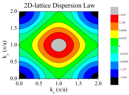
εk= ε0− 2t(cos kxa + cos kya), (2.11)
and its contour-plot is represented in Fig.2.2.
Single-Band Tight-Binding Parameters
For simplicity, the complex band structure of all the elements considered in this thesis will be simplified to a simple-cubic (sc) single-band tight-binding dispersion1. In particular,
the complex band structure of the ferromagnetic metals employed, iron (Fe) [Callaway
1A simple analytical model for two-band calculations is being developed, but it is out of the scope of
2D-lattice Dispersion Law k y ( / a ) k x ( /a)
Figure 2.2: Contour-plot of the dispersion law for a 2D square lattice with ε0= 0 and t = 1/2.
and Wang, 1977] and cobalt (Co) [Bagayoko et al., 1983], is simplified to a spin-dependent 3D dispersion law of the type:
εk,σ = εσ− 2t(cos kxa + cos kya + cos kza), (2.12)
here ε↑(↓)is the on-site energy of the majority (minority) band and t is the hopping integral amplitude, considered to be equal for both spin components. These laws roughly model the real d−bands (∆20, ∆5) that have an important contribution to the total electronic
density of states (DOS) in these materials.
So, to adjust the sc parameters to the real dispersions of Fig. 2.3, the Γ−H direction, kx = ky = 0 and kz ∈ {0, π/a}, is used and the resulting parameters are summarized in
Tab. 2.1. It is important to mention that besides the simplification of equal hopping amplitudes, the Stoner splitting ∆s = (ε↓ − ε↑)/2 is fixed for the entire band, even
though this assumption is not correct for the generality of the ferromagnetic materials, and definitely not true for Fe [Callaway and Wang, 1977].
F F E n e r g y ( e V ) (a) (b) F F
Figure 2.3: (a) Band dispersion of bcc Fe in the [0 0 1] direction, Γ − H; (b) Band dispersion of bcc Co in the same direction. (Reprinted from [Yuasa and Djayaprawira, 2007]). Thick red and blue lines respectively represent majority-spin and minority-spin band dispersions, Γ − H, used in this work for a sc lattice.
Element ε↑(eV) ε↓(eV) t(eV)
Fe 1.42 3.34 0.62
Co 0.57 2.10 0.62
Table 2.1: Single-band tight-binding parameters for Fe and Co (using the Fermi level reference, εF = 0).
2.1.3 Electron Spin
For spintronics (spin electronics) the electron spin represents the basic degree of freedom exploited in spin-dependent transport. In fact, this intriguing property is a fundamental result of relativistic treatment of quantum mechanics introduced by the famous Dirac equation. This formulation implies a profound modification in the quantum description of the electron properties. Historically, electron spin was discovered exper-imentally before the introduction of Dirac equation. Indeed, one of the most relevant experiments, among others, was performed in 1922 by Otto Stern and Walther Gerlach at the University of Frankfurt. They studied the deflection of a beam constituted by neutral and paramagnetic silver atoms subjected to a strongly non-uniform magnetic field, Fig. 2.4a. Contrarily to what was classically expected, only two main impact points were found, and for that reason only two magnetic moments could be measured, Fig. 2.4b. Motivated
by the results of different experiments, Wolfgang Pauli five years later developed a theory which allowed spin to be incorporated into non-relativistic quantum mechanics by adding four new postulates to its initial formulation. Since this thesis is restricted to the level of this phenomenological theory, some of its aspects are now presented. More details can be found in any text book, for example, in the standard quantum mechanical book [Cohen-Tannoudji et al., 1976]. (a) Inhomogeneous magnetic field Furnace Silver atoms What was actually observed Classical prediction (b)
Figure 2.4: (a) Schematic picture of basic elements of the Stern and Gerlach experiment. (b) Spin values for 1/2-fermions.
Postulates of the Pauli Theory
In addition to orbital variables, Pauli added the spin variables that satisfy the following postulates:
First Postulate: The spin operator s corresponds to an angular momentum, that means that its three components are the observables which satisfy the commutation relations: [sx, sy] = i~sz, and the other two formulas which are deduced by cyclic permutation of
the indices x, y, z.
Second Postulate: The spin operators act in a specific space, the spin state space Sσ. It
is spanned by the set of eigenstates |s, mi common to s2 and sz: s2|s, mi = s(s+1)~2|s, mi
and sz|s, mi = m~|s, mi and has finite dimension (2s + 1).
Third Postulate: The state space S of any considered particle is the tensor product of Sr (orbital space) and Sσ: S = Sr⊗ Sσ. Consequently, all the spin observables commute
with all orbital observables.
Fourth Postulate: The electron is a spin 1/2 particle (s = 1/2) and its intrinsic magnetic moment is given by: ms= 2(µB/~)s, where µB is the Bohr magnetron. For an
electron, the space Sσ is therefore 2D.
Properties of spin 1/2
The spin state space Sσ is 2D and an orthonormal system, {|+i, |−i}, of eigenkets,
common to s2 and s
z, is taken as a basis. These satisfy the equations:
s2|±i = 3 4~2|±i, sz|±i = ±12~|±i, h+|−i = 0, h+|+i = h−|−i = 1. The most general spin state is described by an arbitrary vector in Sσ:
|χi = c+|+i + c−|−i,
and any operator in this space can be represented by a 2 × 2 matrix, in the {|+i, , |−i} basis. In particular, the matrices for sx, sy, sz spin components are written in a simple
form, s = (~/2)σ, where σ represents the set of the three Pauli matrices:
σx = 0 1 1 0 , σy = 0 −i i 0 , σz = 1 0 0 −1 . (2.13)
These matrices have specific important properties:
σ2
x= σ2y = σ2z = 1,
Tr σx = Tr σy = Tr σz = 0,
Det σx = Det σy = Det σz= −1.
Furthermore, any 2 × 2 matrix can be written as a linear combination (with complex coefficients) of the three Pauli matrices and the identity. These four matrices form the Lee algebra for the SU (2) unitary group.
Spinor States
Any state |ψi from the S space can be expanded in the {|r, σi} basis as:
|ψi =X
σ
Z
dr|r, σihr, σ|ψi.
The vector |ψi can therefore be represented by the set of its components in the {|r, σi} basis, hr, σ|ψi = ψσ(r), which depend on three spacial coordinates x, y, z and on the spin
index σ = ±. Therefore, in order to characterize completely the state of an electron, it is necessary to specify two functions of the space variables: hr, +|ψi = ψ+(r) and hr, −|ψi =
ψ−(r). These two functions are often represented in the form of a two-component spinor,
which is written as:
[ψ](r) = ψ+(r) ψ−(r) (2.14)
with the respective adjoint: [ψ]†(r) =¡ψ∗
+(r), ψ−∗(r)
¢
. In this notation, the scalar product of two state vectors |ψi and |φi, is equal to:
hψ|φi = Z
dr[ψ]†(r)[φ](r) = Z
dr£ψ+∗(r)φ+(r) + ψ−∗(r)φ−(r)¤, (2.15)
and obviously the normalization of a vector |ψi is expressed by:
hψ|ψi = Z
dr£|ψ+(r)|2+ |ψ−(r)|2
¤ = 1.
Rotation of Spin States
It is known that the rotation operator Ru(α), in the state space, associated with the geometrical rotation Ru(α) by an angle α about the unit vector u, is expressed as Ru(α) =
exp[−(i/~)αJ.u], with J the total angular momentum. In the spin state space, Sσ, it reads R(s)u (θ) = exp[−(i/~)θs.u] = exp[−i(θ/2)σ.u]. For practical calculations it is rather
convenient to use its Taylor expansion, which can be simplified with the help of the Pauli matrices properties mentioned above. In this way, the rotation operator becomes:
Using this formula, is easy to express the rotation matrix in the {|+i, |−i} basis as:
Ru(1/2)(θ) =
cosθ2 − iuzsinθ2 (−iux− uy) sinθ2
(−iux+ uy) sinθ2 cosθ2 + iuzsinθ2
, (2.16)
where ux, uy, uz, are the Cartesian components of the vector u.
2.1.4 Landauer-B¨uttiker Formalism
The Landauer-B¨uttiker (LB) formalism [Landauer, 1957] and [B¨uttiker, 1988] de-scribing current passing through a finite mesoscopic region of non-interacting electrons has been largely used in various problems: universal conductance fluctuations, Aharonov-Bohm conductance oscillations, integer quantum Hall effect, and also commonly used in the spintronics studies [Bauer, 1992 and Schep et al., 1995].
In this low-dimensional systems the typical Drude formula for conductivity (the mean value over a large macroscopic number of modes) ceases to be valid. Thus, the main interest of LB formalism is the possibility to express the current in terms of the system microscopic properties: electron probability to be transmitted through it and distribution functions in the connected reservoirs. Another appealing reason to use this formalism is the fact that for coherent2 transport, the exclusion principle has no effect on the transmission
and it is possible to accurately describe the current flow in degenerate conductors in terms of single-particle transmission coefficient [S. Datta, 1995].
At zero temperature (ε = εF) and low voltages, the LB conductance formula is
simply written as a summation of the transmission probability, |T (εF, kk)|2, over the
available region K = K(εF) of transversal modes kk in the leads at the Fermi level (see
Fig. 2.5), multiplied by half quantum of conductance 2e2/h ∼ 1/(12.9kΩ):
G(εF) = e2 h
X
kk∈K
|T (εF, kk)|2. (2.17)
This results from the linear current I = I1+− I1− = I2+= G(εF)(µ1− µ2)/e, with µ1(µ2)
the chemical potential at the first (second) reservoir, Fig. 2.6a. Note that the pre-factor 2 due to spin degeneracy (appearing in the literature) is naturally not included since spin-dependent conduction rises up such degeneracy.
Figure 2.5: Schematic representation of both longitudinal q and transversal kk components of the total momentum k.
(a) (b)
Figure 2.6: (a) A conductor having a transmission probability of T is connected to two large contacts through two leads. Zero temperature is assumed such that the energy distributions of the incident electrons in the leads are step functions. Note that q is the longitudinal momentum.(b) A conductor is connected to two large contacts through two leads with energy distributions at non-zero temperatures.
![Figure 2.3: (a) Band dispersion of bcc Fe in the [0 0 1] direction, Γ − H ; (b) Band dispersion of bcc Co in the same direction](https://thumb-eu.123doks.com/thumbv2/123dok_br/15959180.1099002/40.892.286.693.108.418/figure-band-dispersion-bcc-direction-band-dispersion-direction.webp)