Viorel Dubceac
Bachelor in Micro and Nanotechnology Engineering
Influence of strain on Zinc Oxide nanoparticle
films on flexible substrates
Dissertação para obtenção do Grau de Mestre em
Engenharia de Micro e Nanotecnologias
Orientador: Dr. Martin Gall, Researcher, Fraunhofer
Institute for Ceramic Technologies and Systems Co-orientador: Prof. Dr. Luís Pereira, Associate Professor,
Faculdade de Ciências e Tecnologia da Universidade Nova de Lisboa
Júri
Presidente: Prof. Dr. Hugo Manuel Brito Águas
Arguente: Prof. Dr. Joana Maria Dória Vaz Pinto Morais Sarmento Vogal: Dr. André Clausner
Influence of strain on Zinc Oxide nanoparticle films on flexible substrates
Copyright © Viorel Dubceac, Faculdade de Ciências e Tecnologia, Universidade NOVA de Lisboa.
A Faculdade de Ciências e Tecnologia e a Universidade NOVA de Lisboa têm o direito, perpétuo e sem limites geográficos, de arquivar e publicar esta dissertação através de exemplares impressos reproduzidos em papel ou de forma digital, ou por qualquer outro meio conhecido ou que venha a ser inventado, e de a divulgar através de repositórios científicos e de admitir a sua cópia e distribuição com objetivos educacionais ou de inves-tigação, não comerciais, desde que seja dado crédito ao autor e editor.
Acknowledgements
First of all, I would like to thank Faculdade de Ciências e Tecnologia da Universidade Nova de Lisboa, and specially to Departamento de Ciências dos Materiais, for the oppor-tunity of this academic journey which is Micro and Nanotechnology Engineering. Here I had the opportunity to learn interesting subjects taught by successful people, something that was very inspiring for me. But I can’t say this journey was purely academic, I also met very good people.
Secondly, I must express my gratitude to Prof. Dr. Rodrigo Martins, Prof. Dr. Elvira Fortunato and Prof. Dr. Ehrenfried Zschech for conceiving me the opportunity to develop my master thesis at Fraunhofer IKTS, it was a privilege. Of course, nothing would be possible without Diana Gaspar’s work for making this journey as smooth as possible. Also, I would like to thank to my supervisors, Prof. Dr. Luís Pereira, Dr. Martin Gall and Dr. André Clausner, without their support I couldn’t finish this challenge.
I must also express my deepest gratitude to Daniela, Aránzazu and Simon for being my company during these five months and I can say that I will not forget some of the great moments that we shared together. As supervisors, Aránzazu and Hari were tireless assisting me with everything I needed and I am grateful for their help.
I would like also to express my gratitude to Yvonne, Dr. John, Christoph, Dr. Jürgen, Frieder and Dr. Rüdiger for providing all the time I needed of their help. In addition, I would like to thank to Sabrina and Marta and specially to Tiago for their availability to help.
As these five years weren’t just for learning, I’ve made some friends along the way. First of all, I would like to thank to Inês Martins for putting up with me for the last years and still being nice to me. Also, I want to that to Luís for being a good friend all these years and I hope we will for the next to come. My journey wouldn’t be so interesting if I hadn’t met a person like Tiago, aka Tiggus. Our main topics of discussion were always related with electronics and, without him, this subject would not be as interesting as it was. At last I want to thank to João Coroa for being the nicest guy I’ve ever known, to Ana Beaumont for always being in a good mood, to Marco, Shiv, Alex, Xana, João Crespo, Inês Caupers, João Fernandes, Joana Almeida, João Luís and David, you all made my experience better.
Of course, I could not finish without thanking to my godfathers Sofia Martins and José Rui. You have inspired and helped during these years.
And finally, I could not do everything what I’ve done without my family’s support, both during good times and not so good times.
Abstract
This work aims to study the effect of bending to the structural integrity and electrical
properties of ZnONanoparticles (NPs)films on a paper substrate. The films were printed by screen printing technique and afterwords the substrates were submitted to bending cycles. In order to evaluate the effect of bending cycles on the film’s morphology, the
first characterization technique was Scanning Electron Microscopy (SEM). It was pos-sible to verify that this stress led to crack formation. Other than imaging techniques, mechanical characterization was used, which was nanoindentation. This technique al-lowed to conclude that bending led to the decrease of Young’s Modulus (E) of the film which was provoked by the unpacking of theNPswhich composed the film. In addition, this unpacking was related with the increment of the film’s resistance. At the electrical characterization stage, two different compositions of ZnO inks were used and deposited on two different types of paper. The lowest resistance value achieved was with the ink
that contained water in it’s composition printed on an office paper substrate and had a
value of around 250 MΩ. On the other hand, the measured resistance increases about 40
times (to about 10 GΩ) when the ink contains toluene in it’s composition and is printed
on photographic paper. In order to determinate the influence of toluene to the paper’s surface, a study was performed where some pieces of photographic paper were immersed in toluene for different times. Furthermore, the samples were taken toFourier Transform Infrared Spectroscopy (FTIR)analysis where it was concluded that the paper’s surface is modified.
Keywords: Zinc Oxide, Nanoparticles, Flexible Electronics, Paper, Nanondentation, Bending.
Resumo
Este trabalho visa o estudo do efeito da flexão na integridade estrutural e propriedades eléctricas de filmes constituídos por nanopartículas de ZnO sobre papel. Para tal, os filmes começaram por ser impressos por serigrafia tendo depois os substratos sido submetidos a ciclos de flexão. Numa primeira fase, foi usada a técnica de microscopia eletrónica de varrimento de modo a avaliar o efeito do número de ciclos de flexão na morfologia dos filmes. Verificou-se que a tensão gerada nos leva à formação de fissuras. Para além de técnicas de microscopia, também foi usada uma técnica de caracterização mecânica, mais precisamente a nanoindentação. Esta técnica permitiu verificar que a flexão do substrato provoca uma diminuição do valor do módulo de Young dos filmes e que essa diminuição se deve ao desempacotamento das nanopartículas. Este desempacotamento está relacionado com o aumento da resistência eléctrica. Para a caracterização elétrica dos filmes foram usados quatro tipos de amostras impressas usando diferentes formulações da tinta de ZnO em diferentes tipos de papel. Os melhores resultados (resistência mais baixa) foram obtidos em filmes impressos sobre papel de escritório recorrendo a uma tinta que contém água na sua composição impressa, com uma resistência de 250 MΩ. Por outro lado, a
resistência medida aumenta quarenta vezes em filmes impressos em papel fotográfico recorrendo a tintas contendo tolueno na sua composição (cerca de 10 MΩ). De modo a
determinar a influência do tolueno na superfície do papel, foi feito um estudo em que vários amostras foram mergulhadas, durante diferentes períodos de tempo, em tolueno. Estas foram posteriormente analisadas porFTIRonde se concluiu que a superfície do papel é modificada.
Palavras-chave: Óxido de Zinco, Nanopartículas, Eletrónica flexível, Papel, Nanoindeta-ção, Flexão
Contents
List of Figures xv
List of Tables xvii
Glossary xix
Acronyms xxi
1 Introduction 5
1.1 Flexible electronics and paper . . . 5
1.2 Zinc Oxide Nanoparticles for flexible electronics . . . 6
1.3 Electron Microscopy. . . 7
1.4 Mechanical Properties of Thin Films and Nanoindentation. . . 9
2 Materials and Methods 11 2.1 Printing process and ink formulation . . . 11
2.2 Three-point bending for stress induction . . . 11
2.3 SEM sample preparation . . . 12
2.4 Nanoindentation sample preparation . . . 12
2.5 Sample preparation for electric characterization . . . 12
2.6 Sample preparation for 3D profilometry . . . 12
3 Results and Discussion 15 3.1 Study of the film's surface . . . 15
3.1.1 Electron microscopy . . . 15
3.1.2 Film adhesion and crack propagation. . . 19
3.1.3 Printing mesh . . . 21
3.1.4 Profilometry . . . 21
3.2 Mechanical characterization . . . 23
3.3 Electrical characterization . . . 26
3.4 Study of the influence of solvent on substrate's surface . . . 27
3.4.1 SEM and EDS analysis . . . 28
C O N T E N T S
3.4.3 Profilometry . . . 29
4 Conclusions and Future Perspectives 31 4.1 Conclusions . . . 31
4.2 Future perspectives . . . 32
Bibliography 33 A Bending machine 39 B Nanoindentation 41 B.1 Berkovich indenter . . . 41
B.2 Oliver and Pharr method . . . 41
B.3 Load function . . . 42
B.4 System calibration . . . 44
C Photographic paper (FS3) properties 45
D ZnO NPs on office paper substrate 47
E SEM results for different immersion times in toluene 49
List of Figures
1.1 Some examples of flexible electronics. . . 6
3.1 SEM results with a 447 times magnification with the HE-SE detector. . . 16
3.2 SEM results with a 692 times magnification with the HE-SE detector. . . 17
3.3 SEM results with a 692 times magnification with the EsB detector. . . 17
3.4 SEM results with a 1920 times magnification with the HE-SE detector. . . 18
3.5 SEM results with a 1920 times magnification with the EsB detector. . . 19
3.6 SEM results with a 2100 times magnification with the HE-SE detector. . . 20
3.7 SEM results with a 2100 times magnification with the EsB detector. . . 20
3.8 Cross section of sample with 1000 bending cycles. . . 21
3.9 Printing mesh. . . 22
3.10 3D perfilometry results. . . 22
3.11 Regions where nanoindentation was performed.. . . 23
3.12 Young’s modulus and Hardness film’s results. . . 25
3.13 Young’s modulus and hardness substrate’s results. . . 26
3.14 Electric characterization results. . . 27
3.15 SEM and EDS results of the substrate. . . 28
3.16 FTIR spectrum of the FS3 substrate.. . . 29
3.17 FTIR spectra for immersed substrate. . . 30
3.18 Roughness results for the tolene immersion time. . . 30
A.1 Bending machine. . . 40
B.1 Berkovich indenter geometry. . . 41
B.2 Pile-up and sink-in effects. . . 43
B.3 Load function. . . 43
B.4 Calibration on the nanoindentation system. . . 44
C.1 Layered system of the substrate. . . 45
D.1 SEM result of the ZnO film on office paper substrate. . . 47
E.1 SEM of the substrate’s surface. . . 49
List of Tables
2.1 Three point bending machine parameters. . . 11
3.1 FTIR peaks.. . . 29
C.1 Substrate properties. . . 45
Glossary
β Geometry correction factor. υ Poisson’s ratio.
ε Intercept factor.
υi Poisson’s ration of the indenter.
Ac Contact area.
E Young’s modulus, also known as elastic modulus. Ei Elastic modulus of the indenter.
Er Reduced Elastic modulus. H Hardness.
L Distance between supporting pins. Pmax Maximum load.
S Contact Stiffness.
Tg Glass transition temperature. Z Atomic number.
hc Penetration depth.
hf Penetration depth left by indenter after the experiment.
hmax Total indentation depth measured from specimen free surface.
Acronyms
1D One Dimension.
2D Two Dimensions.
3D Three Dimensions.
ATR Attenuated total reflection.
BSE Backscattered electron.
CEMOP Center of Excellence in Microelectronics Optoelectronics and Processes.
DSI Depth-sensing indentation.
EDS Energy Dispersive X-Ray Spectroscopy.
EsB Energy selective Backscattered.
FIB Focused Ion Beam.
FTIR Fourier Transform Infrared Spectroscopy.
HE-SE High efficiency secondary electron.
IIT Instrumented indentation testing.
LPG Liquefied petroleum gas.
NPs Nanoparticles.
NW Nanowire.
PE Polyethylene.
PEN Polyethylene naphthalate.
PET Polyethylene terephthalate.
PI Polyimide.
PP Polypropylene.
AC R O N Y M S
PTFE Polytetraflouroethylene.
R2R Roll-to-Roll.
RFID Radio-frequency identification.
RMS Root mean square.
SE Secondary electron.
SEM Scanning Electron Microscopy.
TFT Thin Film Transistor.
UV Ultraviolet.
Motivation
Nowadays, flexible electronics has received an increasing attention for its applications such as flexible displays, biomedical devices andRadio-frequency identification (RFID)
tags. Coupled with the flexible electronics technology comes low cost production pro-cesses, which, besides flexibility, is another advantage over the silicon based technology.
With paper being the most common biopolymer on Earth, it becomes a strong candi-date to be used as a substrate in flexible electronic applications since it shares the isolating properties of most common polymer substrates such asPolyethylene terephthalate (PET)
andPolyimide (PI). Besides being common, paper is also a recyclable material which opens the possibility for a more environmentally friendly technology.
With the development of flexible electronic technology, it becomes important to de-velop knowledge about the influence of stress on the active layers. To study the influence of bending and stress, is necessary to use additional characterization techniques, such as
SEMimaging techniques and mechanical characterization, besides resistance measure-ments since this technique does not provide the entire picture of what stress is causing to the material.
Objectives
The objective of the work developed with this thesis is to determine how stress induced to the ZnO film affects its properties and the topography of screen printed films. In a first characterization step,SEMimaging will be used to image how is the film’s topography after printing and after bending, in the hope of observing some progress of crack forma-tion (or other type of structures) with the increment of bending cycles. From theSEM
results, some regions will be chosen to perform nanoindentation experiments to check if there are any changes in mechanical properties of the film with bending and, if so, to see if there is any relation between bending cycles and mechanical properties.
Since the ZnO material will be used in flexible electronic circuits, it is also important to perform electrical characterization of the printed films. If the stress induced to the film (bending cycles) has any influence on the electrical properties, will be important to prove how. Besides stress, at this stage, the influence of the substrate will be studied with two different papers (office paper and photographic paper). In addition, two types of inks
will be printed (one with toluene in its formulation and one with water) to see if there is any influence as well.
As toluene is a well knows solvent, it is important to see how it affects the substrate
when present in the ink formulation. For that,SEM, FTIRandThree Dimensions (3D)
profilometry will be used.
CHAPTER
1
Introduction
1.1 Flexible electronics and paper
Traditional electronics are generally built on thick inflexible substrates. Instead, flexible electronics – built on organic substrates (like plastic or paper) or metallic foil – can be folded, wrapped, rolled, and twisted with negligible effect on its electronic function.
Flexible electronics is usually composed by a layer of passive substrate topped with a second layer of active electronic components. In some applications, additional layers may be used for encapsulation or packaging [1]. Flexibility can mean different properties to
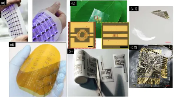
manufacturers and users. As a mechanical characteristic, it is conveniently classified in the three categories: bendable or rollable; permanently shaped and elastically stretchable, where some examples are presented on Figure1.1[2].
In flexible electronics, all components must comply with bending to some degree without losing their function. Two basic approaches have been employed to make flex-ible electronics: transfer and bonding of completed circuits to a flexflex-ible substrate and fabrication of the circuits directly on the flexible substrate. In addition to flexibility, such substrates should be relatively inexpensive, mechanically/thermally robust and resistant to creep, thermally conductive, but electrically passive. The glass transition temperature (Tg) of the substrate (if the substrate is a plastic material) must be compatible with the maximum fabrication process temperature. Mechanically, the substrate should have a high elastic modulus to make it stiff, and a hard surface support the device layers under
impact. Surface roughness is also an important parameter and it should be free from structural defects like pits and pinholes since the thinner the device films, the more sensi-tive their electrical function is to surface roughness. Polymer substrates such as Kapton®
polyimide, Polytetraflouroethylene (PTFE), PET, and Polyethylene naphthalate (PEN)
have been used for various applications [1,2,8].
C H A P T E R 1 . I N T R O D U C T I O N (a) (b) (c.1) (c.2) (d) (e)
Figure 1.1: Here are presented some developments on the flexible electronics field. Ex-ample (a) represents some advances on stretchable (and flexible) electronics for health monitoring, on (b) is presented a high-performance circuit on a flexible and biodegrad-able cellulose nanofibril paper substrate, on (c) is presented an ultrathin plastic electronic foil (lighter than a feather), on (d) is presented a high-speed analogue and digital circuit operating at low voltage and finally, (e) presents low cost methods for fabricating flexible electronic circuits on paper. Adapted from [3–7].
related with the use of biopolymers such as paper for electronic applications (like pa-per electronics), mainly driven by its low cost (≈0.1 centdm−2), much cheaper than the
cheapest polymer based substrate, which isPET(≈2 centdm−2) andPI(≈30 centdm−2),
lightness, flexibility and environmentally friendly since it is recyclable and made of re-newable raw materials [9–12]. While paper is mainly used for packaging and for display-ing and stordisplay-ing information, paper has also recently been considered as a potential sub-strate for low-cost flexible electronics [13]. The typical requirement of very smooth and non-absorbing substrates for printed electronic components is an important issue when considering the use of paper as a substrate. In a converting process different functional
coating can be applied to the paper surface such asPolyethylene (PE),Polypropylene (PP),
PET, wax, or aluminium. The cost of a plastic-coated paper might, however, become too large (or a too substantial part) in situations when the electronics are truly low cost and robust,i.e., consistingRoll-to-Roll (R2R)printed low-cost materials and do not require
encapsulation. Furthermore, the recyclability or biodegrability might be a very essential constraint in some cases [12].
1.2 Zinc Oxide Nanoparticles for flexible electronics
ZnO is an excellent intrinsically n-type inorganic semiconductor with wurtzite structure. It naturally appears as an option in printed and flexible electronics due to its properties. It
1 . 3 . E L E C T R O N M I C R O S C O P Y
became one of the most important candidate in optoelectronics due to its high and direct band gap, around 3.4 eV (i.e. in the near-Ultraviolet (UV)) at room temperature [14–19].
It has been demonstrated that ZnO can be used inUVphotodetectors as aNanowire (NW)
film [20,21]. Furthermore, a very simple ZnO – paperUVsensor outperformed in terms of responsivity and response time of a similar sensor where the substrate was glass or a thin film [22–24].
Another characteristic of this material is its high excitation binding energy (60 meV) at room temperature thus, it can act as an efficient piezoelectric material [17, 25, 26].
Being a biologically safe piezoelectric semiconductor occurring in a wide range of One Dimension (1D)andTwo Dimensions (2D)forms of nanostructures, this material can be used in areas that require flexible power sources as nanogenerators. It has the potential to be implanted and convert biomechanical energy in the human body, such as blood flow, heartbeat or muscle stretching, into electricity to power implanted devices [27–31].
ZnO nanostructures can be useful in photovoltaics due to high surface to volume ratio, low reflectivity that enhances light absorption and finally, fast electron transport along the crystalline1Dnanostructures that improves charge collection efficiency [27]. Another advantage of ZnONPsis its gas sensing properties. As gas sensing is a surface phenomenon and henceNPscan improve the performance of gas sensor due to their large surface area [32]. It has been demonstrated to work with CO, NO2, Ethanol andLiquefied
petroleum gas (LPG). The results were promising since it was achieved a sensitivity below 100 ppm (for NO2) but there is still room for progress since the response time
and working temperature were still quite high in the range of hundreds of ◦C for the
temperature and in the range of tens of min for the response time [32,33].
Overall, ZnO is a strong candidate for commercial purposes since it’s relatively abun-dant, chemically stable and transparent in the visible region when compared with organic n-type semiconductors. Furthermore, ZnO has a simple and a wide range of crystal-growth technologies [15,27,34].
In a real world application these flexible systems will be submitted to a lot of bending. In an attempt to create these bending conditions in a controlled manner, the films will be submitted to bending with a bending machine which is presented on AppendixA. The bending cycles will provoke crack formation (among other things) which will be imaged bySEMand mechanically characterized by nanoindentation and electrically character-ized. The mechanical characterization method will allow to determine if the films are affected at the nanoscale,NPsdislocation and other effects.
1.3 Electron Microscopy
An electron microscope uses an electron beam to produce a magnified image of the sample. As the electrons penetrate the surface, several interactions can occur, such as absorption of electrons by the sample, reflection of primary (backscattered) electrons, emission of secondary electrons and emission of electromagnetic radiation. SEMrelies
C H A P T E R 1 . I N T R O D U C T I O N
on these interactions to provide high resolution images of the surface of a sample, being possible to analyse features in the nanometer scale. The image in anSEMis produced by scanning the sample with a focused electron beam (in vacuum) and detecting the secondary and/or backscattered electrons [35,36]. The pressure in the specimen chamber is typically around 10−4Pa, allowing the beam electrons to travel from the cathode to the
specimen with little interaction (increasing the mean free path of the electrons) with the residual gas molecules [37].
Secondary electrons (SEs)andBackscattered electrons (BSEs)are separated according to their energies and, they are produced by different mechanisms [36]. When a high-energy primary electron interacts with an atom, it undergoes either inelastic scattering with atomic electrons or elastic scattering with the atomic nucleus. In an inelastic collision with an electron, some energy is transferred to the other electron. If the energy transfer is high enough,i.e., its energy exceeds the material’s work function, the electron will leave
the material and can be detected. On the other hand, if the energy is not high enough, the electron won’t be detected. If the energy of the emitted electron is less than 50 eV, by convention, it is referred to as aSE. Most of the emittedSEsare produced within the first few nm of the surface, this is the reason why they will provide topographical information of the material. SEs produced much deeper in the material suffer additional inelastic collisions, which lower their energy, and trap them in the interior of the solid [36]. These electrons are attracted and collected by the detector even if they leave the sample in a direction away from the detector since the detector is positively charged to increase the number of detected electrons [35].
Higher energy electrons are primary electrons that have been scattered elastically,i.e.,
without loss of kinetic energy, by the nucleus of an atom. BSEsare the electrons that exit the specimen with an energy greater than 50 eV. However mostBSEshave energies comparable to the energy of the primary beam [36]. The contrast in anSEMdepends on many factors. For a flat, uniform sample the image shows no contrast. If, however, the sample is formed by materials containing different elements, and therefore different
atomic numbers, a contrast is observed if the signal is obtained fromBSEs, because the backscattering coefficient increases with the atomic numberZ. There is a built in contrast
caused by elemental differences which means if two materials (high-Z and low-Z) are side by side on anSEMsystem, the high-Zmaterial should be brighter because there is
moreBSEsemission [35,36].
When compared with optical microscopy, SEM has the disadvantage to work with conductive samples but it has been shown low voltage techniques by Garitagoitia Cid
et al. [38]. On the other hand, much larger magnifications are possible since electron
wavelengths are much smaller than photon wavelengths and the depth of field is much higher [35].
1 . 4 . M E C H A N I CA L P R O P E R T I E S O F T H I N F I L M S A N D N A N O I N D E N TAT I O N
1.4 Mechanical Properties of Thin Films and Nanoindentation
The interest on mechanical characterization of thin film systems and small volume mate-rials has been increasing in the last decades. The characterization method usually used is depth-sensing indentation tests using spherical or pyramidal indenters. The tests are performed with the intent of extracting values of elastic modulus,E, and hardness,H, of
the specimen material from experimental readings. The depth of penetration is in the order of nanometers, hence the term “nanoindentation” [39].
In conventional indentation tests the contact area is determined from the direct mea-surement of the dimensions of the residual impression left in the specimen surface upon the removal of load. Meanwhile, in nanoindentation tests, the size of the residual im-pression left in the specimen is in the order of microns, which is too small to be mea-sured directly. So, to overcome this obstacle, it is meamea-sured the depth of penetration into the specimen during the test and, combining this with the known geometry of the indenter, it is possible to do an indirect measurement of the area of contact. For this rea-son, nanoindentation testing can be considered a special case of the more general terms:
Depth-sensing indentation (DSI)orInstrumented indentation testing (IIT)[39].
Nanoindentation is an instrumented indentation method that consists essentially of touching the material of interest whose mechanical properties, such as elastic modulus and hardness, are unknown with an indenter whose mechanical properties and geometry are known. In nanoindentation, an indenter tip is driven into the material to be tested by applying an increased normal load. Upon reaching the maximum value, the normal load is reduced until partial or complete relaxation. The position of the indenter relative to the sample surface is precisely monitored and a load – displacement curve is obtained [39,40].
Nanoindentation’s main advantage is that no special requirements regarding the spec-imen shape or preparation are needed for the Young’s modulus evaluation. Also, indenta-tion experiments are simple, cost effective and reproducible when compared with tensile (or compression) tests. These tests can be automated and on one sample can be performed hundreds of experiments. Moreover, the ability to test at very small penetration depths allows testing of thin films or regions of the sample’s microstructure independently. For instance, Young’s moduli measured on a homogeneous material result in a standard devi-ation of around 1 % at 10 nm penetrdevi-ation depth [41–43].
As a disadvantage, a flat surface is a precondition for high spatial resolution in nanoin-dentation. This condition is critical for low indentation depths, when the penetration depth is similar to the local roughness of the sample. So, for very thin films, where low indentation depths are needed, strong scatter in the data of hardness tests can appear [41,
42].
When the indenter penetrates the material not only deforms the film, but also the substrate thus, the mechanical properties for the film must be determined by suitable processing of data. This creates a restrain on the penetration depth of thin films so, the
C H A P T E R 1 . I N T R O D U C T I O N
commonly used rule of thumb is to limit the indentation depth to less than 10 % of the film thickness [39,42–45].
In case of soft films on hard substrates, the problem of pile-up (see Figure B.2in AppendixB) also must be considered. The Oliver and Pharr method (which is the most common method used for nanoindentation data and is presented on AppendixB) does not take the pile-up area into account in the area calculation, leading to inaccurately high values of hardness [46,47].
CHAPTER
2
Materials and Methods
2.1 Printing process and ink formulation
The films were deposited by screen printing technique using a mesh with holes around 77 µm. The projected thickness was around 20 µm but, since a manual process was used, it is very difficult to ensure that the thickness is consistent through all samples. The sizes
of the printed patterns were 1.5 cm by 3 cm. For this work, two inks were used, one that
used water (Z40C3) and other that used toluene (Z40T80). These inks were also printed on two different substrates – photographic paper FS3 and regular office paper – obtaining
four different sample systems (A Z40C3/OP, B Z40C3/FS3, C Z40T80/OP and D
-Z40T80/FS3). The main focus of this work will be sample D but, on Section3.3will be presented results regarding all four samples.
2.2 Three-point bending for stress induction
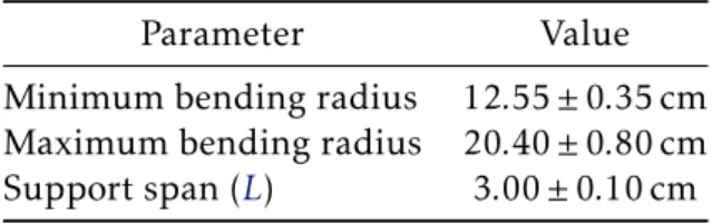
In order to induce some stress into the film in a controlled and reproducible manner, a three-point bending machine was used. This machine (see AppendixA) was built by
Center of Excellence in Microelectronics Optoelectronics and Processes (CEMOP)using a
3Dprinter. The bending was performed on three samples where one was bent 100 times, other 500 times and other 1000 times.
Table 2.1: Three point bending machine parameters. Parameter Value
Minimum bending radius 12.55±0.35 cm
Maximum bending radius 20.40±0.80 cm
Support span (L) 3.00±0.10 cm
C H A P T E R 2 . M AT E R I A L S A N D M E T H O D S
2.3 SEM sample preparation
For simpleSEMimages the sample was simply cut and taken into theSEMchamber. The majority of theSEMimages were taken with aCarl Zeiss GEMINI 500. When aFocused Ion Beam (FIB)cut was needed the sample was covered with a 5 nm thick gold layer to make the surface more conductive so it could drain charges more easily. TheFIBcuts were performed onFEI Helios NanoLabTM660andCarl Zeiss SEM/FIB NVision 40.
2.4 Nanoindentation sample preparation
The nanoindentation experiments were performed by aHysitron TI 950 Triboindenter®
tool on 3 different regions with a Berkovich indenter. For each region, the indents were performed with a maximum load,Pmax, of 1000 µN, 2500 µN and 5000 µN (see FigureB.3
on Appendix B). For eachPmax 20 indents were performed to have a statistical result.
Loading time, which is the time the indenter takes to reach Pmax, was 5 s, creep time,
which is the time the maximum load is applied, was 10 s, and unloading time was 5 s again (see FigureB.3on AppendixB). It is important that the sample stays flat without any air gaps between the surface that supports the sample and the sample itself. If not, it will produce false (and lower) values of mechanical properties like Young’s Modulus and Hardness on those regions. In order to avoid this phenomenon it was used a glue to fixate the samples.
2.5 Sample preparation for electric characterization
To be able to perform electrical characterization to the films, it is needed to create a contact layer between the film and the probes. Thus, an aluminium layer with a thickness of 120 nm was deposited on top of the ZnO. The contacts were deposited by e-beam assisted thermal evaporation using shadow masks and they were about 1 mm apart and were 4 mm long. The electrical characterization was performed with on a HP 4155C + Cascade M150 system.
2.6 Sample preparation for 3D profilometry
The 3D profilometry was performed on a Ambios XP-Plus 200 Stylus tool where the perfilometer would scan the surface in one direction for 0.5 mm. After one scan, the stylus would move 3 µm in the perpendicular direction of the scan. That process is repeated 165 times resulting in a scanned area of roughly 0.5 mm by 0.5 mm. The scan
was performed at a speed of 0.1 mms−1. With this technique it is also important for the
sample to stay as flat as possible since bent surfaces will decrease the tool’s resolution. Of course, when working with paper (flexible and conformable material) the surface will
2 . 6 . SA M P L E P R E PA R AT I O N F O R 3 D P R O F I L O M E T RY
always be curved (especially after the bending cycles were performed on the sample) and this effect was minimised by using duct tape.
CHAPTER
3
Results and Discussion
3.1 Study of the film's surface
3.1.1 Electron microscopy
In this section, the SEM images taken with both detectors, High efficiency secondary electron (HE-SE)detector andEnergy selective Backscattered (EsB)electron detectorand were taken with an acceleration voltage of 1 kV and a working distance of 2.9 mm. The images produced with the EsB electron detector had the grid voltage set to 500 V. As said previously, the samples analysed by this technique is sample D which is a toluene containing ink (Z40T80) layered on photographic paper (FS3).
On Figure3.1is presented an overview of the morphology of each sample using the
HE-SEdetector. From this general overview is possible to see the progress of the film’s topography with the increment of bending cycles. It is also noticeable the rounding effect
on Figure 3.1c around the valleys. These structures – valleys – appear to be regularly spaced with similar shape and area.
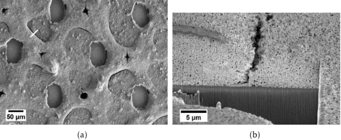
On Figure 3.2 are presented images for the same samples on the same region as Figure3.1, but with a magnification of 692 times. Here it is possible to see with greater detail the structures created on the film’s surface. The easiest thing to notice is the valleys’ presence. They are present on all samples and appear to be equally spaced which implies that these structures are created during the printing process and not due to bending cycles. These valleys have an area of around 3000 µm2 (on Figure3.2d). Between the
valleys, there are some dark dots – holes – that are regularly spaced and shaped, and they appear on Figure 3.2a, which implies that they were not created during bending. Although its origin is uncertain, i.e., it is not clear how these holes are created, there
might be a cause for the creation of the valleys, which will be discussed latter.
C H A P T E R 3 . R E S U LT S A N D D I S C U S S I O N
(a)
(c)
(b)
(d)
Figure 3.1: SEMimages taken with theHE-SEdetector with a 447 times magnification. Sample (a) corresponds to 0 bending cycles, (b) corresponds to 100 bending cycles, (c) corresponds to 500 bending cycles and (d) corresponds to 1000 bending cycles.
appear to be randomly shaped. On Figure 3.2d it is possible to see one hole and three cracks and it is clear the difference between them, the cracks have a star like shape while,
holes are round.
From Figure3.3it is possible to see with more detail cracks formed around the valleys, and other cracks formed between them. The bottom of the valleys expose the substrate’s surface. That is a conclusion that can be made due to the fact that the EsBdetector is sensitive to atomic weight differences since it detects theBSEs, and the substrate appears
darker in the image, so it can be distinguished from the film. Another conclusion that can be reached from these results is that the substrate’s surface composition is made with lighter atoms than the film, since is a darker region.
Comparing the valleys from Figures3.3a and3.3d it is clear that the valleys on unbent samples expose less area of substrate than the sample with 1000 bending cycles. It is clear that this was caused by the bending – stress – imposed to the film which made theNPs, that didn’t belong to bigger agglomerates, to peel offthe substrate, thus exposing more substrate. In addition, there is a clear increase in cracks on the film as the bending cycles increase.
An artifact present on all images taken with theEsBelectron detector is the rounded brighter region. This region is theSEMbeam and the honeycomb structure is formed due to the presence of the detector’s grid.
On Figure3.4is presented the valleys’ evolution with bending cycles when analysed with the HE-SEdetector. These structures were created during printing by the mesh.
3 . 1 . S T U DY O F T H E F I L M ' S S U R FAC E
(a)
(c)
(b)
(d)
Figure 3.2: SEMimages taken with theHE-SEdetector with a 692 times magnification. Sample (a) corresponds to 0 bending cycles, (b) corresponds to 100 bending cycles, (c) corresponds to 500 bending cycles and (d) corresponds to 1000 bending cycles.
(a)
(c)
(b)
(d)
Figure 3.3: SEMimages taken with theEsBelectron detector with a 692 times magnifica-tion. Sample (a) corresponds to 0 bending cycles, (b) corresponds to 100 bending cycles, (c) corresponds to 500 bending cycles and (d) corresponds to 1000 bending cycles.
C H A P T E R 3 . R E S U LT S A N D D I S C U S S I O N
They were created either by removing material on those regions with the mesh or because the mesh didn’t allow any deposition on those regions, leaving the valleys presented on Figures3.1,3.2and3.4. These structures limit the cross-section area for which increases the film’s electrical resistivity.
The structure of valleys is not random since almost all valleys have an elliptical shape on the bottom where the substrate is (almost always) exposed (region 1), a flat region right by it (region 2) and, finally, a thicker layer of material around it (region 3). On Figure 3.11on Page23, Section3.2, these regions are specified. There is a preferential formation of cracks between the two latter regions mentioned previously. These types of cracks might be formed during compression bending because, assuming that region 2 is less compliant than region 3 because theNPs are more segregated, they force the
NPsfrom region 3 to go up, as it happens with converging tectonic plates. This is just an hypothesis and is in accordance with the nanoindentation results that will be presented latter on.
(a)
(c)
(b)
(d)
Figure 3.4:SEMimages taken with theHE-SEdetector with a 1920 times magnification. Sample (a) corresponds to 0 bending cycles, (b) corresponds to 100 bending cycles, (c) corresponds to 500 bending cycles and (d) corresponds to 1000 bending cycles.
On Figure3.5are presented the same exact valleys but with theEsBelectron detector. The substrate is exposed and this is confirmed by the difference of grey level which indicates different material composition.
The cracks formed between valleys due to bending can be seen in more detail in Figure 3.6. On Figure 3.6a is presented an overview of the valleys without any cracks, which is something expected since that sample didn’t suffer any bending cycles. Since
3 . 1 . S T U DY O F T H E F I L M ' S S U R FAC E
(a)
(c)
(b)
(d)
Figure 3.5:SEMimages taken with theEsBelectron detector with a 1920 times magnifica-tion. Sample (a) corresponds to 0 bending cycles, (b) corresponds to 100 bending cycles, (c) corresponds to 500 bending cycles and (d) corresponds to 1000 bending cycles.
from stress (bending). The region where these type cracks appear is the same in all cases, between valleys – or region 3 as discussed previously. Although the entire film has a homogeneous composition, there are some differences on the mechanical behaviour between regions. The preferential crack formation presented on Figure3.6suggests that region 3 might not be as cohesive as region 2. There is not a clear reason for this difference
in behaviour but maybe the origin is the mesh used to deposited the films.
On Figure3.7are presented theSEMresults with theEsBelectron detector where it is possible to see the exposed substrate. This occurrence will result in an increment of the film’s resistivity – decreased conductivity – which probably lead to failure of theThin Film Transistor (TFT)(assuming that the size of the transistor is much greater than the cracks here presented, if the sizes were similar it would have needed a study for those cases).
3.1.2 Film adhesion and crack propagation
The cross-section results are presented on Figure3.8. Here are presented two important results regarding film adhesion and crack propagation. The lower dark region is the substrate and on top of it areNPswhich compose the film. In terms of film adhesion, it is possible to see that it is not affected by bending since there is no gap between the top
of the substrate and the back of the film.
C H A P T E R 3 . R E S U LT S A N D D I S C U S S I O N
(b)
(a)
(c)
Figure 3.6:SEMimages taken with theHE-SEdetector with a 2100 times magnification. Sample (a) corresponds to 100 bending cycles, (b) corresponds to 500 bending cycles, (c) corresponds to 1000 bending cycles. As the unbent sample did not present any crack formation, there are no images of cracks to show with theHE-SEdetector.
(b)
(a)
(c)
Figure 3.7: SEMimages taken with theEsBelectron detector with a 2100 times magni-fication. Sample (a) corresponds to 100 bending cycles, (b) corresponds to 500 bending cycles, (c) corresponds to 1000 bending cycles. As the unbent sample did not present any crack formation, there are no images of cracks to show with theEsBelectron detector.
3 . 1 . S T U DY O F T H E F I L M ' S S U R FAC E
region 3 (left) and region 2 (right). This crack goes from the top to bottom of the film. This will have implications at the macroscopic level in terms of the film’s resistivity since the gaps betweenNPsare widened.
(a) (b)
Figure 3.8: Cross section results of sample with 1000 bending cycles. The white line on (a) represents where the cross section was made and on (b) is presented the cross section image.
There was an interest on doing aFIBcut on top of a crack formed on region 3 but due charging effects on the film’s surface, the ion beam could not be fixed in one position to start milling.
3.1.3 Printing mesh
It is important to bring up to discussion the printing mesh since, in this case, seems to define the film’s final topography. On Figure3.9ais presented aSEMimage of the mesh. From this result it is possible to see two types of ellipses, one is vertically oriented and a little bit longer and the other is horizontally oriented and not as long as the others. It would be useful to know the topography of the mesh on the region marked by the red square to see if they are produced by topography or they are a result of imaging with
SEM. Both types of ellipses cover an area of about 1500 µm2, which is less than stated previously for the valleys but, in terms of shape, the horizontally oriented ellipses are more similar to the valleys.
3.1.4 Profilometry
The3Dprofilometry results are presented on Figure3.10and comparing the four samples it is possible to see an increasing height on the regions between the valleys – these regions approach a thickness of 38.4 µm.
C H A P T E R 3 . R E S U LT S A N D D I S C U S S I O N
(a) (b)
Figure 3.9: SEMimage of the printing mesh. General overview (the darker region doesn’t let the ink pass and the bright does) (a) and magnification of the net (b). The white line length on (b) is 77 µm and corresponds to the aperture of the mesh.
100 µm 38.4 µm 0.0 5.0 10.0 15.0 20.0 25.0 30.0 35.0 (a) 100 µm 38.4 µm 0.0 5.0 10.0 15.0 20.0 25.0 30.0 35.0 (b) 100 µm 38.4 µm 0.0 5.0 10.0 15.0 20.0 25.0 30.0 35.0 (c) 100 µm 38.4 µm 0.0 5.0 10.0 15.0 20.0 25.0 30.0 35.0 (d)
Figure 3.10: 3Dprofilometry results. Sample (a) corresponds to 0 bending cycles, (b) corresponds to 100 bending cycles, (c) corresponds to 500 bending cycles and (d) corre-sponds to 1000 bending cycles.
3 . 2 . M E C H A N I CA L C H A R AC T E R I Z AT I O N
3.2 Mechanical characterization
To study the influence of bending on the films mechanical properties nanoindentation in 3 different regions was used, as presented on Figure3.11. Region 1 corresponds to the bottom of the valley – which is basically the substrate –, region 2 corresponds to the higher region between the valleys and finally, region 3 corresponds to the lower region, which is closer to the valleys. It needs to be noted that the sample that these mechanical studies were performed is sample D which is a toluene containing ink (Z40T80) layered on photographic paper (FS3).
Region 1
Region 2
Region 3
Figure 3.11: Regions where the nanoindentation experiments were performed. On Figures3.12a,3.12cand3.12eare presented the Young’s Modulus (E) results and on Figures 3.12b, 3.12dand 3.12f are presented the indentation hardness (H) results.
When comparing the penetration depth (hc) values of the calibration of the
nanoinden-tation system (Appendix B) with hc into the ZnO film, the penetration depth into the
film is about 12 times greater than the calibration. The system was only calibrated up to 200 nm meaning that we must be careful when concluding on the results about the mechanical properties (E andH) of the film for penetration depths much greater than 200 nm. Nevertheless, these results are still valuable since they were all affected in the
same way and the calibration is mostly needed for smaller indentation depths.
As mentioned previously (Section 1.4 Page 9) it is important to ensure that hc is
not greater than 10 % of the film’s thickness to prevent contributions of the substrate to determination the film’s mechanical properties. Since the film’s thickness is around 20 µm, the maximum penetration depth is around 2 µm.
As expected, in every nanoindentation experiment there is some dispersion in the results due to surface roughness and material inhomogeneities, but the values do not diverge more than 10 % from the average value. The dispersion obtained from the nanoin-dentation experiments on the film is much greater (see Figure3.12). That is caused mainly
C H A P T E R 3 . R E S U LT S A N D D I S C U S S I O N
by the roughness of the film’s surface – which is made ofNPs– and the film’s topography at the microscopic level, structures like valleys and irregularities of the surface.
Regarding theEresults, the film with 1000 bending cycles is, in general, more
com-pliant that the film that was not bent. That is present in all 3 regions only up to 1500 nm of hc. This might be a result of the stress induced onto the film, as well as the crack
formation. This effect can be seen on Figure3.2Page17with the formation of cracks on
the bent samples.
Looking at theH results, Figures3.12b,3.12dand3.12f, it is possible to see thatH
also decreases with increasinghc. As the film is made of only one material (ZnONPs) it is
expected hardness to be relatively constant through the entire thickness of the film. This might be caused by one of two things (or even both combined): either the calibration was made incorrectly or, after the film’s deposition, there might a creation of a harder layer on top during the evaporation of the rheological agents of the ink.
Comparing H between the bent and unbent samples for region 1, Figure 3.12b, it
is possible to see that there is not a significant difference between the H results. That
was expected since that regions corresponds to the bottom of valleys which is basically the substrate’s surface. On the other hand, on region 2, Figure3.12d, the difference is
significant. This also happens toEand might be an indication that on region 2 theNPs
are not as densely packed as on the other two regions. This is supported by the preference of crack formation on region 2 and at the interface of regions 2 and 3. Finally, hardness results of region 3, Figure3.12f, are similar to region 2 but the difference between the
bent and unbent samples is not so significant – also the same result is obtained forE
results – suggesting that region 3 is not as affected by bending as region 2.
The results for hardness were also expected to be similar to a cloud but they are arranged as three different lines instead. These lines are related with the maximum load
of every indentation. The maximum load,Pmax, is related with the load function, which is
presented on AppendixB. AsPmaxincreases,Hbecomes greater for the samehcand the
three curves, from left to right, are directly related withPmax, from smallest to greatest,
respectively. The formation of three distinct curves related with thePmax is not expected
since, for higher loads, it is expected a higher penetration depth, but in the same range of values for hardness thus, not affecting the value of hardness that it is obtained. Looking
at FigureB.3it is possible to see that regardless thePmax, loading time will always be 5 s.
This implies that the strain speed is higher for higher maximum loads. Since strain speed is the only difference between the curves, it may be the explanation for these results. As
strain speed increases, the NPshave less time to move around the indenter leading to higher values ofH. As expected, asPmaxincreases,hcincreases as well.
These experiments could be performed again with lower values forPmax. This will
decrease the penetration depth which will allow to comparehcfor these results with the
penetration depth of calibration and see ifhchas influenced the results or not.
To check if the substrate suffered any changes during bending, nanoindentation
exper-iments were performed on it with the exact same conditions for the film (see Section2.4
3 . 2 . M E C H A N I CA L C H A R AC T E R I Z AT I O N
(a) (b)
(c) (d)
(e) (f)
Figure 3.12: Young’s modulus and Hardness results obtained for the 3 different regions. Region 1 (a) and (b), region 2 (c) and (d) and region 3 (e) and (f) on the FS3 paper substrate. The arrow points the direction of increasingPmax.
C H A P T E R 3 . R E S U LT S A N D D I S C U S S I O N
(a) (b)
Figure 3.13: Young’s modulus (a) and Hardness (b) results obtained for the substrate.
on Page12). The results are presented on Figure3.13and there is no significant difference
mechanical between the bent sample and not bent. It is so safe to say that the substrate is not affected by bending. Here it is not noticeable the effect of increasingPmaxas for films.
3.3 Electrical characterization
Films printed from two different inks were used for the electrical characterization. All
the results presented so far were for films where toluene is present as solvent/dispersion agent. For this study, another ink was prepared, where toluene is replaced by water. Both inks were layered on photographic paper FS3, Figure 3.14a (see AppendixCfor more information), and regular office paper, Figure3.14b.
Looking at both graphs presented on Figure 3.14 it is noticeable that the ink with toluene result in more resistive films, even for the unbent samples. One explanation may be residual toluene between theNPsdue to its relatively high boiling point (around 110.6◦C). In order to evaporate all the toluene away, the films would need annealing,
thus improving the films’ conductivity. Knowing that the contacts were less that 1 mm apart, the resistance of the film is still in the GΩrange. The main reason for this is that
the film is not a continuous layer but instead is made of tiny bits, theNPs. Not only this will decrease the film’s conductivity but also the material itself that theNPsare made of – which is ZnO –, which is a semiconductor material.
Comparing both Figures3.14aand3.14bit is clear that the films printed on photo-graphic paper substrate are more resistive, about 7 times higher for the ink with toluene. On theSEMresults (Figure3.1on Page16), all films had structures that exposed the sub-strate (valleys). This subsub-strate exposition will decrease the where the electrons can pass through causing an increment in the film’s resistance. These structures are not present
3 . 4 . S T U DY O F T H E I N F LU E N C E O F S O LV E N T O N S U B S T R AT E ' S S U R FAC E
on films printed on office paper (AppendixD) hence the lower resistance value. Another
reason for the difference in resistance is that maybe the office paper substrate absorbs the
liquid phase of the inks meanwhile the FS3 substrate, being coated with two polymeric layers, does not.
Looking at Figure3.14ait is possible to see a clear increase in the film’s resistance with increment of bending cycles. This is most probably caused by the decease of contact points between the NPs due to stress caused to the film (bending). This argument is sustained by the nanoindentation results presented previously, Figure3.12 on Page25, since the bending affected the film’s mechanical behaviour. Another reason to point out
that increases resistance (decreases conductivity) is crack formation. These cracks can be seen on Section 3.1.1on Page 15. It would be interesting to have a mathematical relationship between resistance and bending cycles (regression) but for that, one would need more points to have more consistent results.
(a) (b)
Figure 3.14: Influence of the bending cycles on the film’s resistance. Comparison of two different ink, one where the precursor was water (Z40C3) and other with toluene
(Z40T80). Figure (a) the substrate was FS3 photographic paper and Figure (b) the sub-strate was office paper.
3.4 Study of the influence of solvent on substrate's surface
This study was performed with five pieces of photographic paper (FS3) where each was bathed in toluene for a specific time. The times were 0 min, 5 min, 15 min, 30 min and 60 min. This study is important because the film characterized on Section3.1.1Page15
had toluene in the ink’s composition and it would be interesting to see how this affects
the substrate’s surface.
C H A P T E R 3 . R E S U LT S A N D D I S C U S S I O N
3.4.1 SEM and EDS analysis
On theSEMimage, Figure3.15a, no specific pattern can be found on the substrate’s sur-face, suggesting that the pattern on Figure3.1, Page16, was most probably produced by the mesh during the printing process. With theEnergy Dispersive X-Ray Spectroscopy (EDS)technique, Figure3.15b, it was possible to detect the presence of chemical com-pounds like O, C, Al and Si where the most abundant are latter two. The presence of O, C and Si, – and knowing that the top layer is a nanoporous material – the top layer might be Siloxane which is a functional group in an organosilicon. In addition, if the
SEMbeam is high enough, some of the C and O signals with be caused by the inner paper matrix, which is cellulose. The presence of Al is not residual and cannot be ignored so, its presence suggests that it belongs to the nanoporous structure.
(a) (b)
Figure 3.15:SEMandEDSof the substrate with no immersion time.
3.4.2 ATR-FTIR spectroscopy
On Figure3.16are presented theFTIRspectroscopy results of both sides of the substrate. The first noticeable thing is that the spectra are different and that is caused by the addi-tional polymer layer (nanoporouns coating) added to the top of the substrate (FigureC.1). Due to that additional layer, there are some differences of theFTIRspectra of both sides.
TheFTIRwas performed byAttenuated total reflection (ATR)mode and its penetration into paper is around 2 µm deep. So, if the top layer of the front side is thinner than 2 µm the FTIR system receives an attenuated signal from the inner layers – like resin coating and paper. This means that the spectra presented on Figure3.16 should have some common peaks.
Some of these peaks are 3, 4 and 8 because they appear on both spectra and, on spectrum of the front side, these peaks are less intense, which might be caused by the attenuation of the top layer. These peaks appear due to either the resin coating or paper. Which means peaks 1, 2, 5, 6 and 7 are caused by the nanoporous layer.
3 . 4 . S T U DY O F T H E I N F LU E N C E O F S O LV E N T O N S U B S T R AT E ' S S U R FAC E
Figure 3.16: Comparison of theFTIRspectra of the front side and back side of the sub-strate.
The peaks with their wave numbers, functional groups and vibration types associated are presented on Table3.1.
Table 3.1:FTIRpeaks with their wave number, functional group and vibration type. Wave number / cm−1 Functional Group Vibration Type
1 3282 O H Alcohol Stretch 2 3099 C H Alkene Stretch 3 2920 C H Alkane Stretch 4 2850 C H Alkane Stretch 5 1649 C C Alkene Stretch 6 1545 C C Aromatic Stretch 7 1070 C O Alcohol Stretch 8 725.1 C Cl Alkyl Halide Stretch
On Figure 3.17 is presented the result of multiple FTIR spectra of the FS3 photo-graphic paper with different immersion times in toluene. It is clear that the longer the
substrate stays in toluene less intense peaks the peaks are, meaning the chemistry of the surface and coating is modified. With this result it is possible to conclude that the toluene penetrates into the nanoporous material affecting also the resin coating since all peaks
but one (at around 1000 cm−1) are flattened.
3.4.3 Profilometry
On Figure3.18(average andRoot mean square (RMS)) are presented the results of the samples’ roughness measurements. It is possible to see a very high value for not immersed samples, that decreases drastically after immersion in toluene. As the immersion time increases, the roughness tends also to increase. The scattering in the results is due to
C H A P T E R 3 . R E S U LT S A N D D I S C U S S I O N
Figure 3.17: FTIRspectra of different immersion times of the FS3 photographic paper
substrate in toluene.
particles that were on the sample’s surface during measurements.
Figure 3.18: Comparison of the substrate roughness results with different immersion
times in toluene obtained with3Dperfilometry.
In addition to all results here presented it could be interesting to study the influence toluene time immersion on contact angle. If there is some influence – which probably will – the film adhesion on the substrate will be different thus additional studies of ink
Z40C3 will be needed to prove if this factor must to be taken into consideration or not.
CHAPTER
4
Conclusions and Future Perspectives
4.1 Conclusions
Starting with the film’s topography, on Figure3.4, Page18, are presented the valleys which are structures created during printing. As they penetrate through the entire film’s section there is a reduction of the cross-section area for electrons to pass through, reducing the conductance of the film. Another phenomenon that reduces film conductance (increases film resistance) is crack formation around the valleys, on Figure3.4, Page18, and between the valleys, on Figure3.6, Page20. The crack formation phenomenon will increase the resistance of the film since, it not only lowers the cross-section area for electron passage by exposing the substrate (presented on Figure3.7, Page20), but also increases the distance and contact points betweenNPs(presented on Figure3.8, Page21).
The valleys’ formation is related with the printing mesh but how they are created is not clear. There might be removal of material when the mesh is removed or the mesh doesn’t allow at all the deposition of material on those regions, forming the valleys. To exclude options, it would be interesting to check the mesh’s topography on the region presented on Figure3.9b, Page22.
In terms of profilometry, the region between the valleys is the most affected by stress,
which can be checked on Figure3.10, Page22. This can be translated toNPsnot being so densely packed which can be determined by nanoindentation. With the mechanical characterization by nanoindentation it was possible to determine some differences
be-tween the three selected regions to perform the indents, Figure3.12, Page25. There is difference onEbetween the bent films and unbent which shows that theNPsare not so densely packed after 1000 bending cycles as they were at the beginning. Comparing the results obtained between regions, the results suggest that some regions are more affected
than others when submitted to stress. RegardingH, the results are not so clear but still, there is a slight difference between bent and unbent samples. Nanoindentation results
were affected by the penetration depth being too high when compared with calibration
C H A P T E R 4 . C O N C LU S I O N S A N D F U T U R E P E R S P E C T I V E S
and also by the surface roughness.
As explained previously, on Section2.1, Page11, all characterization methods were performed on sample system Z40T80/FS3 which consists in an ink that has toluene in its composition and the substrate is photographic paper. Now, electrical characterization was performed on four sample systems (see Section2.1, Page11) and the results are presented on Figure 3.14, Page27. There are significant differences, when using office paper as
substrate, both films have lower resistance values than the film printed on photographic paper. The cause for this result might be the rheological agents being absorbed by the office paper substrate since the photographic paper substrate cannot absorb these agents
since it was coated with a polymeric layer. Comparing the film’s electrical performance on each substrate, the toluene containing ink is more resistive. Since the films were not submitted to any sintering process, the rheological agents might still be present on the film affecting the electrical resistivity.
It was performed a study the toluene’s influence on the substrate surface and byFTIR, it was possible to conclude that it affects the chemical composition the substrate’s surface,
Figure3.17, Page30. In terms of profilmetry, the substrate topography is not affected by the toluene presence, Figure3.18, Page30.
4.2 Future perspectives
In a near future scenario, it would be interesting to check if a sintering process would help improve the film’s conductance or not. Also, sintering could affect the film’s behaviour
during bending and mechanical properties.
Furthermore, it should be considered an experiment in order to check if the viscoelas-tic behaviour of the film is kept when the strain rate is constant for differentPmax. This
will allow to conclude about the hardness results obtained in Section3.2on Page23. To determine the source of valleys formation, the mesh would need to be studied to a deeper level than just withSEMimaging technique. The valleys formation can also be overcome by using a different deposition technique, such as ink jet printing.
It is important to notice that only one material (ZnONPs) was characterized in this work and many different materials are used to build flexible electronic circuits. The film’s
measured resistance was high, in the range of GΩ, next steps on the flexible electronics
should be in the direction of lowering this value, in the case conductive films are aimed. Since the printing process was performed by hand, human error is always a variable in the process, which implies that not all films were submitted to the same conditions of printing. Thus, it would be important that this process becomes automatized.
Bibliography
[1] M. A. Alam and S. Kumar. “Flexible Electronics.” In:Encyclopedia of Nanotechnology.
Ed. by B. Bhushan. 1st ed. Springer Netherlands, 2012, pp. 860–865. i s b n:
978-90-481-9751-4. d o i: 10.1007/978-90-481-9751-4_147.
[2] I.-C. Cheng and S. Wagner. “Overview of Flexible Electronics Technology. Mate-rials and Applications.” In: Flexible Electronics. Ed. by W. S. Wong and A. Salleo.
Vol. 11. Electronic Materials: Science & Technology. Springer US, Apr. 9, 2009, pp. 1–28. i s b n: 978-0-387-74363-9.d o i:10.1007/978-0-387-74363-9_1.
[3] Y. H. Jung, T.-H. Chang, H. Zhang, C. Yao, Q. Zheng, V. W. Yang, H. Mi, M. Kim, S. J. Cho, D.-W. Park, H. Jiang, J. Lee, Y. Qiu, W. Zhou, Z. Cai, S. Gong, and Z. Ma. “High-performance green flexible electronics based on biodegradable cellulose nanofibril paper.” In:Nature Communications6 (2015), 7170 EP –.d o i:10.1038/ncomms8170.
[4] F. S. Stinner, Y. Lai, D. B. Straus, B. T. Diroll, D. K. Kim, C. B. Murray, and C. R. Ka-gan. “Flexible, High-Speed CdSe Nanocrystal Integrated Circuits.” In:Nano Letters
15.10 (2015). PMID: 26407206, pp. 7155–7160. d o i: 10 . 1021 / acs . nanolett . 5b03363.
[5] J. van den Brand, M. de Kok, M. Koetse, M. Cauwe, R. Verplancke, F. Bossuyt, M. Jablonski, and J. Vanfleteren. “Flexible and stretchable electronics for wearable health devices.” In: Solid-State Electronics 113 (2015). Selected papers from
ESS-DERC 2014, pp. 116–120.i s s n: 0038-1101.d o i:10.1016/j.sse.2015.05.024.
[6] M. Kaltenbrunner, T. Sekitani, J. Reeder, T. Yokota, K. Kuribara, T. Tokuhara, M. Drack, R. Schwodiauer, I. Graz, S. Bauer-Gogonea, S. Bauer, and T. Someya. “An ultra-lightweight design for imperceptible plastic electronics.” In:Nature499.7459 (2013). Letter, pp. 458–463.i s s n: 0028-0836.d o i:10.1038/nature12314.
[7] A. C. Siegel, S. T. Phillips, M. D. Dickey, N. Lu, Z. Suo, and G. M. Whitesides. “Fold-able Printed Circuit Boards on Paper Substrates.” In:Advanced Functional Materials
20.1 (2010), pp. 28–35.i s s n: 1616-3028.d o i:10.1002/adfm.200901363.
[8] S. R. Forrest. “The path to ubiquitous and low-cost organic electronic appliances on plastic.” In:NATURE428.6986 (Apr. 29, 2004), pp. 911–918. i s s n: 0028-0836. d o i:10.1038/nature02498.
B I B L I O G R A P H Y
[9] H. Liu, H. Qing, Z. Li, Y. L. Han, M. Lin, H. Yang, A. Li, T. J. Lu, F. Li, and F. Xu. “Paper: A promising material for human-friendly functional wearable electronics.”
In:Materials Science and Engineering: R: Reports112 (2017).i s s n: 0927-796X. d o i:
10.1016/j.mser.2017.01.001.
[10] A. Vicente, H. Aguas, T. Mateus, A. Araujo, A. Lyubchyk, S. Siitonen, E. Fortunato, and R. Martins. “Solar cells for self-sustainable intelligent packaging.” In:Journal
of Materials CHemestry A 3.25 (2015), pp. 13226–13236. i s s n: 2050-7488. d o i:
10.1039/c5ta01752a.
[11] P. Barquinha, R. Martins, L. Pereira, and E. Fortunato. “Electronics With and On Paper.” In: Transparent Oxide Electronics: From Materials to Devices. JOHN
WILEY & SONS INC, Apr. 11, 2012. i s b n: 978-0-470-68373-6. d o i: 10 . 1002 / 9781119966999.
[12] D. Tobjörk and R. Österbacka. “Paper Electronics.” In: Advanced Materials23.17
(2011), pp. 1935–1961.i s s n: 0935-9648.d o i: 10.1002/adma.201004692.
[13] D.-H. Kim, Y.-S. Kim, J. Wu, Z. Liu, J. Song, H.-S. Kim, Y. Y. Huang, K.-C. Hwang, and J. A. Rogers. “Ultrathin silicon circuits with strain-isolation layers and mesh layouts for high-performance electronics on fabric, vinyl, leather, and paper.” In:
Advanced Materials21.36 (2009), pp. 3703–3707.i s s n: 0935-9648. d o i: 10.1002/
adma.200900405.
[14] E Fortunato, A Gonçalves, A Pimentel, P Barquinha, G Gonçalves, L Pereira, I Ferreira, and R Martins. “Zinc oxide, a multifunctional material: from material to device applications.” In: Applied Physics A96.1 (2009), pp. 197–205. d o i: 10.
1007/s00339-009-5086-5.
[15] C. Klingshirn. “ZnO: Material, Physics and Applications.” In: ChemPhysChem8.6
(2007), pp. 782–803.i s s n: 1439-7641.d o i:10.1002/cphc.200700002.
[16] A. Janotti and C. G. Van de Walle. “Hydrogen multicentre bonds.” In: Nature
materials6.1 (2007), p. 44.d o i:10.1038/nmat1795.
[17] Ü Özgür, Y. I. Alivov, C. Liu, A Teke, M. Reshchikov, S Doğan, V. Avrutin, S.-J. Cho, and H Morkoc. “A comprehensive review of ZnO materials and devices.” In:
Journal of applied physics98.4 (2005), p. 11.d o i: 10.1063/1.1992666.
[18] D Basak, G Amin, B Mallik, G. Paul, and S. Sen. “Photoconductive UV detectors on sol–gel-synthesized ZnO films.” In:Journal of Crystal Growth256.1 (2003), pp. 73–
77.d o i:10.1016/s0022-0248(03)01304-6.
[19] C. G. Van de Walle. “Hydrogen as a cause of doping in zinc oxide.” In: Physical
review letters85.5 (2000), p. 1012. d o i: 10.1103/PhysRevLett.85.1012.