Joana Cristina Marques Luís
[Nome completo do autor]
[Nome completo do autor]
[Nome completo do autor]
[Nome completo do autor]
[Nome completo do autor]
[Nome completo do autor]
[Nome completo do autor]
Licenciada em Ciências de Engenharia de Micro e Nanotecnologias
[Habilitações Académicas]
[Habilitações Académicas]
[Habilitações Académicas]
[Habilitações Académicas]
[Habilitações Académicas]
[Habilitações Académicas]
[Habilitações Académicas]
Outubro, 2019
Nanoscale Memristor: Great potential for memory and
synapse-emulator for computing applications
[Título da Tese]
Dissertação para obtenção do Grau de Mestre em
Engenharia de Micro e Nanotecnologias
Dissertação para obtenção do Grau de Mestre em
[Engenharia Informática]
Orientador: Doutor Jonas Deuermeier, Investigador Doutorado, Faculdade de
Ciência e Tecnologias da Universidade Nova de Lisboa
Co-orientador: Doutora Asal Kiazadeh, Investigadora Doutorada, Faculdade de
Ciência e Tecnologias da Universidade Nova de Lisboa
Júri:
Presidente: Professor Doutor Rodrigo Ferrão Paiva Martins
Arguentes: Professor Doutor Luís Miguel Nunes Pereira
Vogais: Doutor Jonas Deuermeier
iii
Copyright © Joana Cristina Marques LuísFaculdade de Ciências e Tecnologia Universidade Nova de Lisboa
A Faculdade de Ciências e Tecnologia e a Universidade Nova de Lisboa têm o direito, perpétuo e sem limites geográficos, de arquivar e publicar esta dissertação através de exemplares impressos reproduzidos em papel ou de forma digital, ou por qualquer outro meio conhecido ou que venha a ser inventado, e de a divulgar através de repositórios científicos e de admitir a sua cópia e distribuição com objectivos educacionais ou de investigação, não comerciais, desde que seja dado crédito ao autor e editor.
Nanoscale Memristor: Great potential for
memory and synapse-emulator for computing
applications
v
Acknowledgements
Firstly, I would like to thank the Faculty of Science and Technology of Nova University of Lisbon for supporting my journey, specially all the teachers and investigators from CENIMAT and DCM for their continuous and valuable work of bringing science made in Portugal to international rele-vance.
Secondly, I would like to thank my supervisors Asal Kiazadeh and Jonas Deuermeier along with the project NeurOxide (PTDC/NAN-MAT/30812/2017) team: Maria Pereira, Jorge Martins and Emanuel Carlos for their availability and unflagging support along these months of hard work. Thirdly I would like to thank my friends and colleagues for all the support and good companionship for the last 5 years, which I am very grateful of.
Lastly, I would like to thank my family for being my safe haven and always guiding me through the different stages of life.
vii
Abstract
This work reports the fabrication and electrical characterization of Metal-Insulator-Metal (MIM) devices for neuromorphic applications using zinc-tin-oxide (ZTO) and indium-gallium-zinc-oxide (IGZO) as the switching layers and molybdenum (Mo) for the devices ‘contacts. A lithographic mask was used along with physical vapor deposition (PVD) processes for the production of the different samples’ layers. Using ZTO as a switching layer in order to replace other elements that are becoming scarce such as indium or gallium is of relevant importance, therefore it was first attempted a ZTO based MIM device.
Upon electrical characterization the ZTO devices show an analog behavior without the need of current compliance (being therefore self-limited), good multilevel storage property, reliability and a stable state retention for long periods of time. It is suspected a 2D type of switching mechanism, based on the tunneling through a Schottky barrier at the interface, however the details of the exact mechanism aren’t yet clear. Furthermore, the device is highly prone to interact with humidity present in the atmosphere and some fabrication steps, which is a possible explanation for the anticlockwise RESET.
A second batch of ZTO devices was fabricated in order to remediate the RESET process, using a passivation step, however the RESET direction wasn’t affected although the rectification prop-erties of the devices were enhanced.
Since upon pulse testing the ZTO devices behaved erratically, this switching layer was discarded and IGZO used instead. With this alternative amorphous oxide semiconductor material, the sym-metry and linearity of the conductance change was evaluated and transition from STP (Short-Term Potentiation) to LTP (Long-(Short-Term Potentiation) successfully demonstrated upon pulse rep-etition, showing similar decay fashion to human memory, following a Kohlrausch-Williams-Watts function (commonly called “stretched-exponential function”).
ix
Resumo
Este trabalho relata a produção e caracterização elétrica de dispositivos Metal-Isolante-Metal (MIM) para aplicações neuromórficas usando óxido de zinco-estanho (ZTO) e óxido de índio-gálio-zinco (IGZO) como switching layers e molibdénio (Mo) para os contatos dos dispositivos. Uma máscara litográfica foi usada junto com os processos físicos de deposição de vapor (PVD) para a produção das diferentes camadas das amostras. Usar ZTO para substituir outros elemen-tos que estão tornando-se escassos, como índio ou gálio, é de importância relevante; portanto, foi primeiro testado um dispositivo MIM baseado em ZTO.
Após a caracterização elétrica, os dispositivos de ZTO mostram um comportamento analógico sem a necessidade de current compliance (sendo portanto autolimitados), boa propriedade de armazenamento multinível (MLC), confiabilidade e retenção de estados a longo prazo estável. Suspeita-se de um mecanismo de condução de cargas tipo 2D, baseado no tunelamento através de uma barreira Schottky presente na interface, no entanto, o mecanismo exato ainda não se encontra claro. Além disso, o dispositivo é altamente propenso a interagir com a atmosfera e a algumas etapas de fabrico, que é uma possível explicação para o RESET no sentido anti-horário. Um segundo lote de dispositivos ZTO foi fabricado para remediar o processo RESET, usando uma etapa de passivação; no entanto, a direção do RESET não foi afetada, embora as proprie-dades de retificação dos dispositivos tenham sido aprimoradas.
Durante os testes de pulsos, os dispositivos ZTO comportavam-se de maneira irregular, por isso esta switching layer foi descartada e substituída por IGZO. Com este alternativo óxido semicon-dutor amorfo, a simetria e linearidade da mudança de condutância foi avaliada e a transição de MCP (memória de curto prazo) para MLP (memória de longo prazo) demonstrada com sucesso após a repetição de pulsos, indicando uma forma de decaimento semelhante à memória humana, seguindo uma função do tipo Kohlrausch-Williams-Watts (ou “stretched exponential function”).
Palavras-chave: memrístor, computação neuromórfica, molibdénio, ZTO, IGZO, system on
xi
List of abbreviations
1S1R – One Selector One Resistor AI – Artificial Intelligence
ANN – Artificial Neural Network CC – Current Compliance CF – Conductive Filament
CMOS – Complementary metal oxide semiconductor HRS – High Resistance State
IGZO – Indium Gallium Zinc Oxide LRS – Low Resistive State LTD – Long Term Depression LTP – Long Term Potentiation MIM – Metal Insulator Metal MLC – Multilevel Cell
PCM – Phase Change Memory SEF – Stretched Exponential Function SoP – System on Panel
LTM – Long Term Memory STD – Short Term Depression STM – Short Term Memory STP – Short Term Potentiation TCM – Thermochemical Memory TFT – Thin Film Transistor UV – Ultra Violet
VCM – Valence Chance Memory Vf – Forming Voltage
VRESET – RESET Voltage
VSET – SET Voltage
xiii
Table Of Contents
1. Motivation and Objectives ... 1
2. Introduction ... 3
2.1. The Memristor ... 3
2.2. Polarity schemes and switching types in memristors ... 3
2.3. Carrier conduction mechanisms in memristors ... 4
2.3.1. Filamentary Type Switching ... 4
2.3.2. Interface Type Switching ... 5
2.3.3. Phase Change Switching ... 5
2.4. Neuromorphic Computing ... 5
2.5. Signal transmission and memory abilities of the brain ... 7
2.6. State of the Art of Zinc Tin Oxide (ZTO) and Indium Gallium Zinc Oxide (IGZO) with molybdenum (Mo) contacts for memristive devices ... 7
3. Materials and Methods ... 9
3.1. Mask Design ... 9
3.2. Device Fabrication ... 9
3.2.1. Preparation of substrates ... 9
3.2.2. Sputtering ... 9
3.2.3. Patterning and passivation ... 10
3.3. X-ray photoelectron spectroscopy analysis (XPS) ... 10
3.4. Electrical Characterization ... 10
4. Results and Discussion ... 11
4.1. Material analysis (X-ray photoelectron spectroscopy) ... 11
4.2. Electrical measurements ... 11
4.2.1. Zinc Tin Oxide (ZTO) with molybdenum (Mo) contacts non passivated ... 11
4.2.1.1. SET and RESET test ... 11
4.2.1.2. Pristine ... 11
4.2.1.3. Different Voltage Bias Testing ... 12
4.2.1.4. Multilevel Cell (MLC) Testing ... 13
4.2.1.5. The influence of external factors ... 14
Vacuum effect ... 14
UV influence ... 16
4.2.1.6. Endurance Testing ... 17
4.2.1.7. State Retention Testing ... 18
4.2.1.8. Schottky Junction Properties ... 19
4.2.2. Zinc Tin Oxide (ZTO) with Molybdenum (Mo) contacts - Passivated ... 20
4.2.2.1. Pristine Testing ... 20
4.2.2.2. Resistive Switching Testing ... 21
4.2.2.3. Endurance Testing ... 22
4.2.3. Comparison between non-passivated at atmospheric conditions , non-passivated at vacuum conditions and passivated device for RESET ... 23
xiv
4.2.4. Indium Gallium Zinc Oxide (IGZO) with Molybdenum (Mo) contacts ... 24
4.2.4.1. SET and RESET test ... 24
4.2.4.2. Pristine Testing ... 24
4.2.4.3. Multilevel Cell (MLC) testing ... 25
4.3. Neuromorphic Applications ... 26
4.3.1. Potentiation and Depression ... 26
4.3.2. Short Term Memory (STM) to Long Term Memory (LTM) transition ... 26
4.3.3. Fitting for the stretched-exponential function (SEF) ... 28
5. Conclusions and Future Perspectives ... 31
5.1. Conclusions ... 31 5.2. Future Perspectives ... 32 6. References ... 33 7. Annex ... 37 7.1. Annex A ... 37 7.2. Annex B ... 38 7.3. Annex C ... 39 7.4. Annex D ... 39 7.5. Annex E ... 40 7.6. Annex F ... 40 7.7. Annex G ... 41 7.8. Annex H ... 41 7.9. Annex I ... 42 7.10. Annex J ... 42 7.11. Annex K ... 43
xv
List of Figures
Figure 2.1- (a) Unipolar Switching , (b) Bipolar Switching, adapted from [2]. ... 4 Figure 2.2 - (a) Digital Switching, (b) Analog Switching, adapted from [2]. ... 4 Figure 2.3 – Some applications for analogue computing based on crossbar arrays. Its parallel arrangement potentiates fast and low power computing for the implementation of deep learning algorithms used for a panoply of purposes like image or voice patterns recognition. Adapted from [29]. ... 6 Figure 3.1 – Mask arrangement for an individual device: ... 9 Figure 4.1 – Atomic concentration (%) of Sn 3d and Zn 2p for different etching times and the . 11 Figure 4.2 – (a) Semi Log plot of pristine I-V test for ZTO non passivated for 1x1µm2 device and (b) Linear plot of same curve. ... 12 Figure 4.3 - Five consecutive I-V dual voltage sweeps for VSET on a 1x1 µm2 device (clockwise).
... 13 Figure 4.4 - Five consecutive I-V dual voltage sweeps for VRESET on a 1x1µm2 device (anticlockwise). ... 13 Figure 4.5 – (a) SET and RESET sweeps. Can be noticed the analog increase of conductance during the SET process and decrease during the RESET. (b) Current and voltage data vs time for SET and RESET. Adapted from [40]. ... 14
Figure 4.6 - VSET (-1V, -3V, -4V, -5V, -6V) and VRESET (1V, 2V, 3V, 4V, 4.5V) I-V under vacuum conditions. ... 15
Figure 4.7 – Comparison between a 10x10µm2 device under air and vacuum. The numbers on the arrows represent the sweep direction. ... 15 Figure 4.8 - Multilevel retention test for VSET and VRESET in vacuum under a -0.1V VREAD.16 Figure 4.9 – (a) Cycles test for 1x1µm2 device; (b) Cycles test for 2x2µm2 device; (c) Cycles test for 50x50 µm2 device; (d) Cycles test for 100x100µm2 device. Green and red lines show the results for the first and last cycle respectively. ... 17 Figure 4.10 - I-V comparison for different electrode areas for the 25th cycle. The different current levels suggests the existence of an interface switching mechanism. ... 18 Figure 4.11 - State retention test for SET and RESET under a -0.1V VREAD for 12 hours. ... 18 Figure 4.12 – The LRS (Low Resistive State) or forward direction of each SET sweep that was used for the fitting. ... 19 Figure 4.13 – (a) Semi Log plot of pristine I-V test for ZTO passivated on a 1x1µm2 device and (b) Linear plot for same curve. ... 21 Figure 4.14 - Five consecutive dual voltage I-V sweeps for SET on a 1x1µm2 device (clockwise).
... 21 Figure 4.15 - Five consecutive dual voltage I-V sweeps for RESET on a 1x1µm2 device ... 22 Figure 4.16 - (a) Cycles test for 1x1µm2 device; (b) Cycles test for 2x2µm2 device; (c) Cycles test for 50x50 µm2 device; (d) Cycles test for 100x100µm2 device. Green and red lines show the results for the first and last cycle respectively. ... 22 Figure 4.17 - Comparison between the RESET process for a ZTO non passivated device under atmospheric conditions (blue); ZTO non passivated device under vacuum (orange); ZTO passivated device under atmospheric conditions (yellow). The numbers on the arrows represent the ... 23
xvi
Figure 4.18 – (a) Semi Log plot of a pristine I-V test for IGZO 1x1µm2 and (b) Linear plot of same curve. ... 24 Figure 4.19 - Five consecutive dual voltage sweeps for VSET for 10x10µm2 device (clockwise).
... 25 Figure 4.20 - Five consecutive dual voltage sweeps for VRESET for 10x10µm2 device (clockwise). ... 25 Figure 4.21 - Potentiated (Blue) and Depressed (Orange) states under a 0.1V VREAD as a function of the number of applied pulses. ... 26 Figure 4.22 - (a) First Learning and Forgetting Process; (b) Second Learning and Forgetting Process; (c) Third Learning and Forgetting Process. All Synaptic Weight Values normalized based on the final current value of the First Learning Process. ... 27 Figure 4.23 – (a) Fitting for all pulse groups relaxation processes, following a stretched exponential function, resembling therefore human memory decay and (b) Plotting of the obtained t (s) values as a function of the number of applied pulses. ... 29 Figure 7.1 – Cross section for the three types of samples produced. The first Mo/ZTO/Mo device had its bottom molybdenum contact oxidized upon the deposition of the ZTO layer on the sputtering chamber whereas the other two devices (ZTO passivated and IGZO) had their bottom contact oxidized via an oxygen plasma treatment. ... 37 Figure 7.2 - Final lithographic mask design with all layers overlaid. ... 38 Figure 7.3 - Testing the limits of the device's performance for SET. Maximum voltage kept at VSET -4V for all sizes. ... 39 Figure 7.4 - Testing the limits for the device's performance for RESET. Maximum voltage kept at VRESET 4V for all devices sizes. ... 39 Figure 7.5 - Timestamp result for ZTO non passivated from testing of figure 4.3 and 4.4. ... 40 Figure 7.6 - (a) Consecutive dual voltage sweeps under UV light for a 10x10µm2 device and (b) Pristine state of the device. ... 40 Figure 7.7 - Consecutive dual voltage sweeps without interaction of UV light for a 10x10 µm2 device. ... 41 Figure 7.8 – Comparison of rectification properties between ZTO passivated (orange) and ZTO non passivated (blue). ... 41 Figure 7.9 - Timestamp for ZTO passivated from testing of figure 4.14 and 4.15. ... 42 Figure 7.10 - Comparison of rectification properties between ZTO passivated (orange) and IGZO (green). ... 42 Figure 7.11 - Timestamp for IGZO from testing of figure 4.19 and 4.20. ... 43
xvii
List of Tables
Table 3.1 – Deposition Conditions for the different materials. ... 10
Table 4.1 - Schottky junction properties for the forward SET sweep. ... 20
Table 4.2 - Results for the diverse Learning and Forgetting Processes ... 28
1
1. Motivation and Objectives
Growth of artificial intelligence (AI) technologies which rely on enormous quantities of data has dominated the market more recently, in particular the field of machine learning that depends on the training of artificial neural networks (ANN) in order to perform tasks successfully, like pattern recognition. To process the various blocks of information faster, it is needed first and foremost a radical new implementation of architecture that discards the classic Von Neumann, since the latter is based on the partition of memory and processing unit in order to function which in turn generates delays due to the limited bus bandwidth connecting both units. [1]
A possible solution is found on nature: The wiring of the biological brain. By integrating both stor-age and processing on a single place, the brain is the ultimate computer. This leads to various advantages such as a high degree of parallelism and the partition of large tasks into smaller subtasks that are processed independently and combined afterwards, speeding up calculations. Along with a high density of integration, the brain is a possible inspiration in order to develop neuromorphic architectures that are more efficient. Nowadays neuromorphic architectures are based in active and passive devices to emulate a single synapse (transistors, capacitors), which lead to a large dissipation of energy and limited integration density. However memristors show excellent properties that make a perfect fit for neuromorphic applications: Inherent learning and memory abilities along with the possibility to be implemented in crossbar architectures, therefore enhancing integration potential and consuming less power, which can overcome several issues related to the scaling limits of the current transistor technology predicted by Moore’s Law. The memristor uses two metallic terminals, emulating the pre and post neuron and an insulator that works as a synapse. [2]
Active thin film electronics is widely used in displays, although new applications in wireless com-munication systems or sensor arrays is being researched [3]. An important addition to SoP (Sys-tem-on-Panel) applications is to integrate memristors with TFT arrays to enhance the processing capabilities of gadgets based on transparent electronics technologies. To build memristors that are more efficient and compatible with thin film electronics, a panoply of materials has been under investigation, being the most promising candidates amorphous oxide semiconductors (AOS) such as zinc tin oxide (ZTO) or indium gallium zinc oxide (IGZO) due to their transparency [3], wide bandgap and high electron mobility in the amorphous state. ZTO however offers an extra feature, since it doesn’t contain indium that is becoming more scarce and therefore costly.
Furthermore, in order to achieve a high density of information storage, recurring to the crossbar array architecture has proven a good alternative, allowing a 4F2 minimum feature size [5]. Never-theless, it shows a drawback related to sneak current paths [6], which interfere with the process of reading the current states. Some solutions have been proposed, majorly related to the integra-tion of rectifying elements, creating a one selector one resistor (1S1R) crossbar configuraintegra-tion, however it proves a difficult task to fabricate such 3D stacked structures since increases com-plexity, therefore a selector less approach is the best option by integrating a self-rectifying char-acteristic into individual devices [7]. To implement this charchar-acteristic, some electrode materials have been studied, like platinum (Pt), commonly used for Schottky junctions [8] [9], however other cheaper elements like molybdenum (Mo) seem like a favorable alternative due to its compatibility with TFT processing and low resistivity. Peterson [3] used molybdenum as a contact material deposited on top of ZTO and reported a width normalized contact resistance of 8,7W.cm between both materials (deposited via sputtering) that is 10, 20 and 600 times smaller than gold/titanium, indium tin oxide and evaporated molybdenum, showing that metallic Mo makes a great Ohmic contact to ZTO. Molybdenum oxide (MoOx or its most common compound MoO3) owns a high work function [10] being this material inclusively used in OLEDs due to this specific characteristic [11]. A high work function MoOx electrode forms a Schottky junction when in contact with a sem-iconductor, however the sequence of the layer deposition on the switching material is extremely important for the nature of the contact formed [12].
This study aims to emulate a synapse recurring to ZTO and IGZO, whilst using molybdenum (Mo) contacts for System on Panel applications. Physical vapor deposition processes (reactive mag-netron sputter deposition) were used for the fabrication of the devices, along with the design of a
2
lithographic mask for the patterning. Recurring to a possible interface type switching mechanism based on the tunneling through a Schottky junction, the self-rectifying behavior is studied, along with the pristine characteristic of the devices, endurance cycles, retention time, multilevel char-acteristic (MLC) and the possibility of implementing on both materials a synaptic device with in-herent memory capabilities and its relation to human memory retention.
3
2. Introduction
2.1. The Memristor
Memristor is a contraction of “memory and resistor”, since the resistance state depends on pre-vious states, thus “remembering” its history. It is a passive two terminal MIM (Metal-Insulator-metal) nonvolatile memory device, considered the fourth component of passive electronic devices and was theoretically proposed by Leon Chua in 1971 [13]. Chua proved that the memristor could not be duplicated by using any combination of the three fundamental passive elements (resistor, capacitor and inductor), since the relation between flux (𝜑) and charge (𝑞) is only observed on the memristor [14], being this characteristic called memristance (M), following the equation:
𝑑(𝜑) = 𝑀 * 𝑑(𝑞) (memristance) (1) Chua also proposed that besides the device showing a nonlinear function between current and voltage (nonlinear resistance), associated with a memory-like behavior at the nanoscale by con-trolling the flow of the magnetic flux through the device, any two terminal black box is called a memristor only if it shows a pinched hysteresis loop, resembling a Lissajous pattern [14] [15]. In 2008, a team from the Hewlett Packard laboratories [16] were able to formulate and build a phys-ical device of a memristor, consisting of a MIM structure where Pt and TiO2 were respectively used as metal and insulator thin films, showing characteristics of operation close to the ones proposed by Chua, thus proving that the nanoscale memristor is possible to implement.
Yet, the idea that the memristor is a fundamental element of passive electronics has been subject to debate. Abraham et al. [17] justifies that the memristor cannot be modelled with capacitors, resistors or inductors not due to its fundamentality but because the device can be considered a composite resistor, relying on active hysteresis to switch between high and low conductance states. Nevertheless, it is also stated that despite several doubts regarding the nature of its fun-damentality, the potential of this device for computing cannot be diminished.
The memristor has a special arrangement called “crossbar array”, in which the bottom and top contacts cross each other and at the intersections exists a switching material, providing a more compact and efficient architecture, compatible with the current CMOS technology [18]. However some problems arise with the use of this structure, like undesired sneak-path currents and the implementation of different architectures or other elements such as diodes is often researched [19].
2.2. Polarity schemes and switching types in memristors
To change the state of a MIM device, the application of an electrical stimulus between the top and bottom electrodes is necessary. Memristive devices have two distinct states: HRS and LRS. The switching between the HRS to the LRS is called a SET process and the opposite switching is called a RESET. There are two main voltage polarity schemes in order to change the resistive state of the device: Unipolar and Bipolar. On the unipolar scheme, the same polarity is used for the SET and RESET switching, existing two threshold voltages (one for the RESET and other for the SET); Meanwhile, on the bipolar scheme, the threshold voltage for the SET and RESET hap-pens in opposite polarities [1]. The switching tends to be bipolar if the electron field plays a sig-nificant role and unipolar if thermal effects are dominant [20].
4
Moreover, the resistance state of the MIM cell switches in two fashions: Analog and digital. On the analog type, the resistance switches gradually between multiple states. For the digital, such switching occurs abruptly between two states (representing each ‘0’ and ‘1’) [1]. However some memristors can have a mixed analog-digital switching, like shown by Yu et al. [21]
2.3. Carrier conduction mechanisms in memristors
Although there are many factors that influence the electron conduction of both SET and RESET, the switching mechanisms can be overall comprised in three categories, depending on the spatial arrangement of the material resistivity change: 1D, 2D and 3D.
2.3.1. Filamentary Type Switching
Valence change memories (VCM), Thermochemical memories (TCM) and Conductive-Bridging RAM (CBRAM) are usually operated based on filaments [22]. The switching is called 1D type, because the resistance of the device depends on the formation (LRS) or destruction (HRS) of a conduction filament (CF), thus electrode area independent. To form this filament, a voltage larger than the threshold value, called forming voltage (Vf) is applied on the pristine MIM device, leading to the breakdown of the switching material. The carrier conduction is controlled by the thermo-chemical diffusion of oxygen ions (therefore changing the oxidation state) or by moving the metal ions of the contacts[1]. The 1D mechanism can work in both unipolar or bipolar switching fashion: For the unipolar (TCM), thermal redox/anodization between the metal electrode and oxide is con-sidered the main mechanism that drives the formation of the CF, while the rupture is driven by Joule heating. For bipolar switching (VCM or CBRAM), the electrochemical processes dominate over the thermochemical redox processes, being the switching governed by the migration of ox-ygen/metallic ions. [22]
Figure 2.1- (a) Unipolar Switching , (b) Bipolar Switching, adapted from [2].
Figure 2.2 - (a) Digital Switching, (b) Analog Switching, adapted from [2].
(a) (b)
5
2.3.2. Interface Type Switching
Valence change memories can also have an interface type switching. This mechanism is strongly area dependent, thus called 2D. Interface-type switching devices are composed of bilayers of one highly insulating tunnel oxide layer and one highly mixed conductive oxide layer [23]. When a metallic material with a high work function is brought into contact with a semiconductor (e.g. n-type), the electrons are transferred from the semiconductor to the metal, which creates a depletion region in the semiconductor due to the relocation of the electrons to the metal. In turn, the semi-conductor now possessing a lower carrier concentration has an insulator-like behavior, forming a Schottky junction. Applying an electric field on the electrodes can electrochemically change the oxygen vacancy density close to the Schottky interface: For an n-type semiconductor, the in-crease of oxygen vacancies leads to a dein-crease of the Schottky barrier width, leading to a LRS, whereas a reduction of vacancies leads to an increase of the Schottky barrier width and to HRS. In p-type semiconductors, the switching occurs conversely to n-type [22]. Both LRS and HRS are achieved by tunneling through the Schottky barrier: During HRS the tunneling is performed through a wide barrier and LRS through a narrow one. Unlike filamentary type, the interface type switching does not require a forming step. The initial turn-on of the devices doesn’t need a large voltage and is called initialization, which means the process of changing the state of the pristine as-fabricated device to the new state defined by the application of a VSET or VRESET [24]. The switching mechanism is always bipolar and since the resistance state is changed by an uniform interface effect, a multilevel storage is obtained. Besides oxygen vacancies, trapping of charge carriers (electron or holes) and Mott transition have been proposed as the driving mechanisms for this type of resistive switching [25].
2.3.3. Phase Change Switching
Since the conduction is present in the total material volume, this mechanism is called 3D. Phase change memories (PCM) use heavy chalcogenides (i.e. tellurides and selenides) that undergo a quick and reversible change between crystalline and amorphous phases, showing different opti-cal and electriopti-cal properties during each. To change the material phase and consequently the nature of the information stored, it follows (from crystalline to amorphous and vice versa) [22]:
-
Writing a single bit: A short current pulse with larger amplitude is applied on the material until it reaches the melting temperature. Then, the material cools down rapidly and reaches the amorphous phase (HRS) [1] [22] ;-
Erasing a single bit: A long current pulse with lower amplitude is applied on the material, until the temperature reaches over the glass-transition temperature (Tg), increasing the electron mobility, changing to the crystalline phase (LRS) [1] [22];PCM is mostly reported as unipolar, however bipolar switching memories have also been demon-strated, such as showed on the work done by N. Ciocchini et al [26].
2.4. Neuromorphic Computing
The synapse is the fundamental biological process for learning and memory, therefore emulating one has been viewed as a solution for enhancing neuromorphic computing hardware. Recently, a series of AI technologies are based on neuromorphic computing, like neural networks, for in-stance Google and DeepMind’s ANNs and TrueNorth by IBM. The technology used has enor-mous drawbacks due to the area, energy and time consumption, since the hardware used must respond to applications that require high-density and parallel synaptic computation in order to implement ANN’s architectures that are more efficient-wise [2].
Adding to this, the increasing amount of data that needs to be processed with the evolution of machine learning, requires a transition from the classical Von Neumann architecture to a more efficient one that repeals the concept of physical separation between the computing and memory unit, since the present architecture generates latency due to the limited bandwidth that restricts the transfer of data between both units through a bus system [1], this issue known as Von Neu-mann’s bottleneck. Loading different datasets into separate memory partitions offers a good
6
solution to be implemented in neural networks, adding to the concept of non-sequential flow of control, in which tasks don’t need to be executed in order.
In order to solve the Von Neumann’s bottleneck issue, a solution is found on nature. Biological creatures, specially mammals, have a neurological setup that is a perfect fit for this problem: Large connectivity between neurons, offering highly parallel processing power [27], in which the synaptic weight between two neurons can be adjusted by the flow of ionic charges through them, enabling learning.
Many neuromorphic circuits have been developed using active and passive devices such as tran-sistors and capacitors in order to emulate a single synapse, however even with the continuous miniaturization predicted by Moore’s law, these circuits lead to increasing energy dissipation and limited density of integration. Nevertheless, memristors own certain key characteristics that make a perfect fit for neuromorphic applications: Inherent learning and memory abilities along with the possibility to integrate in hybrid CMOS circuits with fewer transistors due to the crossbar arrange-ment, potentiating the ability to integrate a higher density of devices while enhancing processing power and owning lower energy consumption, solving partially the downscaling bottleneck issue [28].
A memristor device can be used to connect two computing elements (artificial neurons) through its terminals (top and bottom electrodes), emulating the preneuron (top) and post neuron (bottom), while the insulator acts as a synapse, being the conductivity the analogous of the synaptic strength (connection strength) between both neurons [29]. Furthermore, memristors have been showing a favorable application for pattern recognition, using the crossbar arrangement for un-supervised learning [30]. The use of this technology for future applications on Visual Memory Systems for robotics of even autonomous driving holds a great potential, serving as a substitution for larger hardware used nowadays.
Figure 2.3 – Some applications for analogue computing based on crossbar arrays. Its parallel arrangement potentiates fast and low power computing for the implementation of deep learning algorithms used for a panoply of purposes like
7
2.5. Signal transmission and memory abilities of the brain
In order to send information across braincells, the preneuron receives an electric signal and such signal is then transferred to the post neuron through an electrical spike called action potential, that triggers the release of neurotransmitters from the preneuron into the synaptic cleft through Ca2+ channels. After passing though the cleft, the receptors are bind to the receptor molecules of Na2+ channel in the postsynaptic membrane, transmitting the signal to the next cell [31].
Actions potentials are fundamental for the process of STDP (Spike-timing-dependent-plasticity), since this biological process adjusts the connectivity strength between neurons, based on the relative timing of the spike. In other words, the synaptic strength between a preneuron and a post neuron increases if the synapse persistently takes part in firing the postsynaptic target neuron, this process known as the Hebbian rule [32]. Moreover, the synaptic efficacy increases with con-tinuously stimulation, consequently leading to the increase of the synaptic weight. Synapses be-tween two neurons can change over time, (decaying or strengthening), depending on the spike rate, in a process that is the neurochemical foundation of learning and memory, known as synap-tic plassynap-ticity. The synapsynap-tic weight can consequently change its value depending on the stimulation it receives, in which a positive value represents a potentiated state and a negative a depressed one. Potentiation and depression, being parameters of the synaptic weight, can be divided into 2 values each: For potentiation: short term potentiation (STP), long term potentiation (LTP); For depression: short term depression (STD) and long-term depression (LTD).
For the negative synaptic weight, the rapid decay of the synaptic strength represents STD, while a stabilization/permanent low value represents LTD. For the positive synaptic weight, the rise of the synaptic strength followed by a decline to its original value represents STP, while upon pulse repetition turns into a more stable change of state that doesn’t reach its original value, called LTP. [31] The memory loss in biological systems follows a stretched-exponential function (SEF), which is a model for relaxation of complex systems, derived from the wide distribution of activation en-ergies for ion conduction and the correspondent wide relaxation times and processes in a disor-dered system [33], given by:
s(t) = 𝐴 ∗ 𝑒
-. t /0 b(2) In which for the case of the memristor, s(t) represents the temporally-measured dependent vari-able, A the initial current/conductance state, t is the characteristic relaxation time and b is the stretching parameter (0 ≤ β < 1) [34].
Using ZTO together with molybdenum for contacts has been done for the fabrication of TFTs but not yet reported for memristive devices [3].ZTO has been investigated as a potential alternative for IGZO since both show a good electron mobility, decent TFT performance and high transpar-ency [3],with the advantage that ZTO doesn’t contain indium or gallium, two elements becoming scarce and therefore costly. Murali et al. [4] reported Al/ZTO/Pt RRAM devices that are compat-ible with a combined filamentary/interfacial mechanism and studied the influence of current com-pliance on the device’s switching behavior, however an interfacial aluminum oxide layer played a significant role in the switching mechanism. Wang et al [35] stated on an article about a Pt/IGZO-a/Pt memristor for artificial synapses in which the mechanism is based on the oxygen concentra-tion-gradient induced ion diffusion and Shi Ben Hu [36] used an interlayer of molybdenum be-tween a IGZO-a layer and Copper source/drain electrode in order to improve the contact re-sistance of the TFT. Jun Tae Jang et al. [37] performed a study of the Schottky barrier height modulation from the flow of Vo2+ and the number of consecutive top electrode sweeps on two-terminal Au/Ti/amorphous a-IGZO/thin SiO2/p+-Si memristors for neuromorphic computing, showing that the SiO2 thickness and IGZO work function plays a great role on the boundary of the gradual and abrupt resistive switching. However, there are no known reports of using molyb-denum with ZTO or IGZO for memristive devices, thus exploring such possibility is pertinent.
2.6. State of the Art of Zinc Tin Oxide (ZTO) and Indium Gallium Zinc Oxide (IGZO) with Molybdenum (Mo) contacts for memristive devices
9
3. Materials and Methods
This section provides a brief resume of the methodology used for the fabrication and electrical characterization of the devices. Due to some challenges regarding the cleanroom fabrication of the first ZTO devices on glass, a silicon substrate was used instead for testing purposes and later for the second set of ZTO devices (passivated) and for IGZO, corning glass substrates were employed. A cross-section scheme of the final samples produced can be found in Annex A.
3.1. Mask Design
The lithographic mask was designed using Cadence Virtuoso Layout Suite L software. The de-vices were designed individually with lateral sizes of 100, 80, 50, 40, 30, 20, 10, 5, 2,1 µm each
and the crossbar structure with approximately 9.8 x 5.8 mm2 uses 5 µm lateral sized devices (5 x 5 µm2). On Figure 3.1, an individual device of 1x1µm2 can be observed with each layer. The
final version of the mask is represented on Annex B.
3.2. Device Fabrication
3.2.1. Preparation of substrates
The 2.5 x 2.5 cm2 substrates (both glass and silicon) were cleaned in an ultrasound acetone solution for 10 minutes, being proceeded with an ultrasound bath in alcohol solution for 10 minutes, rinsed in water and dried with a nitrogen gun.
3.2.2. Sputtering
IGZO, ZTO and the correspondent molybdenum (Mo) contacts were deposited via sputtering (Sputtering (AJA International, Inc., AJA ATC-1800), using a ceramic target , for ZTO (1:1 weight
Figura 3.1
Figure 3.1 – Mask arrangement for an individual device: 1– Bottom Contact Layer; 2 – Top Contact Layer; 3 –
10
fraction, AJA International, Inc., 99,99 %) and for IGZO (2:1:2 weight fraction, AJA International, Inc., 99,99 %). The depositions were performed at room temperature with the conditions present on table 3.1. Moreover the bottom molybdenum contact of IGZO and ZTO (passivated) was oxi-dized for 15 minutes, using a plasma treatment in an atmosphere of oxygen (20 sccm) with a pressure of 20 mTorr, a substrate bias of 10W and a R.F. magnetron power of 40 W. On Table 3.1 is shown the deposition conditions for both the switching layers and contacts’ materials.
3.2.3. Patterning and passivation
After the correspondent sputtering processes, the films were properly patterned: For IGZO, wet etching was used with a 1:20 solution of HCl:H2O and for the ZTO samples, a process of lift off with acetone was used. The passivation of the ZTO based devices was done by chemical vapor deposition (CVD) (Specialty Coating System Model PDS 2010 Labcoater 2) using 2 g of parylene (resulting in films with 1 µm thickness) and the patterning of this layer was done using dry etching with O2 plasma. For the molybdenum contacts, dry etching was used with SF6 as etching gas.
The ZTO based devices were characterized using a Kratos Axis Supra spectrometer, with a mon-ochromatic Al K-a x-ray source , with 300 W of power, an aperture of 110 micrometers and pass energy of 40 eV. The dept profiling of the sample was done using an argon cluster mode of 10 eV, with 500 atoms rastered over 1.5 x 1.5 mm2, using etching steps of 50 seconds each.
Both ZTO and IGZO devices were characterized using a semiconductor characterization system (Keithtley 4200SCS) connected to the Janis ST-500 probe station, in which the two terminals (bottom and top contacts of sample) were connected to source measure units (SMU). The pristine state, set voltage, reset voltage, state retention and endurance (50 cycles of consecutive VSET and VRESET processes) were all analyzed by applying voltage to the top electrode while keeping the bottom contact grounded. No current compliance (CC) was used due to the nature of the switching of the devices and therefore without the need of electroforming, being the I-V charac-teristics always performed without delay time.
For pulse testing (IGZO), PMUs (pulse measurement units) were used with operating pulses of 100ms width and 10 ms spacing (duty cycle of 90%).
The voltage bias of the VREAD processes were -0.1V for ZTO and +0.1V for IGZO, being the reason for this difference the variation of the value window, which is wider for the VSET of ZTO and for the VRESET of IGZO, allowing less disturbances on the devices’ states.
The UV (ultraviolet) test was done using a ThorrLab Power Supply with a ThorrLab 365 nm Fiber Coupled LED.
Table 3.1 – Deposition Conditions for the different materials.
Deposition Conditions
Material
Type (sccm) Argon Oxygen (sccm)
R.F. magnetron power (W) Target Distance (cm) Pressure (mTorr) Film Thick-ness (nm) Growth Rate (nm/min) ZTO 20 20 160 35 2,3 80 4,4 IGZO 20 20 160 35 2,3 30 2,5 Mo 50 - 175 35 1,7 70 5,8
3.3. X-ray Photoelectron Spectroscopy analysis (XPS)
11
4. Results and Discussion
4.1. Material analysis (X-ray photoelectron spectroscopy)
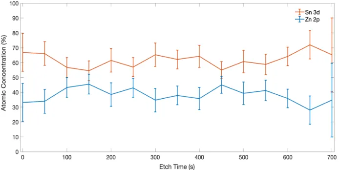
To analyze the constituent layers of the Mo/ZTO/Mo devices, an argon cluster depth profile by X-ray photoelectron spectroscopy (XPS) was used. Throughout the whole ZTO thickness, the Sn/Zn ratio is of 3:2, as can be seen on Figure 4.1, along with the respective error for each etch time. Moreover, it was not possible to observe MoO3 due to the argon beam induced reduction of the material. Therefore in future works, different material analysis tests are needed to evaluate the composition of the interfacial layers.
4.2. Electrical measurements
4.2.1.1. SET and RESET test
After some initial testing, it was found that the VSET polarity is located on the negative side and the VRESET on the positive, however the switching loop of the VRESET seems to happen in an anti-clockwise fashion, which might suggest trapping-like phenomena at the contact interface [38]. This will be explored in detail on the following sub-sections.
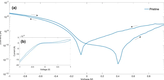
4.2.1.2. Pristine
The pristine curve of a 1x1µm2 device was evaluated by performing a dual voltage sweep of -1V to 1V. On Figure 4.2 the results can be observed for semi-log and linear plots, in which figure (b) shows the rectification characteristics of the Schottky diode.
Figure 4.1 – Atomic concentration (%) of Sn 3d and Zn 2p for different etching times and the associated error.
12
It is important to note that despite the device owning a symmetric structure (two molybdenum contacts and a ZTO layer), the I-V curves are nonlinear. The rectifying characteristic of the device is due to the bottom molybdenum contact that although wasn´t submitted to an oxygen plasma treatment, during the deposition of the ZTO layer on the sputtering chamber, the higher oxygen activity oxidizes the bottom molybdenum contact, forming an interfacial layer of molybdenum ox-ide (MoOx) which due to the high work function creates a Schottky barrier at the vicinity of the MoOx/ZTO layer. Since no oxygen is present during the deposition and etching processes of the top molybdenum contact, these asymmetric conditions result in different barrier properties, there-fore no oxidation occurs on the top contact, providing an Ohmic junction. Hence it can be con-cluded that the sequence of deposition is important, since the different conditions lead to distinc-tive barrier properties at the metal/ZTO as compared to the ZTO/metal interface [12]. The for-mation of an oxide layer depends on the substrate temperature, the type of metal substrate and oxygen activity. However even on inert metals like platinum (Pt) formation of oxides may also occur [12], which indicates that on base metals like molybdenum (Mo), the oxidation of the mate-rial has a higher probability of occurrence upon the production processes.
Analyzing further the pristine, it can be concluded that the device acts in a bipolar fashion and suggests an analog type of switching. Moreover, the hysteresis on figure (b) forms an open loop at 0V, suggesting that the intrinsic parallel capacitance of the device influences the switching behavior [24] [39].
4.2.1.3. Different Voltage Bias Testing
To further evaluate the switching characteristics of the fabricated devices, some tests were per-formed in order to test the limits upon device breakdown. For the VSET, various negative voltage sweeps were performed with crescent values in -1V steps, which can be seen on Annex C. By -5V the device suffers a short circuit and so the maximum voltage was kept at -4V in order to not stress the devices. For the VRESET, the same methodology was used but with 1V steps, seen on Annex D. Again, at 5V the device stops working and thus the following tests were kept at a max-imum voltage of 4V. Since no electroforming step (and therefore no current compliance) was needed in order to reach these results since the device is self-limited, adding to the gradually crescent current states after each application of VSET and VRESET, it is suggested an interfacial type switching as the charge driving mechanism. Besides, with increasing voltages on both VSET Figure 4.2 – (a) Semi Log plot of pristine I-V test for ZTO non passivated for 1x1µm2 device and (b)
Linear plot of same curve. (a)
13
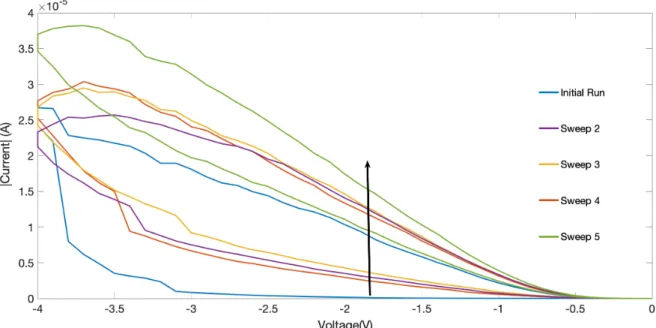
and VRESET, the analog characteristics can be observed and the RESET happens in an anticlock-wise fashion, increasing the current after each sweep behaving like a SET process.4.2.1.4. Multilevel Cell (MLC) Testing
The analog potential of the devices was investigated by performing five consecutive voltage sweeps of -4V for VSET and 4V for VRESET on an 1x1µm2 device. On Figure 4.3 can be observed the VSET process for the consecutive voltage sweeps.
The first application of voltage (initial run) origins a wide value window (initialization), which de-creases after each consecutive sweep. The current after each sweep inde-creases gradually, which suggests a multilevel characteristic, ideal for neuromorphic applications. For the VRESET process, Figure 4.4, the same methodology was applied but with the opposite polarity.
Figure 4.3 - Five consecutive I-V dual voltage sweeps for VSET on a 1x1 µm2 device (clock-wise).
Figure 4.4 - Five consecutive I-V dual voltage sweeps for VRESET on a 1x1µm2 device (anticlock-wise).
14
The current increases after each sweep, therefore no real RESET is detected. Both SET and RESET processes should behave like the converse of one another, like shown on Figure 4.5. But what is observed is that on both polarities a SET process takes place. The timestamp results (current and voltage data vs time) for the sweeps can be accessed on Annex E.
4.2.1.5. The influence of external factors
Since external factors can dictate the performance of the fabricated devices, two tests were per-formed in order to evaluate possible reasons for the anticlockwise RESETswitching: UV influence and vacuum effect.
Vacuum effect
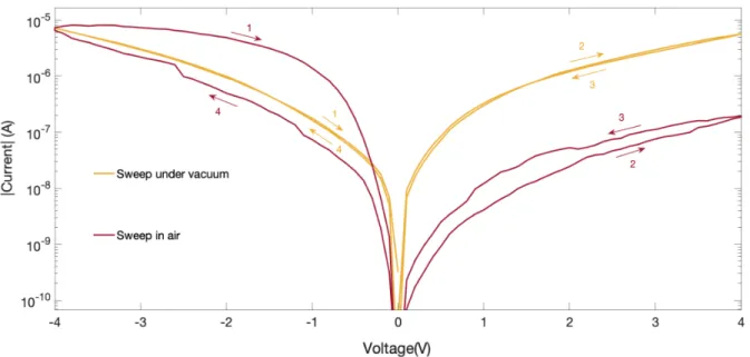
It is well known that amorphous oxide semiconductors (AOS) are highly reactive when in contact with air [41]. To study the influence of this factor, electrical measurements under vacuum condi-tions were carried out and thus the sample was placed under a vacuum level of 10-4 mBar. A device of 10x10µm2 was tested, first performing several VSETs under consequently higher voltages (-1V, -3V, -4V, -5V, -6V) shown in Figure 4.6 and the dual sweep direction checked. The device is more conductive under vacuum and larger voltages can be applied to the device without break-down. The I-V hysteresis is smaller, which when compared to the tests implemented under at-mospheric conditions, suggests that the surrounding ambient conditions influence the resistive switching. Alterations of the resistive switching under different atmospheric conditions are mostly due to the exposed contact’s edges of the samples.
For the VRESET process, a similar procedure was used (1V, 2V, 3V, 4V, 4.5V) and the sweep direction checked as well. The device shows higher current states under vacuum accompanied by a smaller hysteresis, however the sweep direction became clockwise, meaning that the device now shows a correct RESET.
Figure 4.5 – (a) SET and RESET sweeps. Can be noticed the analog increase of conductance during the SET process and decrease during the RESET. (b) Current and voltage data vs time for SET
15
A possible explanation can be found on the levels of moisture present on the device, when being submitted to atmospheric conditions, resulting in corrosion. Like stated by Valov et al. [42], hu-midity despite being present in air and consequently penetrate on the electrode edges, another factor for the incorporation of residual moisture relies on the fabrication processes, some in which use water or other solvents that contain hydrogen species that are therefore assimilated into the ZTO film. It can be speculated that when part of the moisture is removed during vacuum testing, the dominant charge movement mechanism becomes electronic, without excluding possible ion movement.Nonetheless, it has been reported on previous studies [43] that no resistive switching occurs under low moisture levels and dry oxygen conditions, being necessary an extent of humidity to function along with oxygen levels since the mechanism of switching depends on the exchange of oxygen ions with the exterior. The effect of both of these factors can be better observed on Figure 4.7.
Figure 4.6 - VSET (-1V, -3V, -4V, -5V, -6V) and VRESET (1V, 2V, 3V, 4V, 4.5V) I-V under vacuum conditions.
Figure 4.7 – Comparison between a 10x10µm2 device under air and vacuum. The numbers on the arrows represent the sweep direction.
16
The hysteresis strongly depends on the humidity conditions (being much smaller under vacuum than air) and the higher conductivity of the device in vacuum during RESET indicates that a larger quantity of oxygen vacancies (Vo) are present and therefore if ultra-vacuum conditions were to be tested no RESET would occur because the oxygen content in the layer will be insufficientfor the switching to take place [44].
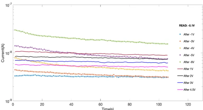
After each VSET and VRESET from Figure 4.6, the retention of the individual states was checked for 100 seconds under a -0.1V read, as can be seen on Figure 4.8, exhibiting the multilevel nature of the device.
Can be also noted that the decay of each SET process follows a close relation to a “stretched-exponential function” (SEF) [33], which mirrors human memory decay. The MLC nature of the device is fundamental for neuromorphic applications, since the gradual update of conductance values (update of synaptic weights) is the core process of synaptic plasticity and thus for learn-ing/forgetting [31]. Moreover the analog update is also important for the matrix-vector multiplica-tion needed for the backpropagamultiplica-tion algorithm used in neural networks, occurring in a massively-parallel fashion [45].
UV influence
The first approach to study the influence of the UV light on the device consisted on the application of dual voltage sweeps from -4V to 4V four times, on a 1x1 µm2 device, while a UV light with a wavelength of 365 nm was used at the contacts’ crossing point (right above the exposed ZTO layer) and the results can be seen on Annex F. Although the RESET direction wasn’t altered, after each sweep for both VSET and VRESET the current level was consequently lower. The same test was carried out without UV and can be noticed on Annex G that without the influence of light, the evolution of the current levels occur conversely to the latter. The current levels lower under UV light, and a possible explanation relies on the generation of a photocurrent due to the release of electrons that have been trapped near the contacts’ interface [46].
17
4.2.1.6. Endurance Testing
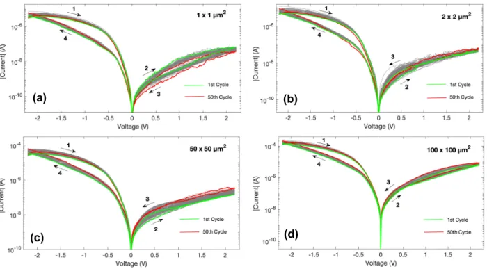
The endurance of the devices was also evaluated, as can be seen on Figure 4.9, by performing 50 cycles from -2V to 2V on four devices with different contact areas: 1x1 µm2; 2x2 µm2; 50x50 µm2; 100x100 µm2.
The cycles were completed successfully without device breakdown, which shows a decent relia-bility. By further analyzing the data on Figure 4.9, it can be noted an unexpected phenomenon: For 1x1 µm2, the RESET behaves properly, being clockwise, unlike what happens on the other device sizes. A possible explanation might be due to alterations caused by the external temper-ature, humidity conditions or the device’s aging, a commonly reported factor among TFTs [47].
However such occurrence wasn’t observed again after additional experiments and the exact causes are open to clarification. It is important to note though, that the as-fabricated devices need some stabilization cycles prior to further testing in order to function more steadily.
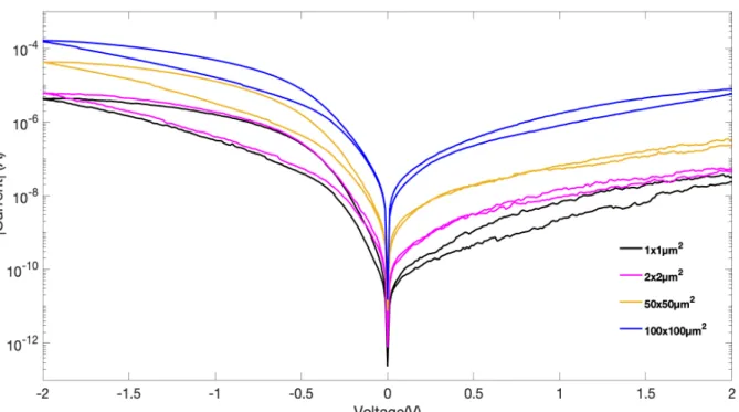
Additionally, it was observed that the current levels differ for different contact areas, which is clearly shown on Figure 4.10 for the 25th cycle. Larger area, larger the current level, which again indicates an interfacial/area dependent type of switching, therefore pointing out to the existence of a Schottky barrier at the interface.
Figure 4.9 – (a) Cycles test for 1x1µm2 device; (b) Cycles test for 2x2µm2 device; (c) Cycles test for 50x50 µm2 device; (d) Cycles test for 100x100µm2 device. Green and red lines show the results for the
first and last cycle respectively.
(a) (b)
18
4.2.1.7. State Retention Testing
To evaluate the retention characteristics of the fabricated devices, ten VSET sweeps were made (-4V) on a 1x1 µm2 device and the final state tested for roughly 12 hours under a VREAD of -0.1V. For VRESET , another 10 sweeps were performed (4V) and the same testing conditions used. The results are depicted on Figure 4.11 in semi-log, where both states differentiate in almost a decade.
Figure 4.11 - State retention test for SET and RESET under a -0.1V VREAD for 12 hours.
Figure 4.10 - I-V comparison for different electrode areas for the 25th cycle. The different current levels suggests the existence of an interface switching mechanism.
19
Again, the SETfollows a stretched-exponential function (SEF) [33] and is more stable than the RESETprocess, the latter showing a noisier subjection to the VREAD process which might be again due to the device’s aging.4.2.1.8. Schottky Junction Properties
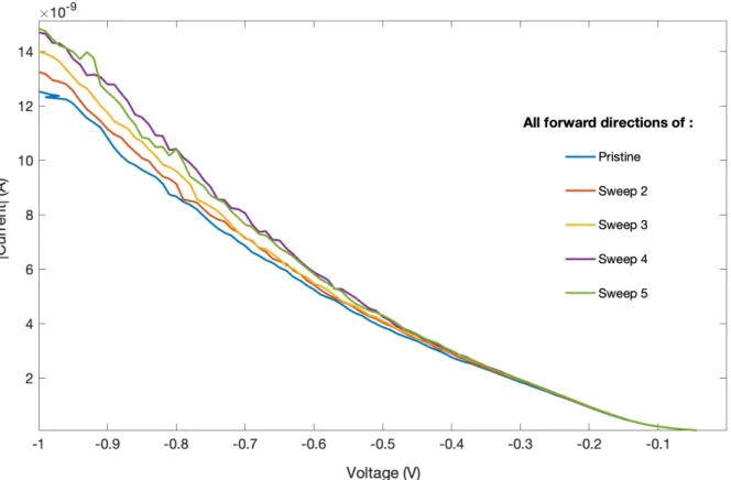
It is relevant to address further the nature of the switching process, by evaluating the Schottky barrier (f), the series resistance (Rs) and the ideality factor (h). For this, five SET dual voltage sweeps were done (-1V) on a 1x1µm2 device and then the linearity of the region was checked. Plot of the LRS of the SET sweeps can be found in Figure 4.12.
It was concluded that is not possible to obtain the parameters based on a semi-logarithmic delin-eation of I/V, since the data is nonlinear. Deviations from “ideal” diodes such as minority carrier injection or recombination within the space charge region among other phenomenon, leads to the masking of the barrier properties of the junction due to the parallel (Rp) and series (Rs) resistance [48]. Therefore the method proposed by Werner [47] was used, in which each parameter was obtained by performing individual fittings using the “LinearModelFit” function from the Mathemat-ica software and the thermionic emission model [49] which accounts for a diode with a series and parallel resistance, given by Equation 3:
1 2345
= A
∗T
8e
f :;∗ <e
=>?∗@A :;h− 1D +
F-GH∗1 2345∗GI(3)
Where h is the ideality factor, T the absolute temperature, A* = 4p e m* KB2 h-3 the effective Richardson constant, K the Boltzmann constant, f the effective barrier height.
Figure 4.12 – The LRS (Low Resistive State) or forward direction of each SET sweep that was used for the fitting.
20
The results are represented on Table 4.1. The parallel resistance was considered infinite for simplification purposes and therefore not calculated.
Table 4.1 - Schottky junction properties for the forward SET sweep.
It is curious to note that the barrier height doesn’t change significantly, demonstrating a random behavior and the high ideality factors for all sweeps show that there are a lot of non-idealities present, such as barrier inhomogeneity due to a non-uniform distribution of the interfacial charges, effects of the series resistance or trap tunneling processes [50] [51].
This underlies other type of conduction mechanism adding to the Schottky barrier tunneling that needs further clarification and the fact that the device is not a simple diode might also contribute to the results observed. Measurements under different temperatures [52] might be a possible future implementation in order to clarify the type of conduction present on the devices.
4.2.2. Zinc Tin Oxide (ZTO) with Molybdenum (Mo) contacts - Passivated
Since ambient moisture affects the devices’ performance, a passivated sample was fabricated on a glass substrate.
4.2.2.1. Pristine Testing
A pristine curve of a 1x1µm2 device is shown on Figure 4.13 in semi log (a) and linear scale (b). The device demonstrates rectification characteristics due to the molybdenum bottom contact, which during production went through an oxygen plasma treatment to create an high function metal electrode (MoOx) to produce a Schottky junction at the interface. The rectification properties of the device were enhanced in comparison with the non-passivated ZTO sample, as seen on Annex H.
This can be due to the passivation process itself or due to the two different techniques used to oxidize the bottom molybdenum contact of the samples (using an oxygen plasma treatment or the higher oxygen activity during the deposition of the ZTO layer). Further investigation is re-quired.
Forward SET Sweep
#Sweep f (eV) h Rs (kW) 1 0,44 17 419 2 0,42 31 291 3 0,42 33 270 4 0,44 28 288 5 0,45 23 357
21
4.2.2.2. Resistive Switching Testing
Following the pristine test, five sweeps for VSET and VRESET were done, for -3V and 3V respectively on the same device, represented on Figure 4.14 and 4.15. The RESET, although still happens in an anticlockwise fashion, seems to show no significant change on the current levels, as seen on Figure 4.15. This might be due to the excellent rectification properties of the device, allowing charges to move during the SETprocess and blocking current flow for the RESET. The current and voltage data vs time results for SET and RESET can be evaluated on Annex I.
Figure 4.14 - Five consecutive dual voltage I-V sweeps for SET on a 1x1µm2 device (clockwise). Figure 4.13 – (a) Semi Log plot of pristine I-V test for ZTO passivated on a 1x1µm2 device and (b)
Linear plot for same curve. (a)
22
4.2.2.3. Endurance Testing
To check the reliability of the new sample, four different devices with different sizes (1x1 µm2; 2x2 µm2; 50x50 µm2; 100x100 µm2) were submitted to 50 endurance cycles (-3V to 3V). The results are represented on Figure 4.16.
Figure 4.15 - Five consecutive dual voltage I-V sweeps for RESET on a 1x1µm2 device (anticlockwise).
Figure 4.16 - (a) Cycles test for 1x1µm2 device; (b) Cycles test for 2x2µm2 device; (c) Cycles test for 50x50 µm2 device; (d) Cycles test for 100x100µm2 device. Green and red lines show the results for
the first and last cycle respectively.
(a) (b)
23
Curiously, for the 1x1µm2 device, the sweep direction for the RESET is correct whilst for the other sizes remains anticlockwise. Nevertheless, such occurrence wasn’t reported on the previous and following tests, which might be due to several factors, as previously mentioned, the temperature and humidity conditions of the laboratory during testing, factors that can disrupt the delicate switching dynamics or even the aging activity of the devices. In addition, considering to implement a process of annealing upon device fabrication might help to stabilize the performance of the samples, a step commonly applied on TFTs for the same purpose, in order to speed up the aging process [53].Furthermore, the passivated devices appear to show more unstable performance than the non-passivated, since the devices with larger sizes suffer from a breakdown before reaching the end of the testing. Such observation indicates that the capacitive property of the devices need to be studied and also confirms that memristors own better performance for smaller sizes [54], which could be the reason why for both passivated and non-passivated devices the VRESET direction is correct for 1x1µm2. Moreover, the devices with larger areas show greater impacts due to the atmospheric parameters, meaning that the passivation layer requires a re-evaluation. Larger sizes also means that the probability of encountering impurities (e.g. dust particles) during pro-duction or testing is higher, causing damage.
4.2.3. Comparison between non-passivated at atmospheric conditions , non-passivated at vacuum conditions and passivated device for RESET
On Figure 4.17, a comparison between a non-passivated device on atmosphere, non-passivated on vacuum and passivated is shown.
Figure 4.17 - Comparison between the RESET process for a ZTO non passivated device under atmospheric conditions (blue); ZTO non passivated device under vacuum (orange); ZTO passivated
device under atmospheric conditions (yellow). The numbers on the arrows represent the sweep direction.
24
The passivated device (1x1µm2) shows the smallest current state (due to a smaller area tested) and noisier RESET. The non-passivated (10x10µm2) device on vacuum shows a higher conduct-ance with a small current window when compared to the non-passivated device tested in air (10x10µm2) and this higher conductance is related to the lower levels of oxygen on the testing chamber. Moreover the device tested on vacuum demonstrates a correct VRESET.
Since passivation wasn’t effective on correcting the RESET issue, the influence of other factors should be investigated, mainly the effect of the passive parallel capacitor, which can strongly influence the dominant model for interface type switching. Being area dependent, this switching can aggravate the effect of the parallel capacitor for larger areas, whilst the smaller ones are governed by the resistive switching model, which adds another possible explanation for the cor-rect switching on the smaller devices from Figure 4.9 (a) and 4.16 (a).
4.2.4. Indium Gallium Zinc Oxide (IGZO) with Molybdenum (Mo) contacts
Due to the impossibility of utilizing the Mo/ZTO/Mo devices derived from the RESET issue, among their erratic behavior upon pulse testing, a new set of devices was fabricated based on IGZO, since this material is reported to own excellent properties for neuromorphic applications [31]. The molybdenum contacts were kept.
4.2.4.1. SET and RESET test
After some initial testing, it was found that the VSET polarity is located on the negative side and the VRESET on the positive, just like on ZTO based devices. The switching loop of the VRESET hap-pens in a clockwise fashion.
4.2.4.2. Pristine Testing
The characteristic pristine state was accessed, by performing a dual voltage sweep (-1V to 1V) on a 1x1µm2 device and the result can be seen on Figure 4.18, for both semi log (a) and linear scale (b). The hysteresis loop, in comparison to the ZTO devices, is much smaller, especially on the SET side, however the RESET shows a correct direction. The rectification property is due to the oxygen plasma treatment of the bottom electrode, however is of worse quality than the pas-sivated ZTO sample. A comparison can be seen on Annex J. Additionally, the static current level is higher on the IGZO device than the ZTO and the current changes sign at +0.8V instead of 0V, suggesting a more significant trapping and detrapping of charges than in the ZTO film [49].
Figure 4.18 – (a) Semi Log plot of a pristine I-V test for IGZO 1x1µm2 and (b) Linear plot of same curve.
(a)
25
4.2.4.3. Multilevel Cell (MLC) testing
A 10x10 µm2 device was submitted to five sweeps for both VSET and VRESET (-3V to 3V) to acknowledge the performance, which are represented on Figure 4.19 and 4.20 respectively. It is clear that the value window for the SET is very small, in comparison with the RESET process, although the initialization step or “first run” demonstrates a wider sweep for both cases. Never-theless, it shows a gradual switching/multilevel, which is needed for neuromorphic computing. The current and voltage data vs time results for SET and RESET can be evaluated on Annex K.
Figure 4.19 - Five consecutive dual voltage sweeps for VSET for 10x10µm2 device (clockwise).
26
4.3. Neuromorphic Applications
Since the IGZO based devices show the best characteristics for neuromorphic applications when compared to the tested ZTO devices, a series of experiments involving pulse testing were carried out. Pulses are used to represent the electrical spikes that occur during message transmission between neurons.
4.3.1. Potentiation and Depression
The connectivity strength between two neurons can decrease or increase over time, depending on the stimulation received and has two values: A positive one (potentiated) and a negative one (depressed). To simulate both situations, 40 pulses for the VSET (-1.5V) and the same number for VRESET (1.5V) were used, representing potentiation and depression respectively, under a -0.1V VREAD, for a 10x10µm2 device. These pulses were fixed at an interval of 10 ms and a width of 100 ms each. The normalized current change is plotted as a function of the number of applied pulses on Figure 4.21, which shows a non-linear asymmetry of the conductance change.
It is reported [55] that an ideal artificial synapse should own a linear and symmetric change of conductance under constant applied pulses, due to the nature of the algorithms used in neural networks (backpropagation algorithm) for maximum accuracy in pattern recognition. However such ideality is not mandatory on a synaptic device: If that characteristic is not met, additional circuits that integrate the read current with multiple pulses can be used with the non-linear device, although the final circuit increases in complexity [56].
4.3.2. Short Term Memory (STM) to Long Term Memory (LTM) transition
It is widely reported on biological systems that upon constant potentiated stimuli, the synaptic weight increases. When such stimuli ceases, the synaptic weight decreases its value. If the final
Figure 4.21 - Potentiated (Blue) and Depressed (Orange) states under a 0.1V VREAD as a function of the number of applied pulses.