A built-in debugger for 1149.4 circuits
Manuel C. Felgueiras1, Gustavo R. Alves1, J. M. Martins Ferreira2
{mcf, gca}@isep.ipp.pt, [email protected]
1
ISEP / LABORIS – Rua Dr. António B. de Almeida – 4200-072 Porto – PORTUGAL
2FEUP / DEEC – Rua Dr. Roberto Frias – 4200-465 Porto – PORTUGAL
Abstract
Debugging mixed-signal circuits is usually seen as a complex task due to the presence of an analog part and the necessary interaction with a digital part. The use of debug and test tools that require physical access suffers from the same restrictions that led to other solutions based on electronic access, especially for digital circuits, due to the increasing operating frequencies and miniaturization scales. This is particularly the case that led to the emergence and wide acceptance of the IEEE1149 family of test infrastructures, which relies on an electronic test access port. While the IEEE1149.4 test infrastructure enables the structural and parametric test of mixed-signal boards, its use is still far from reaching a wide acceptance, namely due to the lack of alternative applications, such as debugging, as it is the case in the 1149.1 domain. This work describes a way to support debug operations in 1149.4 mixed-signal circuits, in particular a built-in condition detection mechanism able to support internal watchpoint/breakpoint operations.
1. Introduction
Mixed-signals (MS) circuits include an analog part and a digital part with an interaction between them. These circuits are rising in importance throughout the last years. Analog circuit design is much more sensitive to implementation details and silicon process variations than its digital counterpart, therefore any critical analog circuitry tends to be a bottleneck in design implementation, verification, and migration to manufacturing of MS circuits [1]. The action of debugging MS circuits intends to detect, locate and diagnose all sorts of errors. Although these operations are very important, especially during the prototype validation phase, circuit miniaturization is constraining the use of debug tools that rely on physical access to implement them. MS circuits have analog and digital inputs/outputs, so electronic access is needed on both domains. This is much less of a problem in the digital domain where several standard infrastructures [2,3] are used directly or exploited as access mechanisms for specific debug circuits [4,5]. In the analog domain, electronic access strategies are still in their infancy. Since the IEEE1149.1 is a well accepted infrastructure to access digital nodes, and considering that 1149.4 [6] extends the former infrastructure for MS circuits, its use for accessing analog nodes in a debug scenario has already been proposed [7,8,9,10]. The present work extends the previous proposals to support watchpoint/breakpoint operations in a debug scenario. In particular, it addresses the implementation and verification of a built-in circuit detection mechanism able to support those operations in both the digital and analog domains. The IEEE1149.4 infrastructure provides the electronic access to this built-in mechanism, namely for selecting the condition to be detected and the node it refers to, thus justifying the title used for this paper, i.e. “A built-in debugger for 1149.4 circuits”. The rest of this paper is organized as follows: section 2 evokes a debug model used for digital circuits and its extension for MS circuits; section 3 describes the condition
detector mechanism in detail; section 4 presents the case study used for verifying (in simulation) the proposed mechanism; section 5 discusses the silicon area penalties; and, finally, section 6 concludes the paper with the final remarks and future directions.
2. Mixed-Signals debug operations
Debugging MS circuits usually requires a collection of tools based on some type of access. Some tools are specific of microprocessor systems, e.g. in-circuit emulators, while others remain generic (logic analyzers, mixed-signal oscilloscopes, multimeters). Each tool can perform a large number of different operations, although all of them belong to a small number of debug operation types. According to a proposed basic debug model [4], any debug operation fits into one of four debug operation types:
- Controllability, Observability, Verification (COV) of the circuit state
- Single Step
- Watchpoins/Breakpoints - Real-time Analysis
The Single Step, the Breakpoint and the Real-time Analysis modes can be used to control/observe/verify the circuit operation in the time domain, while the COV operations can be used to control/observe/verify the circuit state [8]. As an example in the digital domain, e.g. in a microprocessor–based system, suppose we want to verify if a specific data value appears in a certain memory position, when the content of the program counter reaches a certain value. The correspondent debug flow comprises the following steps: (1) clear the defined memory position via a Control operation; (2) place the circuit in normal operation mode and then stop it when the program counter reaches the value specified by a Breakpoint operation; (3) read the specified memory position via an Observation operation; and (4) verify if the observed data matches the expected value via a Verification operation. These very same debug operations can be used in other digital circuit types. For instance, the Breakpoint concept can be applied in a finite state machine-based system, by stopping the clock signal when some condition is validated, forcing the circuit to memorize the actual state, and then using the COV operations to observe and verify the actual values of the circuit state. The Single Step operation can be used in the same circuit to control the clock signal use the COV operations can be used to monitor and verify every single circuit state.
As an example in the MS domain, imagine we want to memorize the circuit state when a specific analog voltage surpasses a predefined limit (i.e. a Breakpoint operation) or that we want to observe in real-time the voltage present at a certain circuit node.Referring to the Breakpoint operation, it involves three distinct phases: (1) the condition specification, (2) the condition detection and, when actually detected, (3) freezing the system. The first sets the equipment to memorize the type of operation and the previously referred limit; the second places the circuit in normal operation until the condition becomes validated; and, three, the circuit must be stopped, forcing it to maintain the actual state, e.g. by stopping
the clock signal in a microprocessor-based circuit. Having in mind that physical access required for several debugging tools is increasingly compromised, a built-in debugger supporting condition detection (i.e. the first two previous mentioned phases) encompasses several advantages to the debug phase. A solution for digital circuits, considering the 1149.1 infrastructure, has already been proposed [4,5]. The present proposal extends its benefits to the MS arena, allowing to relate analog values with digital ones in complex circuits, with a 1149.4 test infrastructure. The generic attributes that we have considered for the condition detector circuit are:
- allow to relate analog with digital values inside the circuit - overcome physical access restrictions
- compatibility with a Std. IEEE1149.4 test infrastructure - minimum overhead, by reusing 1149.4 elements as much
as possible
Figure 1 illustrates one possible situation where the proposed solution helps to debug a MS circuit that includes a microprocessor. An externally clock generator feeds the corresponding clock input pin of a microprocessor, through an AND gate. While the other AND input is logic high the microprocessor will be clocked and execute its normal function. This other AND input is connected to the Valid Condition Output (VCO) pin, which contains the result outputted by the internal MS condition detector circuit. While not in use, the condition detector outputs logic low, and therefore the microprocessor clock is not affected.
Figure 1- Using the mixed-signal condition detector in the breakpoint debug operation.
If a condition is entered and the condition detector detects it, it outputs a logic high at VCO pin, forcing the microprocessor clock to a logic low that will stop its execution.
3. Condition detection for supporting
mixed-signal debug operations through IEEE1149.4
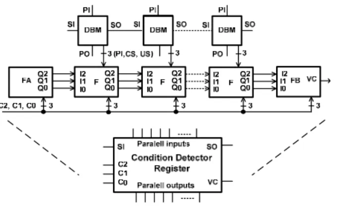
The proposed MS condition detection mechanism reuses the standard IEEE1149.1 boundary scan cell (referred as Digital Boundary Module - DBM - on the IEEE1149.4 Std.) as an elementary one bit comparison block. The DBM illustrated in Figure 2 comprises two memory stages: the Capture/Shift stage (C/S) and the Update stage (U). The first is used to store one limit B/mask bit while the second is used to store one limit A bit. The bit value present at the Parallel Input (PI) will be compared with these limits in the block F. The update stage can be loaded with either a mask or a limit B, depending on the selected condition type. In each block the comparison result is placed on the outputs (Q2,Q1,Q0) and it depends of the:
Figure 2-The DBM and the associated block F. - actual bit to be compared (PI)
- specific A/B bit limits stored on the cell (C/S,U) - previous block F comparison result (I2,I1,I0) - selected comparison operation (C2,C1,C0)
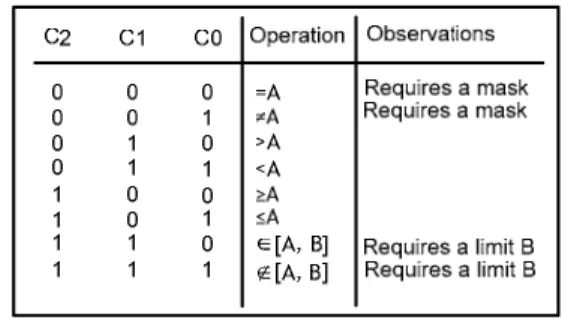
The result present at (Q2,Q1,Q0) corresponds to one of five possibilities: False, True, Equal to A, Great than A, or Less than B; so that three lines (23) are needed to codify all these
possibilities. The total number of possible comparison operations performed by block F is eight, as listed in Table 1.
Table 1- List of all operations performed by block F.
For each operation there is a unique truth table, the corresponding function being implemented by the block F, that considers inputs (C2,C1,C0), (I2,I1,I0), and the C/S, U and PI values to calculate the values outputted at (Q2,Q1,Q0). As an example, Table 2 presents the truth table for the “=A” operation, which is selected when (C2,C1,C0) = (0,0,0).
Table 2- Truth table of the block F for the “=A” operation.
The remaining seven truth tables are selected according to the contents of (C2,C1,C0), as shown in the Table 1, and are not represented here for space reasons. The several blocks F are cascaded, in a similar way to the correspondent DBMs, and all together form the Condition Detector Register, as illustrated in Figure 3. This register works as a digital word comparator where the final result is placed at the Valid Condition (VC) output.
Figure 3- The Condition Detector Register and it simplified representation.
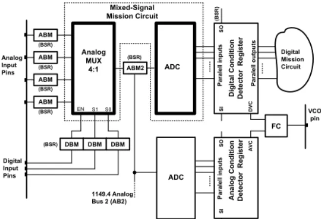
As MS circuits have analog and digital input/output nodes, we use two of these registers (i.e. an Analog Condition Detector Register and a Digital Condition Detector Register) to detect conditions in both domains, as shown in Figure 4. The standard IEEE1149.4 infrastructure is used to select the analog node (pin, or internal node as proposed in [8]) under analysis and its value is converted into a digital word by an additional Analog to Digital Converter (ADC) that is part of the present proposal. The ADC digital outputs are compared against the limits previously stored in the Analog Condition Detector. Notice in Figure 4 that the Analog Condition Detector Register has no parallels outputs, so DBMs without the 2nd MUX can be
used to build it Register, to support the watchpoint/breakpoint operation in the analog domain.
Analog Condition Detector Register Paralell inputs SI SO AVC C2A C1A C0A 1149.4 Analog Bus 2 (AB2) ADC (TDI) (TDO) From the Detection Configuration Register From the Detection Configuration Register FC VCO pin VS1 VS0 From the Detection Configuration Register Digital Condition Detector Register Paralell inputs Paralell outputs SI SO DVC C2D C1D C0D (TDI) (TDO)
Figure 4- The Analog and Digital Condition Detectors arrangement for MS circuits.
The Digital Condition Detector Register is used directly in the digital input/output pins or internal nodes located in the analog/digital mission circuit interface and is formed by the already existing DBMs. Notice that for the digital condition detection, it is possible to reuse the capture/shift and the update stages of the DBMs to store the limits B and A since they are not in operation when the circuit is working in normal mode (except for the sample functionality provided by the
SAMPLE/PRELOAD instruction). For an Analog Boundary
Module (ABM) the scenario is different because its switch infrastructure state depends on every instant from the associated control register information, so it cannot be reused to store the analog detection limits. The block FC presented in Figure 4 (right side) is responsible for selecting the signal that feeds the VCO pin, according to the conditions presented in Table 3.
Table 3- Truth table for the VCO pin value.
In short, it allows selecting either the result of the analog or digital condition detection or a logic combination (AND, OR) of both signals. The COMP2 signal listed in Table 3 is logic high when the Instruction Register (IR) is loaded with either instructions EXTEST2, PROBE2, or INTEST2 (described later in this paper), while RTI corresponds to a signal that is logic high when the TAP controller is in the Run-Test/Idle state. These two signals (CMP2, RTI) guarantee that the condition detector only works when one of the comparison instructions referred above is loaded in the Instruction Register (IR) and the TAP Controller is in the Run-Test/Idle state. The AND/OR possibility for the Analog and Digital Valid Condition signals - AVC/DVC - (two last rows in Table 3) is selected by the VS0 and VS1 bits of the Detection Configuration Register and corresponds to additional trigger functionalities present in some mixed-signal oscilloscopes. The operation performed by the blocks F present inside the Analog/Digital Condition Detector Registers is selected by the (C2,C1,C0) bits, independently for the analog and digital types, as illustrated by Figure 5. The separate selection options require six bits, i.e. three bits for the digital condition type (C2D,C1D,C0D) and three bits for the analog condition type (C2A,C1A,C0A).
Figure 5- The Detection Configuration Register bits assignment.
Summing up the proposed registers, Figure 6 presents the new register structure for an IEEE1149.4-compatible component supporting the functionality proposed in this work. The main differences are: an optional register named Detection Configuration Register, and the Analog Condition Detector Register that contains the condition values for the analog part. The Digital Condition Detector Register is based on the DBMs already present in the circuit test infrastructure, which together with the TBIC and the ABMs control registers form the Boundary Scan Register (BSR), illustrated in Figure 6.
Figure 6- IEEE 1149.4 register structure resulting from the present proposal.
The BSR is selected by the mandatory and optional 1149.4 instructions EXTEST, SAMPLE/PRELOAD, PROBE, and
instructions that selects the BSR and the Analog Condition Detector Register (data mux input 2): EXTEST2,
SAMPLE/PRELOAD2, PROBE2, and INTEST2. The SAMPLE/PRELOAD2 instruction is used to load the Limit A
value into the update stage of the Analog/Digital Condition Register, so apart from the previous referred difference it works exactly as the mandatory SAMPLE/PREOLAD instruction. The EXTEST2, PROBE2, and INTEST2 instructions have similar functionality to the instructions defined in the standard with the difference that, when active, they cause the UpdateDR signal feeding the update stage to be disabled, in the Analog/Digital Condition Detector Registers. This allows the mask or limit B to be stored in the capture/shift stage, while not overwriting the information previously stored in the update stage (limit A) when the TAP controller moves through the Update-DR state. Finally, the additional SELCON instruction places the Detection Configuration Register in the TDI-TDO path, allowing the user to specify, via the Test Access Port, the analog and digital condition types and function present at VCO.
4. Verifying the detection mechanism: a case
study
The built-in condition detector has been simulated in the ORCAD environment. As illustrated in Figure 7, the target MS mission circuit consists of an analog multiplexer 4:1 and an ADC converter, depicted in bold. The complete MS circuit therefore includes: the target MS mission circuit; the IEEE1149.4 infrastructure and its extension mechanisms to access internal analog nodes, as described in [8]; and the additional debug circuitry presented in this paper. The circuit exhibits the following characteristics: the analog input pins have standard ABMs; the digital input pins have DBMs; in the middle node situated between the analog multiplexer output and the ADC input there is an ABM2 compatible with the modules proposed in [8], which allows fully observability and controllability through the AB1/AB2 lines; in the interface between the analog/digital mission circuit nodes the IEEE1149.4 recommends the use of DBMs (mandatory if the device supports the INTEST instruction), so we have used them to build the Digital Condition Detector Register (if the detection feature is not used, these DBMs will play their regular role within the BSR circuit); the Analog Condition Detector Circuit and the associated ADC is part of the internal test infrastructure and is used to detect analog conditions.
(BSR) ABM2 (BSR) ADC Analog MUX 4:1 Mixed-Signal Mission Circuit ABM (BSR) ABM (BSR) ABM (BSR) ABM (BSR) EN S1 S0 Analog Input Pins ADC Digita l Condition De te ct or Re gi s te r Par alel l input s Par al ell out put s SI SO DVC (B S R ) Digital Input Pins Digital Mission Circuit 1149.4 Analog Bus 2 (AB2) DBM DBM DBM FC VCO pin Ana log Condition De te ct o r R e g ist er Pa ra le ll inpu ts SI SO AVC
Figure 7- MS circuit used for verification purposes.
In order to illustrate the condition detector operation, we present the case where “ [A,B]” is used as the analog detect condition in the analog node associated to ABM2. In this case, VCO goes high when the voltage present at the analog node under analysis is within the -1 V and +5 V limits, and low if else (i.e. if the ABM2 node voltage is below -1 V or if it is above +5 V, VCO will remain at logic low). To select this operation, we first characterize the content of the Detection Configuration Register, i.e. the (C2A,C1A,C0A), (C2D,C1D,C0D) and (VS1, VS0) values. For the first two sets we refer Table 1 and for the third Table 3. In the proposed example we use “ [A,B]” as the analog detection operation, so the first set should be (C2A,C1A,C0A) = (1,1,0), and no digital detection operation, so the second set should be (C2D,C1D,C0D) = (X,X,X). The third set should be (VS1,VS0) = (0,1), which corresponds to the VCO being dependent, only, the analog detection result, as expressed in the previous sentence. Notice that the content of the second set (C2D,C1D,C0D) is irrelevant since DVC is not considered in the final detection result present at the VCO pin. The defined vector content (C2D,C1D,C0D,C2A,C1A,C0A,VS1,VS0) = (XXX11001) is shifted to the Detection Configuration Register using the new SELCON instruction. Next, we have to convert limits A and B, indicated as analog values, into the corresponding digital words and shift them into the Analog Condition Detector Register. Limit A will be shifted in first place using the new SAMPLE/PRELOAD2 instruction. Limit B is shifted afterwards using the new PROBE2 instruction. While this instruction is active the detection process starts the moment the TAP controller enters the Run-Test/Idle state. The following paragraph illustrates, in pseudo-code, the steps required for configuring the 1149.4 test infrastructure with the described parameters.
Instruction Register SELCON;
%Select position 0 in the Data MUX (see Figure 6);
Detection Configuration Register (C2D,C1D,C0D,C2A,C1A,C0A,VS1,VS0) (XXX 110 01);
%Shift the vector that selects the analog condition type % and the analog detection to be outputted in the VCO pin; Instruction Register SAMPLE/PRELOAD2;
%Select position 2 in the Data MUX;
BSR + Analog Condition Detector Register (XXX...analog_limitA); %Shift the vector that selects the analog node under %analysis and the limit A for the Analog Condition %Detector Register. The digital value that corresponds to %-1V is shifted into the Analog Part.
Instruction Register PROBE2;
%Select position 2 in the Data MUX;
BSR + Analog Condition Detector Register (XXX...Analog_limitB); %Shift the vector that selects the analog node under %analysis and the limit B for the Analog Condition Detector Register. The digital value that corresponds to +5V is shifted into the Analog Part.
TAP controller Run/Test Idle;
To run this simulation in the ORCAD environment in a smooth way, we developed in-house a specific application, named BSOrcad, which automatically generates the TCK, TMS, and TDI signals. This application accepts as input a test program written in a high level language, similar to SVF. The test sequences are converted into digital levels for each of the TAP input signals, in the time domain (used in simulation). The application produces, as an output, a stimulus file <name>.stl accepted by the ORCAD. The simulation results for the previous requirements are shown in Figure 8, where the following signals are displayed:
TCK TAP controller coded state TMS Instruction Register content
TDO VCO output pin Analog signal at AB2 (IEEE1149.4)
As expected, the VCO pin is logic high when the cumulative requirements are satisfied: the analog voltage values in the selected analog node belong to the pre-defined interval [-1V, +5V]; instruction PROBE2 (07h) is active; and the TAP
controller is in Run/Test-Idle. From Figure 8 it is possible to observe that the TAP controller changes to the Run/Test-Idle, a state coded as Ch, at 3,5 ms.
Figure 8- The VCO pin response for a sine wave present at AB2 and a [-1V;+5V] selected condition. This example is presented to illustrate the detector condition
function. Other configurations can be implemented to support breakpoint operations. Notice that the VCO remains at logic low until the detector condition circuit changes it, which happens when a valid condition is met. To use the VCO pin as a breakpoint control signal, as earlier suggested in Figure 1, the condition to be met should correspond to the intended breakpoint condition.
5. Area penalties
The area overhead is generally presented as a percentage of silicon expended for some extra-circuit. For the IEEE1149.4 infrastructure this overhead depends on two factors: a fixed one that includes the TAP controller, the IR, the Instruction Decoder, the TBIC switching and control structures, among other fixed blocks; and a variable one that depends on the number of total nodes with ABMs or DBMs. In this section, we consider the overhead introduced by the condition detection circuit in relation to the mandatory 1149.4 test infrastructure. In the simulated circuit we have used some of the ABMs proposed in a previous work [8], and therefore we decided to consider it as part of the “mandatory” 1149.4 test infrastructure for the sake of the overhead calculations presented in the following paragraphs. In the present calculus we assumed the following:
- all digitals circuits are decomposed into elementary gates with two inputs (G2)
- all elementary gates with two inputs (G2) have similar complexity
(this is not the case with XOR or X-NOR gates, but very often the number of these gates - if used - is only a small percentage of the total number of equivalent gates present in the circuit). In this way, the complexity of some test infrastructure blocks is:
TAP controller N(G2) = 159 1 bit IR N(G2) = 37 8 bit IR N(G2) = 296 Bypass register N(G2) = 17 Instruction Decoder N(G2) = 62 DBM N(G2) = 41
ABM (digital part) N(G2) = 165
where N(G2) represents the number of G2 gates necessary to
build each considered block. An 1149.1 test infrastructure has therefore a complexity of:
N(G2) = 556+41NDBM
expressed in G2 gates, where NDBM represents the total
Example 1: for an Integrated Circuit (IC) equipped with an IEEE1149.1 test infrastructure, with 100 DBMs, the equivalent complexity is equal to N(G2) = 4656. That means
this IC test infrastructure can be built using 4656 two-input gates. An 1149.4 test infrastructure comprehends a digital part, which can be expressed in a number of G2 gates, and a certain number of switches and comparators. Depending on the used technology, each of these elements (G2 gates, analog switches and comparators) has an associated silicon area. In this paper the circuit complexity is presented in simple terms of these elements, i.e. G2 gates, analog switches and comparators. An 1149.4 test infrastructure has therefore a complexity of:
N(G2, SWITCHES,COMPARATORS) =
(746+165 NABM+41 NDBM , 10+6NABM , 2+NABM )
where NABM represents the number of ABMs. The former
values include the TBIC switching and control structures, which are fixed blocs, i.e. they are independent of the number of pins in the target-IC.
Example 2: for an IC equipped with an IEEE1149.4 test infrastructure, with 100 DBMs and 5 ABMs, the equivalent complexity is equal N(G2, SWITCHES,COMPARATORS) =
(5671,40,7). An 1149.4 test infrastructure supporting the proposed MS condition detector circuit has therefore a complexity of:
N(G2, SWITCHES,COMPARATORS) =
(1091+165NABM+41NDBM+119NDREG+115NAREG ,
10+6NABM , 2+NABM ]
where NDREG and NAREG represents the number of bits in the
Digital Condition Detector Register and Analog Condition Detector Register, respectively. Further, an ADC whit NAREG
bits is added to the infrastructure.
Example 3: Consider an IC equipped with an IEEE1149.4 test infrastructure supporting the proposed MS condition detection circuit with NABM=5, NDBM=92, NDREG =8, NAREG
=8 (these figures have been chosen to permit the comparison with the results provided in example 2; we assume that the Digital Condition Detector Register has been built reusing the 8 existent DBMs). The equivalent complexity of this infrastructure is now equal N(G2, SWITCHES,COMPARATORS) =
(7560,40,7). These examples permit to conclude that for the ICs considered in examples 2 and 3, the condition detector circuit introduces a digital overhead of 33% in the 1149.4 infrastructure. Notice that the number of switches and comparators remains the same. The main difference corresponds to the introduction of the 8 bit-ADC, which was not considered in our overhead calculus, as it may be implemented in different ways. The ADC complexity may in fact correspond to an unacceptable overhead. However, this should always be compared in addition to the overhead already calculated and presented in this paper, to the benefits encompassed by the proposed debug capability. The cost of an increased area overhead may actually be overcome by the benefits associated with a reduced debug cycle, which will obviously reduce the time-to-market.
6. Conclusions
The work described in this paper addresses the problem of detecting mixed-signal conditions to support debug operations. Many MS debug tools rely on physical access and this is more and more compromised with the recent advances on miniaturization scales and operating frequencies. The proposed built-in condition detection circuit reuses the IEEE1149.4 test infrastructure for storing the limit values for the condition detector circuit, selecting the analog node under analysis, and configuring the detection circuit. As a response, the detector circuit outputs at the VCO pin a signal that can be used to implement watchpoint/breakpoint operations. The ORCAD simulation environment has been used to validate the proposed MS condition detector. The built-in test circuit includes a target MS circuit, the IEEE1149.4 test infrastructure and the MS condition detector. The main limitation of the proposed MS condition detector is the overhead introduced in relation to the standard IEEE1149.4 infrastructure. The overhead introduced has been measured in terms of two-input equivalent gates (G2), in relation to the digital part, as the analog is measured in terms of switches and comparators, remains the same. For an IC with an 1149.4 test infrastructure with 100 DBMs, 5 ABMs, 8 bits for Digital Condition Detector, 8 bits for the Analog Condition Detector, the penalties consist of 34%, in terms of digital complexity, plus an 8 bit ADC. Future work includes the performance characterization of the proposed detection circuit, alternatives applications for field maintenance, and new 1149.4-compliant built-in circuits to support other MS debug operations.
7. References
[1] “The Rise of Digital/Mixed-Signal Semiconductors and Systems-on-a-Chip”, Cadence White Paper, 2002.
[2] IEEE Standard Test Access Port and Boundary-Scan Architecture, October 1993, IEEE Std. 1149.1, ISBN 1-55937-350-4.
[3] NEXUS-ISTO 5001, Industry Standards and Technology Organization, 2003
[4] G. Alves, J. M. M. Ferreira “From for-Test to Design-for-debug-and-Test: Analysis of Requirements and Limitations for 1149.1”, Proceedings of the 17th IEEE VLSI Test
Symposium, 25-29 April 1999, pp. 473-480.
[5] G. Alves, J. M. M. Ferreira “Using the BS register for capturing and storing n-bit sequences in real-time”, Proceedings of the European Test Workshop, 25-28 May 1999, pp. 130-135. [6] IEEE Standard for a Mixed-Signal Test Bus, March 2000, IEEE
Std. 1149.4, ISBN 0-7381-1755-2.
[7] M. Felgueiras, G. Alves, J. M. M. Ferreira “A Built-in Mixed-signal Block Observer (BIMBO)”, Proceedings of the 9th IEEE
European Test Symposium, 23-26 May 2004, pp 105-106. [8] M. Felgueiras, G. Alves, J. M. M. Ferreira “Debugging
mixed-signals circuits via the IEEE1149.4-analysis of limitations and requirements” Proceedings of the International Mixed-Signals Testing Workshop, 21-23 Jun 2006, pp 2-7.
[9] U. Kac, F. Novak, F. Azais, P. Nouet, M. Renovell “Extending IEEE1149.4 Analog Boundary Modules to Enhance Mixed-Signal Test”, IEEE Design & Test of Computers March-April 2003, pp 32-39.
[10] U. Kac, F. Novak, S. Macek, M.S. Zarik, “Alternative Test Methods Using 1149.4” Proceedings of the Design, Automation and Test in Europe, 27-30 March 2000, pp 463-467.
![Figure 8- The VCO pin response for a sine wave present at AB2 and a [-1V;+5V] selected condition](https://thumb-eu.123doks.com/thumbv2/123dok_br/18199186.875952/6.892.131.798.220.667/figure-vco-response-sine-wave-present-selected-condition.webp)