UNIVERSIDADE DO ALGARVE
Electrical characterization of metal-oxide-polymer
devices for non-volatile memory applications
Paulo Roberto Ferreira da Rocha
PhD thesis in Electronics and Telecommunications
Scientific area: Electronics and Optoelectronics
Work done under the supervision of:
Prof. Dr. Henrique Leonel Gomes
iii
Statement of Originality
Statement of authorship: The work presented in this thesis is to the best of my
knowledge and belief, original, except as acknowledge in the text. The material has
not been submitted, either in whole or in part, for a degree at this or any other
university.
Candidate:
__________________________________________________
(Paulo Roberto Ferreira da Rocha)
Copyright ©Paulo Roberto Ferrreira da Rocha. The Universidade do Algarve has
the perpetual right, without geographical limits, of archiving and publicizing this
thesis in all forms, printed or in paper, digital or any other known or hereafter
developed form. This transfer includes the right to provide the thesis through
scientific repositories and the right to admit its copy and distribution with
v This work was financially supported by the Dutch Polymer Institute (DPI), Project
No. 704, BISTABLE (resistive switching and OLED reliability) and by Fundação
vii
Acknowledgments
Great things in life come with great effort and a bit of luck. Personally, I have been extremely lucky to have so many important people to guide my effort. My supervisor has undoubtedly been my mentor. Our fruitful discussions motivated me to understand and further my work. Professionally and personally, Prof. Henrique always showed dedication, respect and willingness to help. I also had the great privilege to discuss scientific results (among many other topics) with excellent worldwide researchers such as Dago de Leeuw, Stefan Meskers, John Vaan Haare, Frank Verbakel, and Lode Vandamme. I owe them my gratitude. Furthermore, I am extremely grateful to José Giacometti for the precious help and amazing guidance. I would also like to give special thanks to Prof. Carmo Medeiros. I am forever thankful for her willingness to train me and her belief in me.
I would like to thank my colleagues and friends that directly or indirectly helped me to cross some motivational barriers. I speak of Ricardo Avó, José Coimbra, Mark Guerreiro, Alvaro Barradas, Pedro Inácio, Ana Mestre, Joana Canudo, Qian Chen, Benjamin Bory and Aldric Negrier. Special thanks to my acting group which has been a great support during these last few years. Thank you so much Emilio and Felicidade Croa for teaching me to perform on the stage of life and for your ever present care and affection. And of course, thank you my very dear and precious friend, José Cabecinha.
Without love, life would be shallow, empty, and void of happiness and adventure. I am blessed to have found someone to be my life companion, Ida Gaspar. Through her understanding, motivation and presence, barriers became easier to cross. My parents, João and Neyde Rocha, are undoubtedly the best parents I could have. They never stopped believing and supporting my decisions. Thank you so much to my dear sister Raquel. During my PhD, you sailed to another place. I am sure you will be smiling from up above regarding my life accomplishments. Foste e serás eternamente um motivo de orgulho e uma lição de vida para todos os que se cruzaram contigo. Obrigado pelo teu apoio. I am also thankful for the support, motivation and love of my sister, Solange, and brother, João. Furthermore, thank you Fernando, Jessica, Pedro, Delfina, Samuel, Cláudia, Manuel and Olinda for your understanding and special care during these last few years. I am blessed to have you all in my life.
ix
Abstract
The objective of this thesis is to study the properties of resistive switching effect based on bistable resistive memory which is fabricated in the form of Al2O3/polymer diodes and to contribute to the elucidation of resistive switching mechanisms.
Resistive memories were characterized using a variety of electrical techniques, including current-voltage measurements, small-signal impedance, and electrical noise based techniques. All the measurements were carried out over a large temperature range. Fast voltage ramps were used to elucidate the dynamic response of the memory to rapid varying electric fields. The temperature dependence of the current provided insight into the role of trapped charges in resistive switching. The analysis of fast current fluctuations using electric noise techniques contributed to the elucidation of the kinetics involved in filament formation/rupture, the filament size and correspondent current capabilities.
The results reported in this thesis provide insight into a number of issues namely: (i) The fundamental limitations on the speed of operation of a bi-layer resistive
memory are the time and voltage dependences of the switch-on mechanism. (ii) The results explain the wide spread in switching times reported in the
literature and the apparently anomalous behaviour of the high conductance state namely the disappearance of the negative differential resistance region at high voltage scan rates which is commonly attributed to a “dead time” phenomenon which had remained elusive since it was first reported in the ‘60s.
(iii) Assuming that the current is filamentary, Comsol simulations were performed and used to explain the observed dynamic properties of the current-voltage characteristics. Furthermore, the simulations suggest that filaments can interact with each other.
(iv) The current-voltage characteristics have been studied as a function of temperature. The findings indicate that creation and annihilation of filaments is controlled by filling and neutralizing traps localized at the oxide/polymer interface.
(v) Resistive switching was also studied in small-molecule OLEDs. It was shown that the degradation that leads to a loss of light output during
x
operation is caused by the presence of a resistive switching layer. A diagnostic tool that predicts premature failure of OLEDs was devised and proposed.
Resistive switching is a property of oxides. These layers can grow in a number of devices including, organic light emitting diodes (OLEDs), spin-valve transistors and photovoltaic devices fabricated in different types of material. Under strong electric fields the oxides can undergo dielectric breakdown and become resistive switching layers. Resistive switching strongly modifies the charge injection causing a number of deleterious effects and eventually device failure. In this respect the findings in this thesis are relevant to understand reliability issues in devices across a very broad field.
Keywords: Memristor, Negative Differential Resistance (NDR), Resistive Switching,
Noise measurements, Electrical characterization, Resistive random Access Memories
xi
Resumo extenso
As memórias resistivas baseiam-se na alteração da resistência elétrica de um material ou componente quando submetido a uma tensão elétrica. Este fenómeno deu origem a um novo elemento eletrónico que se passou a designar por “memristor” por sugestão de Leon Chua em 1971. [1] O “memristor” juntou-se assim aos componentes elétricos mais conhecidos, o condensador, a bobine e a resistência.
Desde os anos 60 que a comutação resistiva tem sido observada numa variedade de materiais. No contexto desta tese os mais interessantes são por exemplo o SiOx, Al2O3, Ta2O5, ZrO2 e TiO2, onde a comutação resistiva é um processo eletrónico e não envolve uma mudança de fase do material.
Os processos físicos envolvidos na comutação de resistência tem permanecido pouco claros. Os vários mecanismos propostos não tem merecido o consenso da comunidade científica. A ausência de um modelo físico tem impedido o desenvolvimento tecnológico destas memórias que têm assim progredido de forma empírica.
Apesar da falta de conhecimento sobre os mecanismos físicos, as memórias resistivas oferecem um conjunto de vantagens sobre as tecnologias atuais. Isto despoletou uma intensa atividade de pesquisa quer no meio académico quer pela industria para comercializar este tipo de componente. As memórias resistivas combinam num só componente as vantagens de diversas tecnologias atuais. Podem ter a velocidade de acesso das memórias aleatórias de acesso dinâmico (DRAMs) com um custo muito inferior, com menor consumo de energia e sem necessidade de periodicamente fazer o restauro ou “refeshing”. Oferecem as características não-voláteis de uma memória do tipo “flash”, mas mais robustas, permitindo assim mais ciclos de leitura e escrita. Possibilitam uma elevada densidade e não sofrem dos problemas mecânicos dos discos duros associados com as cabeças de leitura.
A comercialização deste tipo de memórias irá revolucionar as tecnologias de informação ao disponibilizar uma elevada capacidade de memória a baixo custo, em dimensões reduzidas e com muito baixo consumo de energia. As memórias resistivas também não precisam de alguma da eletrónica que acompanha os sistemas atuais, nomeadamente os sistemas de “cache”, reduzindo substancialmente os custos e a complexidade dos circuitos.
xii
O trabalho desenvolvido nesta tese foi focado nas propriedades elétricas das memórias resistivas com o objetivo de aumentar o nosso conhecimento sobre os mecanismos físicos e elétricos que controlam a comutação resistiva e a velocidade de acesso.
As memórias estudadas nesta tese são estruturas do tipo metal-isolador-semicondutor (MIS). Foi usado óxido de alumínio e um polímero conjugado para a camada isolante e semicondutora respetivamente. Estas memórias comutam entre dois estados resistivos diferentes quando submetidas a voltagens definidas durante um certo período de tempo. Paralelamente, foi identificado que o processo físico que conduz a bi-estabilidade elétrica do óxido de alumínio é também responsável pela falha prematura de díodos emissores de luz orgânicos (OLEDs). A presença de óxido de alumínio nativo nos eletrodos dos OLEDs pode dar origem a transições resistivas que alteram o equilíbrio da injeção de portadores de carga e leva a degradação da eletroluminescência. Quer as memórias quer os díodos emissores de luz foram caraterizados usando técnicas elétricas e óticas. Medidas da resposta da corrente a degraus e/ou rampas de tensão permitiram avaliar a velocidade de comutação resistiva. Medidas da impedância no domínio da frequência foram usadas para estudar variações de carga nas interfaces da memória, e por último medidas do ruído elétrico complementadas com medidas óticas permitiram estudar flutuações na corrente causadas pela criação e aniquilação de pequenos caminhos condutores ou filamentos. Todas as medidas foram feitas num grande intervalo de temperatura e frequência.
Esta tese contribui para o esclarecimento dos mecanismos físicos que originam comutações entre estados resistivos não-voláteis. As constantes de tempo que controlam o tempo de acesso à memória, isto é, o tempo para ler, escrever ou apagar foram também estudadas. Os resultados obtidos contribuíram para elucidar o mecanismo físico que determina o tempo de acesso. Estratégias para otimizar a rapidez deste tipo de memoria foram propostas. Foi identificado que a condução elétrica é não-homogénea. A corrente é transportada por filamentos. Foi possível quantificar as dimensões físicas e a densidade de corrente transportada por filamentos individuais. O estudo da dinâmica destes filamentos usando técnicas de análise de ruído elétrico permitiu concluir que os filamentos não são criados nem destruídos, mas sim ligados e desligados como interruptores. O mecanismo que liga os filamentos são buracos armadilhados na camada
xiii
de óxido de alumínio. Quando os buracos são neutralizados por eletrões o filamento é desligado. Este resultado foi um dos contributos mais importantes para a área científica. A condução filamentar dá origem a um conjunto de observações não intuitivas. Concretamente, dá origem a uma dependência anómala da corrente elétrica com a temperatura. A corrente aumenta de forma discreta à medida que a temperatura diminui, isto porque o armazenamento de cargas em armadilhas a baixas temperaturas liga mais filamentos. Adicionalmente, a existência de condução filamentar dá origem a que a corrente elétrica diminua, quando as rampas de tensão rápidas são aplicadas sucessivamente. Os resultados desta tese também sugerem que filamentos de corrente vizinhos podem interatuar e dar origem a fenómenos correlacionados, quer durante o ligar, quer durante o desligar de filamentos. O campo elétrico associado a dois filamentos vizinhos induz um campo elétrico adicional na região intermédia que pode ligar um terceiro filamento. Se um filamento for desligado os filamentos na vizinhança terão mais probabilidade de ser desligados. Simulações usando o “COMSOL Multiphysics” parecem suportar a correlação destes fenómenos.
A comutação resistiva é uma propriedade de óxidos binários. Este fenómeno pode ocorrer de forma não intencional, nomeadamente em díodos emissores de luz, células solares, válvulas de spin, transístores de efeito de campo e de uma forma geral, todos os componentes que usam elétrodos que oxidam. O conhecimento adquirido nesta tese é assim relevante para detetar e prevenir problemas de confiabilidade num conjunto vasto de componentes eletrónicos.
xv
Contents
Statement of Originality ... iii
Acknowledgments ... vii
Abstract ... ix
Resumo extenso ... xi
1. Introduction ... 2
1.1. Memory devices ... 2
1.1.1. State of the art ... 2
1.1.2. Flash memories ... 4
1.2. Resistive switching ... 6
1.2.1. Resistive switching ... 6
1.2.2. Categories of resistive switching ... 7
1.2.3. Materials for RRAMs ... 9
1.3. Resistive switching models ... 9
1.4. Aim of the thesis ... 12
2. An equivalent circuit model for a metal-oxide polymer diode ... 16
2.1. Introduction ... 16
2.2. Device physical structure and equivalent circuit model ... 16
2.2.1. Limits for the RRAM in LRS and HRS ... 19
2.2.2. The time constants ... 20
2.2.3. The frequency dependence admittance of the diode ... 21
2.3. Conclusion ... 22
3. The role of internal structure in the anomalous switching dynamics of metal-oxide polymer resistive RAMs ... 24
xvi
3.2. Experimental ... 25
3.3. Results and Discussion ... 26
3.3.1. Transient response of the HRS ... 26
3.3.2. Transient response in the LRS ... 28
3.3.3. Hot-spots and the NDR ... 34
3.3.4. Scan-rate dependence of the NDR region ... 35
3.3.5. Implication for device design ... 37
3.4. Conclusion ... 38
4. Anomalous temperature dependence of the current in metal-oxide polymer resistive RAM ... 40
4.1. Introduction ... 40
4.2. Experimental ... 40
4.3. Results and discussion ... 41
4.3.1. IV characteristics of the RRAM ... 41
4.3.2. Thermal behaviour in the HRS ... 41
4.3.3. Thermal behaviour in the LRS ... 42
4.3.4. Small-signal impedance measurements ... 44
4.4. Conclusions ... 47
5. Low-Frequency diffusion noise in Resistive-Switching Memories Based on Metal-Oxide Polymer Structure ... 50
5.1. Introduction ... 50
5.2. Experimental ... 51
5.3. Results and Discussion ... 51
5.3.1. IV characteristics of the RRAM ... 51
5.3.2. Definition of charge injection regimes ... 52
5.3.3. 1/f noise measurements ... 53
xvii
5.4. Conclusions ... 56
6. Characterization of filamentary current paths in metal-oxide-polymer resistive switching memories ... 58
6.1. Introduction ... 58
6.2. Results ... 60
6.2.1. Small-signal impedance characteristics ... 61
6.2.2. Electric filed dependence of RTN fluctuations ... 67
6.2.3. Temperature dependence of RTN signal ... 68
6.3. Conclusion ... 70
7. OLED degradation and resistive switching ... 72
7.1. Introduction ... 72
7.2. Experimental ... 72
7.3. Results ... 73
7.3.1. Small signal impedance measurements ... 76
7.4. Discussion ... 78
7.5. Conclusions ... 79
8. Electrical noise as a diagnostic tool for OLED reliability ... 82
8.1. Introduction ... 82
8.2. Results ... 82
8.2.1. 1/f noise measurements ... 82
8.2.2. Small signal impedance measurements ... 84
8.2.3. Temperature dependent measurements ... 85
8.2.4. Electro-optical measurements... 86
8.3. Discussion ... 86
8.4. Conclusion ... 87
9. Conclusions and Future Work ... 90
xviii
9.2. Future Work ... 91
9.2.1. Optimisation of the forming procedures ... 91
9.2.2. Rectifying elements for crossbar array structures ... 92
9.2.3. Transmission electron microscopy (TEM) studies of the filaments ... 92
References ... 93
List of Publications ... 115
Journal Papers ... 115
xix
List of Figures
Figure 1.1 - Categories of standard semiconductor memories ... 4 Figure 1.2 - Basic scheme of a flash memory cell... 4 Figure 1.3 - A memory array arranged into rows and columns ... 5 Figure 1.4 – (a) Diagram of a RRAM memory cell with a capacitor-like structure
(b) Diagram of a cross-point memory structure. ... 7 Figure 1.5 – Current-Voltage characteristics of a resistive switching diode. ... 8 Figure 1.6 – Typical unipolar type of switching curve of a RRAM device.
(b)Bipolar type of switching characteristics. ... 8 Figure 1.7 - Classification of resistive switching mechanisms in
Meal-Insulator-Metal (MIM) structures ... 10 Figure 2.1 - Schematic diagram of the physical structure of a metal-oxide
polymer diode ... 16 Figure 2.2 – Schematic representation of two dielectric conductive layers in
series as a model for the metal-oxide polymer diode. ... 17 Figure 2.3 - The equivalent circuit used for modelling the bi-layer structure. ... 18 Figure 2.4 - Theoretical IV characteristics of an Al2O3/polyspirofluorene (PFO)
bistable resistive switching diode obtained ... 20 Figure 2.5 – Theoretical representation for the RRAM structure using the
equivalent circuit represented in Figure 3.. ... 21 Figure 3.1 - (a) Diagram of the device cross-section and quasi-static
measurement circuit. (b) The set-up to record JV curves at high voltage sweep
rates. (c) A photograph of an encapsulated device containing a number of diodes ... 25 Figure 3.2 - JV characteristics in the LRS and HRS of an
Al2O3/polyspirofluorene bistable resistive switching diode. The memory was
electroformed at 12 V. ... 26 Figure 3.3 - (a) Experimental (black) and theoretical (red) JV characteristics of
an Al2O3/polyspirofluorene bistable resistive switching diode obtained in the HRS for different voltage sweep rates. (b) The circuit used for modeling the
device. ... 27 Figure 3.4 - Experimental JV characteristics of the LRS of an Al2O3
xx
Figure 3.5 - Equivalent circuit representing a formed oxide/polymer diode in the
LRS.. ... 29 Figure 3.6 - Noise measurements for different voltages applied to a diode in the
LRS presented as a probability density function (PDF). The inset shows that for a constant applied voltage, the increasing current is composed of RTN
superimposed on low-frequency micro-switching events. ... 30 Figure 3.7 - Temporal evolution of current from the HRS to LRS after applying
voltage steps of different magnitudes.. ... 30 Figure 3.8 - Voltage dependence of the delay time for switching from the HRS
to the LRS ... 31 Figure 3.9 - The voltage dropped across the oxide layer, Vox, plotted as a
function of the applied voltage, Va, for different voltage ramp rates. ... 32
Figure 3.10 - LRS JV characteristics recorded at a fixed scan speed of 1000 V/s,
with increasing external bias. ... 33 Figure 3.11 - Sequence of infra-red images showing two hot-spot regions in
close proximity merging together into a single extended region as the applied
voltage increases ... 34 Figure 3.12 - COMSOL simulations showing potential distributions represented
both in color (blue = -10V, pink = 0V) and by superimposed contour lines (a),
(b), (d) and current streamlines (c) and (e) in our 2-layer capacitor model. ... 36 Figure 4.1 - JV characteristics of the device in the HRS and in the LRS... 41 Figure 4.2 - Typical JV characteristics for the HRS. The inset shows the
Arrhenius plot of the current measured at the voltage of 1 V. ... 42 Figure 4.3 - Temperature dependence of the J –V curve of a diode programmed
into the LRS. ... 42 Figure 4.4 - The temperature dependence of the current in the high-conductance
LRS monitored at 2V. The cooling speed is 1 Kmin−1. ... 43 Figure 4.5 - The temperature dependence of the current in the LRS monitored at
1V in a similar sample to the one shown in Figure 4.4.. ... 44 Figure 4.6 - Frequency dependence of the capacitance (C) and the loss (G/ω) in
the LRS. The inset shows the corresponding equivalent circuit which describes
xxi
Figure 4.7 - Low-frequency loss (G/ω) of the diode as a function of temperature. Measurements were carried out at with a test frequency of 300 Hz. The solid line
is a guide to eye. ... 45 Figure 4.8 - Experimental measured loss (points) and theoretical fits (continuous
lines) using the equivalent circuit of Figure 4.6. The inset shows the values of
ROX used to fit the loss at a particular temperature. ... 46 Figure 5.1 - IV characteristics in the LRS and HRS of an Al/Al2O3/PFO/Ba/Al
bistable resistive-switching diode. The inset shows the device structure ... 51 Figure 5.2 - LRS IV characteristic represented in log–log plot showing the
transition from ohmic to SCL transport ... 52 Figure 5.3 - Current noise spectrum in the transition from ohmic to SCL region,
indicating a diffusion mechanism at higher bias. ... 53 Figure 5.4 – Probability Density Function (PDF) of the RRAM with (a) 1 and (b)
5 V applied ... 55 Figure 5.5 - PDF representation with different biases. The inset shows the
FWHM of the Gaussian p.d.f. for each different bias. ... 55 Figure 6.1 - JV characteristics in the LRS and HRS of an Al2O3 /
polyspirofluorene (PFO) bistable resistive switching diode... 60 Figure 6.2 - (a) Frequency dependence of the measured capacitance in the HRS
(1) and in the LRS (2). Inset represents the IV characteristics of the diode
illustrating the different capacitance values. (b) Equivalent double RC circuit. ... 62 Figure 6.3 – IV characteristics of a high conducting RRAM with 9 mm2 area.
Inset represents the Capacitance-Frequency response of the RRAM. ... 63 Figure 6.4 – (a) Current discrete fluctuations in the form of RTN measured with
2 V constantly applied. (b) Capacitance fluctuations measured with 2 V
constantly applied at 200Hz. ... 64 Figure 6.5 - Time records of current RTN fluctuations measured at 290 K under
the applied bias of 1.2 V.. ... 65 Figure 6.6 - Histograms of the up and down times for RTN fluctuation at room
temperature. Both times follow an exponential distribution. ... 66 Figure 6.7 - Measured (black dots) and calculated (dotted red line) current noise
xxii
Figure 6.8 – (a) Time records of RTN fluctuations measured at 290 K under different applied voltages. (b) Trap effective time as function of the average
applied electric filed through the memory diode.. ... 67 Figure 6.9 - (a) Time records of RTN fluctuations measured at different
temperatures. (b) Temperature dependence of eff. ... 68 Figure 6.10 – (a) Record of an RTN signal with 4 current levels multiple of 5 nA
at 230 K. (b) P.d.f analysis of the RTN signal exhibiting 4 Gaussian peaks. A
bias of 1.9 V was constantly applied during measurements ... 69 Figure 6.11 – P.d.f analysis measured at different temperatures. A bias of 1.9 V
was constantly applied during measurements. ... 69 Figure 7.1 - a) Schematic of OLED construction. b) Schematic of OLED
experimental setup ... 73 Figure 7.2 - a) Luminance and voltage versus time curves recorded for an
ITO/NPD/Alq3/LiF/Al OLED. b) The time dependence of the current. ... 74 Figure 7.3 - JV characteristics of both fresh and degraded OLED... 74 Figure 7.4 - a) Light-Voltage characteristic showing the normal green
electroluminescence above 2 V. b) Optical blinks in phase with current
switching events.. ... 75 Figure 7.5 - Capacitance-voltage characteristics for different degradation stages.
Measurements were carried out at the frequency of 100 Hz.. ... 77 Figure 7.6 - Simplified band diagram for forward applied bias in: (a) Pristine
OLED and (b) Degraded OLED. ... 79 Figure 8.1 - Temporal evolution of the current noise spectra for an unreliable
OLED under a constant bias of 2.5 V.. ... 83 Figure 8.2 - Current noise spectra for an unreliable OLED ... 84 Figure 8.3 - Loss (σ/ω) spectra for 4 pristine OLEDs. Inset shows a G-V curve
with a switching event. ... 84 Figure 8.4 - Current noise spectrum recorded at 240 K ... 85 Figure 8.5 - Optical blinks in phase with current switching events measured
under a constant bias of 3.5 V. A blue filter (492 nm > > 455 nm) was
interposed between the LED and the sensor. ... 86 Figure 9.1 - 1Diode-1RRAM (1D-1R) structure and b) Self-rectifying RRAM
xxiii
Acronyms
ADS Advanced Design System
CMOS Complementary Metal–Oxide–Semiconductor
DRAM Dynamic Random Access Memory
E Electric Field
EDX Energy Dispersive X-Ray
EELS Electron Energy-Loss Spectroscopy
EEPROMs Electrically Erasable PROMs:
EFM Electrostatic force microscopy
EML Electroluminescence Layer
EPROMs Erasable Programmable ROMs
ETL Electron Transport Layer
FRAM Ferro-electric RAM
FWHM Full Width at Half-Maximum
HRS High Resistance State
HTL Hole Transport Layer
IV Current Voltage
JV Current density Voltage
KPM Kelvin Probe Microscopy
LC-AFM Local Conducting Atomic Force microscopy
LRS Low Resistance State
MIM Metal Insulator Metal
MIS Metal Insulator Semiconductor
MLC Multi-Level Cells
MOS Metal–Oxide–Semiconductor
MOSFET Metal-Oxide Semiconductor Field-Effect-Transistor
MRAM Magnetic RAM
NDR Negative Differential Resistance
NVM Non-Volatile Memory
OLED Organic Light Emitting Diode
xxiv
PDF Probability Density Function
PRAM Phase change RAM
PTC Positive Temperature Coefficient
RAM Random Access Memory
ROM Read Only Memory
RRAM Resistive random Access memory
RTN Random Telegraph Noise
SCL Space Charge Limited
SLC Single-Level Cells
SRAM Static Random Access Memory
TEM Transmission Electron Microscopy
UVEPROMs Ultraviolet EPROMs
VT Threshold Voltage
WORM Write Once Read Many
1D1R One diode, one resistive switching device
Chapter 1 - Introduction
1
Chapter 1 - Introduction
2
1. Introduction
The aim for fast computation has been focused on many technological fields, mainly in data storage assets. Hard drives and flash memories are only a few components being extremely enhanced in order to offer high read-write speeds and large storage capabilities. All of these focus on delivering a product with the maximum downscale facility at minimum price.
In this chapter a short introduction to data storage techniques is provided as well as a discussion of novel types of memory. The organization of the thesis is also described.
1.1. Memory devices
1.1.1. State of the art
Existent semiconductor memories are mainly focused on Complementary Metal– Oxide–Semiconductor (CMOS) technology and volatile and non-volatile memory. Volatile memory is fast but loses its contents when power is removed. Non-Volatile Memory (NVM) is slower but retains the information without power supply. A NVM device based on semiconductors is a typical Metal–Oxide–Semiconductor (MOS) transistor, e.g. with a source, a drain and a gate terminal. Programming or erasing occurs through electron tunnelling over the insulating layer. Typically volatile memories are Static Random Access Memory (SRAM) and Dynamic Random Access Memory (DRAM). Storage of the charge on the transistor floating gate allows the threshold voltage (VT) to be electrically altered between a low and a high value to represent logic 0 and 1, respectively. Therefore, DRAM stores a bit of data when a capacitor is charged. Meanwhile the capacitor needs to be periodically charged in a typical interval less than 100 ms, due to its leaking characteristics.
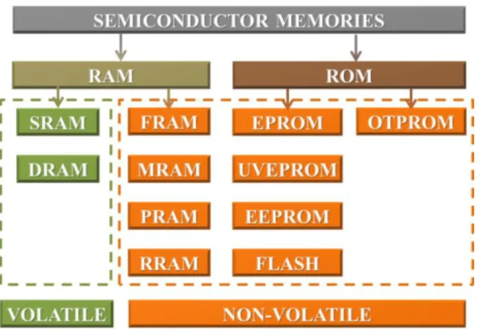
Semiconductor memories can be subdivided into two subcategories based on the ability to rewrite information, e.g. Random Access Memories (RAM) and Read Only Memories (ROM). In contrast to ROMs, in RAMs the information can be written to or read from any cells without read/write cycle limitations. Figure 1.1 illustrates the semiconductor memories explained in this section.
Chapter 1 - Introduction
3
In RAMs the writing and reading times are about the same, whereas in ROMs writing takes more time than reading. In ROMs stored information remains even if the power is turned off, in other words, it is a NVM. On the other hand RAMs are not able to retain the stored information once the power is turned off which makes them volatile memories. Volatile memories such as DRAMs and SRAMs have very fast operation cycles. SRAMs can write and erase in a time of 0.3 ns and are used as a cache memory. [2] DRAMs are slower, being capable of operating in a range of 10 ns. They are used as main memories where the capacity is critical for temporary information storage and processing. [3] NVMs are characterized by their re-programmability. ROMs are classified as One-Time Programmable ROMs (OTPROMs) or Erasable Programmable ROMs (EPROMs). OTPROMs do not have the ability to be reprogrammable, in other words they are non-erasable. EPROMs can be erased either by exposing memory cells to ultraviolet radiation (Ultraviolet EPROMs: UVEPROMs) in which all cells are erased at the same time, or by electrical means (Electrically Erasable PROMs: EEPROMs) in which a byte can be erased through time.
Research is pursuing small, cheap, fast and reliable technologies. A number of alternatives to DRAMs and flash memories have been extensively studied to obtain more powerful and functional memories, so-called emerging memories (see Figure 1.1). The focus of research in emerging memories is on obtaining non-volatile, fast, high-density, low-power consumption, high data transfer rate and reliable memories. If these emerging memories satisfy the positive points of RAMs and ROMs, then they can be universal future memories.
The economic relevance of this matter has easily reached the billion dollar landing and according to MarketResearch.com report, the global market for emerging NVM is expected to increase to $1.6 billion by 2015 at an average annual growth rate of 69 per cent through the forecast period.
Most of non-volatile memories used today consist of four types: flash memory, Ferro-electric RAM (FRAM), Magnetic (MRAM) and Phase change memory (PRAM). Although these technologies are revealed to be quite promising, the scaling down process is proving to be a challenge. Figure 1.1 illustrates the categories of standard semiconductor memories and emerging memories.
Chapter 1 - Introduction
4
Figure 1.1 - Categories of standard semiconductor memories and emerging memories, e.g. FRAM,
MRAM, PRAM and Resistive random Access memory (RRAM). [4]
1.1.2. Flash memories
Flash memory belongs to the class of EEPROM, and is the most suitable structure of non-volatile memory, since one cell consists of only one transistor. Each memory cell in a flash memory consists of only one metal-oxide semiconductor field-effect-transistor (MOSFET) with an additional floating gate, unlike EEPROMs (two MOSFETs). Charge can be stored in this floating node and determines the state of the memory by changing the threshold voltage of the transistor. The addressing process however is much slower than that of DRAM, although these gates can store their charge for a very long time typically write/erase times of 1 ms and 0.1 ms respectively. Figure 1.2 illustrates the cross section of a floating gate transistor.
Figure 1.2 - Basic scheme (cross section) of a flash memory cell. Depending on the charge stored in the
floating gate one bit Single-Level Cells (SLC) or multiple bits Multi-Level Cells (MLC) can be saved. [5]
The operation of flash is based on a process of removing or putting electrons on the floating gate. Charge on the floating gate affects the threshold of the memory
Chapter 1 - Introduction
5
element. When electrons are present on the floating gate, no current flows through the transistor, indicating logic 0. The transistor is conducting, indicating logic 1, when electrons are removed from the floating gate. The process of forcing electrons to/from the floating gate is achieved by applying a voltage between the control gate and source or drain, e.g. Fowler-Nordheim (F-N) Tunneling.
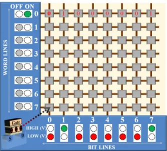
Transistors organized in a chip form a memory array. Figure 1.3 represents the basics of a memory array.
Figure 1.3 - A memory array based on transistors arranged into rows (word lines) and columns (bit lines)
inside a memory chip. The illustration represents a byte of data being written in memory. [6, 7]
Transistors are arranged into rows (word lines) and columns (bit lines) inside a memory chip. To write a byte of data to memory, high voltage is applied to the word line on which the byte appears. Then high voltage is applied to the bit lines where a 1 should appear; low voltage is applied to bit lines where a 0 should appear. An example is given where character "A" is stored in the memory by applying voltage so that the binary value 01000001 is represented across a word line. With availability of megabytes (millions of bytes) of memory, sequences of word lines are combined to represent words, sentences, paragraphs and other combinations of alphabetic, numeric and special characters.
The demands of technology necessitate the scaling of flash devices which is becoming harder to achieve in a reliable way due to the limitations of current lithography technology. The operation speed of flash memory is still slow, compared to
Chapter 1 - Introduction
6
volatile memory. The fastest programming times are in the range of μs (also depending on what kind of tunnel process is used) and the erase times are in the ms range. Additionally, although flash memories function well for the typical 5 V operation, there is an international agreement within the electronics industry that the standard Si-logic level will decrease from 5 V to 3.3 V to 1.1 V and eventually to 0.5 V in the coming years. This might represent a significant bottleneck for flash memories once they are based on Fowler-Nordheim tunnelling. Eventually, reliability could become a serious concern at low voltages such as 0.5 V.
In order to satisfy the previously discussed obstacles, a new hope has arisen. Memristor (memory resistor) devices [1] have given hope to semiconductor companies by offering an easier way to increase the storage density by using current fabrication technology. The device is a resistance that maintains a functional relationship between the time integrals of current and voltage. A memristor consists of a two-terminal device whose resistance depends on the magnitude, polarity and length of time of the voltage applied to it. When the voltage is turned off, the resistance remains as it did just before it was turned off. This makes the memristor a non-linear, nonvolatile memory device. In 1971 memristor was defined by Chua [1] as the fourth fundamental circuit element. In 2008, Hewlett-Packard (HP) Labs [8] presented the first experimental realization as well as a theoretical model of memristor. Current fabrication infrastructures warmly welcome a technology that requires even less wafer space which also reduces the complexity of circuit interconnections, and facilitates high density integration when used in crossbar structures. Furthermore, these devices do not suffer any drawback in relation to the quality and reliability of the tunnel oxide. Thus, it is expected that memristor devices will overtake flash memory in speed, scalability and durability.
1.2. Resistive switching
1.2.1. Resistive switching
Resistive switching can exhibit two or more different resistance states referred to in the simplest case as High Resistance State (HRS) and Low Resistance State (LRS). The resistance states are non-volatile and can be toggled by simply exceeding threshold voltages Vth, SET or Vth, RESET. The digital information like ‘‘0” can be defined by LRS and ‘‘1” by HRS. The information is retrieved by measuring the electrical current,
Chapter 1 - Introduction
7
when a small read voltage Vread is applied. In addition intermediate states in LRS and HRS might be used to store more than one bit per cell. [9] Typically this type of element is a Metal Insulator Metal (MIM) structure (see Figure 1.4(a)) that can be incorporated into cross-point arrays (see Figure 1.4(b)), provided that it exhibits sufficient rectification or other nonlinear response.
Figure 1.4 – (a) Diagram of a RRAM memory cell with a capacitor-like structure in which an insulating
or semiconducting oxide is sandwiched between two metal electrodes. (b) Diagram of a cross-point memory structure. Word and bit lines are used for selecting a memory cell and writing/reading data, respectively.[10-12]
The concept of resistive switching cells deals with two terminal devices instead of three terminal devices as in DRAM where always one access transistor is used. This of course offers the opportunity for novel and advanced architectures. [13, 14]
1.2.2. Categories of resistive switching
Resistive Random Access memory (RRAM) is typically a simple capacitive structure whose resistance can be programmed reversibly by a voltage pulse to be high or low. Once switched, the memory cell retains the particular resistance level for a long time. Devices incorporating switchable resistive materials are generically classified as RRAM. There are numerous variations, few of which have clearly identified mechanisms of conductance and switching. In 1962, Hickmott [15] first reported hysteretic current density–voltage (JV) characteristics in metal-insulator-metal (MIM) structures of Al/Al2O3/Al, indicating that resistive switching occurs as a result of
applied electric fields. Thus, RRAM devices show switching between a low current (OFF) state and a high-current (ON) state as illustrated in Figure 1.5.
Chapter 1 - Introduction
8
Figure 1.5 – Current -Voltage (I-V) characteristics in the Low Resistive State and High Resistive State of
a bistable resistive switching diode.
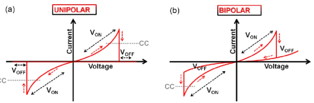
The voltage controlled Negative Differential Resistance (NDR) region consists of a single or possibly a few switching-off events. The memory can be switched between HRS and LRS by applying voltage pulses with amplitudes corresponding to the top and bottom of the NDR respectively. [16-18] When the LRS current is highly localized to a small fraction of the device area, one has a phenomenon generally named “filamentary” conduction. [19-22]
Usually, resistive switching mechanisms can be classified as unipolar and bipolar switching. Unipolar switching depends only on the amplitude of the applied input (voltage/current), whereas bipolar switching depends on both amplitude and polarity. Unipolar switching means that switching-on and switching-off takes place with the same polarity e.g. either negative or positive (Figure 1.6(a)). Thereby the switching-on operation is limited with a current compliance as illustrated in Figure 1.6(b), the transition from HRS to LRS takes place with one polarity and the switching-off with the opposite polarity.
Figure 1.6 – Typical unipolar type of switching curve of a RRAM device. (b) Bipolar type of switching
characteristics. In unipolar switching, the switching direction depends on the amplitude of the applied voltage. Bipolar switching shows directional resistance switching according to the polarity of the applied voltage. [12]
Chapter 1 - Introduction
9
1.2.3. Materials for RRAMs
Resistive switching effect has been observed in a variety of materials, including perovskite oxide materials such as Pr1−xCaxMnO3 and Cr-doped SrZrO3, [9, 23] binary
oxides such as NiO [24] ZnO [25] and ZrO2, [26] chalcogenides,[27] NiO, Nb2O5, Al2O3, SiOx, TiO2, [16, 28-33] organic materials, [34] and amorphous silicon. [35]
Bozano et al. published a complete review of these non-volatile memory elements based on organic materials. [36] Already in 1970, switching in various polymers [37, 38] such as polystyrene, polyacetylene and polyaniline [39, 40] was observed. In semiconducting
polymers such as poly(vinylcarbazole), [41] poly(thiophene), [42, 43]
poly(spirofluorene) [21] and poly(phenylene vinylene) [44] similar switching was observed. Furthermore, switching has also been reported in small molecule semiconductors, such as anthracene, [45] pentacene, [46] Alq3, [47, 48] TPD, [49]
AIDCN, [50] incorporated in MIM diodes. Copper tetracyanoquinodimethane (CuTCNQ) has also been studied. [51-53] For some π-conjugated polymer films that are doped with inorganic salts, memory effects have been reported. [54-56] For this particular class of polymer films, the effects can be interpreted in terms of movement of inorganic ions, a notion that is supported by the observation of relatively gradual changes in conductivity. Another type of conjugated polymer memories, for which a mechanistic explanation of the switching has been established are the polymer fuses. [57] Here the conductivity displayed by conducting polymers (e.g. PEDOT:PSS, polyaniline) can be reduced irreversibly via chemical degradation as a result of Joule heating. These memories classify as Write Once Read Many (WORM). [58] Finally, memory effects have also been reproduced through the inclusion of nanoparticles of different types, like Al nanoparticles [17, 59] or Au nanoparticles [60-64] and the incorporation of a metal inter layer sandwiched between organic or polymeric layers. [64-66]
1.3. Resistive switching models
Up to now, a few models for the driving mechanism of resistive switching have
been proposed, [67-71] e.g., thermochemical, oxygen vacancy migration,
Chapter 1 - Introduction
10
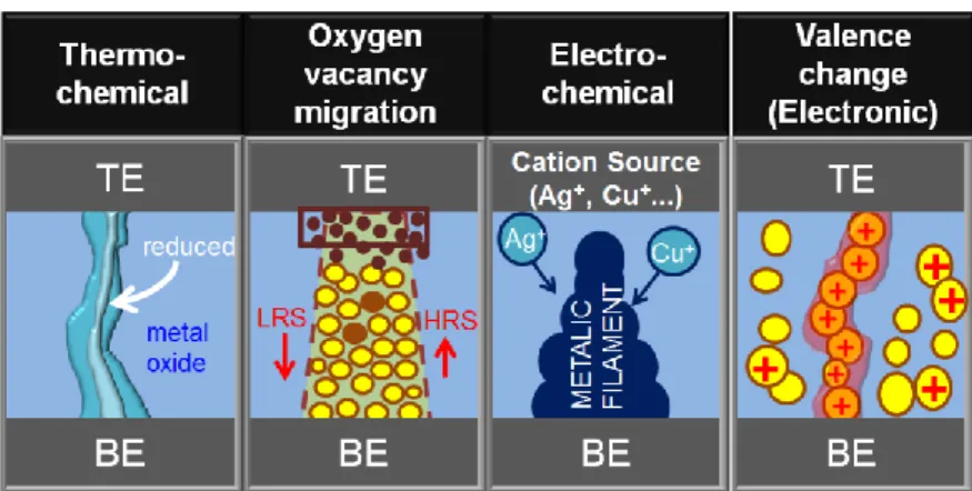
Figure 1.7 - Classification of resistive switching mechanisms in Meal-Insulator-Metal (MIM) structures
between Bottom Electrode (BE) and Top Electrode (TE). [72]
The thermochemical mechanism is known as the fuse-anti-fuse type. Applied voltage induces partial breakdown of the switching material, which puts the system in a low resistance state. Then, the filament type conductive path is disrupted by Joule heating which is caused by the high current density through the conductive filament [12] as illustrated in Figure 1.7(a). A typical resistive switching based on a thermal effect shows unipolar characteristics. It is initiated by a voltage-induced partial dielectric breakdown in which the material in a discharge filament is significantly modified due to Joule heating. Due to the current compliance, only a weak conductive filament with a controlled resistance is formed. This filament may be composed of the electrode metal transported into the insulator, carbon from residual organics, [20] or decomposed insulator material such as sub-oxides. [73] The filamentary nature of the conductive path in the LRS has been confirmed (for NiO [74] and TiO2 [75]). Pt/NiO/Pt thin film based cells have been successfully integrated into CMOS technology to demonstrate non-volatile memory operation. [76] A critical parameter for this unipolar switching effect seems to be the value of the current compliance. In fact, it has been shown that a TiO2 thin film exhibits bipolar switching, and, on setting the current compliance to a larger value, can be turned into a unipolar switching characteristic. [77]
Oxygen vacancy migration mechanisms depend on binary oxide-based resistive memory structures [78] and the ability of some metals to get oxygen atoms from the rich oxide over layers. A good example is the Ti/HfOx/Pt device. When a positive bias is applied on the TE, oxygen vacancies are driven towards the bottom interface (HfOx/Pt) under electrical stimulus. [79] Inhomogeneous migration of oxygen vacancies would lead to the local formation of oxygen-deficient conducting channels [80-82] e.g. LRS. Once a negative bias is applied on the TE, the oxygen vacancies are forced
Chapter 1 - Introduction
11
backwards and gathered near the Ti TE/HfOx interface. The device is therefore switched back to HRS due to the rupture of the oxygen-deficient conducting channel at the HfOx/Pt interface. [83]
The electrochemical mechanism is based on an electrode made from an electrochemically active electrode metal, such as Ag or Cu, an electrochemically inert counter electrode, such as Pt, Ir, W, or Au, and a thin film of a solid electrolyte sandwiched between both electrodes. [84] Using Cu as the active electrode (anode) and Pt as the counter electrode (cathode) metal: [84, 85] (i) anodic dissolution of Cu; (ii) drift of the Cu cations across the solid-electrolyte film under the high electric field; (iii) reduction and crystallization of Cu on the counter electrode surface. The electro-crystallization process leads to the formation of a metal filament. After the filament has grown sufficiently far to make a contact to the opposite Cu electrode, the cell has switched to the LRS. (iv) A sufficient voltage of opposite polarity is applied and the electrochemical dissolution of the metal filament switches the cell to its initial HRS.
Valence change phenomena consist of a considerable generic class of the resistive switching mechanisms. Thus a few relevant mechanisms are discussed. Many binary transition metal-oxides as well as multinary oxides with at least one transition metal sublattice show bipolar resistive switching even though the electrodes do not inject metal cations. This missing cation injection may be either because the electrode metal is not easily oxidized (in the case of Pt, Au, etc.) or the oxidized form is not easily reduced back to the metal (in the case of Al, Ti, Nb, etc.). First reports which seem to fall into this category go back to the 1960s when Nb/NbOx thin film cells were studied. [86] In
the late 1990s, Tokura, Kawasaki and their colleagues started to study bipolar resistive switching phenomena for various manganites [87, 88] while Bednorz and his colleagues focused on titanates and zirconates. [9, 89] Similarly to the electrochemical metallization cells, usually an electroforming step is required before bistable switching is achieved. Often, the electroforming is a somewhat slower process (milliseconds to thousands of seconds), than the actual switching depending on the geometry of the system (thin film MIM structures, lateral MIM cells, single crystals) and the electroforming parameters. The polarity of the bipolar switching cycle is not always obvious. It seems to be determined by many factors such as the work function and the oxygen affinity of the electrode metals, in particular, if different metals are used for the two electrodes of a cell, the polarity of the electroforming process, the formation of
Chapter 1 - Introduction
12
interface layers, etc. [84] A major contribution of this type of resistive switching mechanism falls into a so called electronic view. There are several conceivable mechanisms that lead to a resistance change of the system by purely electronic effects. One possibility is the charge-trap model, [16] in which charges are injected by Fowler– Nordheim tunnelling at high electric fields and become subsequently trapped at sites such as defects or metal nanoparticles within the insulator. This modifies the electrostatic barrier character of the MIM structure and, hence, the resistance of the structure, resembling the gate–channel resistance in Flash FET. For example, metal nano-clusters incorporated in either polymeric [60, 62] or inorganic insulator films [90] are reported as trapping sites. In contrast to the purely electronic switching models, a large body of literature has built up during recent years in which the participation of a transport of anions is considered essential for resistance switching. In many transition metal-oxides, oxygen ion related defects, typically oxygen vacancies, are much more mobile than the transition metal cations. Enrichment or a depletion of oxygen vacancies will affect the valence state of the transition metal cations and may lead to a considerable change in electronic conductivity. [84]
1.4. Aim of the thesis
Resistive switching memories are being investigated due to their huge potential application for data storage. The mechanism is still not well understood. The objective of this thesis is to understand the switching mechanism and to quantitatively explain the switching dynamics.
The thesis is organized as follows. In Chapter 2 the metal-oxide polymer diodes are analysed as a bi-layer structure. A physical model that describes the current-voltage characteristics of the bi-layer is derived. This model is then translated into a simpler and conveniently equivalent circuit that consists of the series-parallel combination of resistors and capacitors. The dynamic behaviour of this equivalent circuit was simulated for both conduction states using triangular voltage profiles with different scan rates. The results were used later to compare with the experimental results and disentangle the effects caused by the resistive switching process.
In Chapter 3 the dynamic response of the non-volatile bistable resistive memory was studied in both the HRS and LRS, using triangular and step voltage profiles. The
Chapter 1 - Introduction
13
results provide insight into the wide spread in switching times reported in the literature and explain an apparently anomalous behaviour of the LRS, namely the disappearance of the negative differential resistance region at high voltage scan rates which is commonly attributed to a “dead time” phenomenon. The HRS response follows closely the predictions based on a classical, two-layer capacitor description of the device. The fundamental limitations on the speed of operation of a bi-layer resistive memory are reviewed and explained.
In Chapter 4, the current–voltage characteristics of RRAM are studied as a function of temperature. Findings indicate that creation and annihilation of filaments is controlled by the filling of shallow traps localized in the oxide or at the oxide/polymer interface.
Low-frequency noise is studied in resistive-switching memories based on metal– oxide polymer diodes in Chapter 5. The noise spectral power follows a 1/fγ behaviour, with γ = 1 in the ohmic region and with γ = 3/2 at high bias beyond the ohmic region. The exponent γ=3/2 is explained as noise caused by Brownian motion or diffusion of defects which induce fluctuations in diode current. Evidence that the noise is generated in narrow localized regions in the polymer between the contacts is provided.
In Chapter 6, a study on random telegraph noise (RTN) current fluctuations in RRAM devices is presented. The influence of temperature and electric field on the RTN fluctuations is studied in different conductance states to reveal the dynamics of the underlying fluctuators.
In Chapter 7 a diagnostic tool for Organic Light Emitting Diode (OLED) reliability is proposed. The work addresses the early degradation problem using small-signal impedance measurements and electrical noise techniques. It is proposed that a combination of both measurements can be used as a diagnostic tool for OLED reliability.
Chapter 8 describes non intentional resistive switching in other systems. A relation between OLED degradation and resistive switching is discussed. Evidence of trapping mechanisms occurring in the OLED is provided by small-signal impedance results and the observation of optical bursts of higher wavelength than the band-gap electroluminescence. The nature of the trap responsible for resistive switching is suggested based on temperature measurements.
Chapter 1 - Introduction
14
In conclusion, this thesis presents a detailed electrical characterization of the resistive switching mechanism in metal-oxide polymer memories. Resistive switching was also studied in small-molecule OLEDs. It was shown that the degradation that leads to a loss of light output under operation is caused by the presence of a resistive switching layer. A diagnostic tool that predicts premature failure of OLEDs was devised and proposed.
Chapter 2 - An equivalent circuit model for a metal-oxide polymer diode
15
An equivalent circuit model for a
metal-oxide polymer diode
Metal-oxide polymer diodes are analysed as a bi-layer structure. A physical model that describes the current-voltage characteristics of the bi-layer is derived. This model is then translated into a simpler and more convenient equivalent circuit that consists of the series-parallel combination of resistors and capacitors. The dynamic behaviour under voltages ramps was simulated for both conduction states; the frequency dependence of the admittance was also simulated. The results were used later in this thesis to compare with the experimental behaviour and disentangle the effects caused by the resistive switching process.
Chapter 2 - An equivalent circuit model for a metal-oxide polymer diode
16
2. An equivalent circuit model for a metal-oxide polymer diode
2.1. Introduction
This chapter presents an equivalent circuit model for the internal capacitive bi-layer structure of metal-oxide polymer memories. A comprehensive analysis of the equivalent circuit response to varying voltages ramps speeds for both conduction states was carried-out. The model predicts the electrical behaviour for both high and low resistance states. The estimated time constants provide insight about which transitions (from high to low resistance or from low to high resistance) control the programming speed of these types of memories. The frequency response of the diode is also derived. It is shown that if the polymer is conductive enough, the bi-layer exhibits a Maxwell-Wagner type of relaxation.
2.2. Device physical structure and equivalent circuit model
The physical model treats the diode as a bi-layer with different conductivity and permittivity as well as different physical dimensions (see Figure 2.1). It also assumes that a space charge layer exists at the interface between the two layers. Although this is only an assumption, clear experimental evidences for this fixed space charge will be provided later in Chapter 3. The differential equation for the current across the bi-layer system is derived. The physical system can be described as a simple equivalent circuit if the physical parameters in the differential equation are replaced by resistances and capacitances. The frequency dependence admittance of the diode is also interpreted using this double RC equivalent network.
Chapter 2 - An equivalent circuit model for a metal-oxide polymer diode
17 Aluminium oxide-polymer capacitors can be modeled as a two dieletric conductive layers as shown in Figure 2.2.
Figure 2.2 – Schematic representation of two dielectric conductive layers in series as a model for the
metal-oxide polymer diode.
In Figure 2.2 the device is represented by two dielectric conductive layers, the oxide and the polymer layer, sandwiched between the electrodes and characterized by their thicknesses LOX and LPOLY the electric permittivity’s OX and POLY, and electric conductivities, gOX and gPOLY respectively. The applied voltage is given by equation (2.1):
(t)= O (t)LO OL (t)L OL = O (t) OL (t (2.1) Being O (t and OL (t the corresponding voltage drop across the oxide and the polymer layer respectively.
The current density across the device is given by equation (2.2):
(t)=g OL OL (t) OL
d OL (t
dt =gO O (t) O
d O (t
dt (2.2)
A small current may flow across the two layers. This causes the appearance of a charge density at the interface between the layers as given by equation (2.3):
σ(t)= O O OL OL (2.3)
This set of equations can be solved allowing us to obtain the dependence of ( ), ( ) and ( ) on the applied voltage V(t). The differential equation for ( ) is given by equation (2.4):
Chapter 2 - An equivalent circuit model for a metal-oxide polymer diode 18 ( OL O L OL LO )d OL (t dt (g OL gO L OL LO ) OL (t)=gO LO (t) O LO d (t) dt (2.4) and can be analytically solved.
The permittivity’s and conductivities can be replaced by the resistances, RO = Lg O O and R OL = L OL g OL , and capacitances, O = O LO and = OL L OL . The differential equation for ( ) is described in equation (2.5):
d OL (t dt R RO R OL OL (t = 1 [ (t) RO ox d (t) dt ] (2.5) Where = OL O and R=R OL RO .
By analysing the above equations, written in terms of capacitances and resistances, one can recognize that the two conductive dielectric layers are equivalent to two parallel RC circuits connected in series as given by Figure 2.3.
Figure 2.3 - The equivalent circuit used for modelling the bi-layer structure.
Assuming a ramp voltage as ( ) where k is the ramp speed, the expression for the ( ) can be derived as shown in equation (2.6):
( ) ( ⁄ ) (2.6)
Where B=R OL RO
R ( ox- R OL
Chapter 2 - An equivalent circuit model for a metal-oxide polymer diode
19 The time constant for the device to be charged or discharged is . The electric current, I(t), trough the device can be readily calculated using the equation (2.2) as follows: (t)= OL (t) R OL OL d OL (t) dt = =k( B R OL R OL OL R ) k Rt kB( OL 1 R OL ) e t ⁄ (2.7)
2.2.1. Limits for the RRAM in LRS and HRS
The HRS with O OL and RO R OL leads to a time constant for the device of R OL O . In this limit the electric current is described through equation (2.8): (t) k ( O t RO O e t ⁄) = (t RO k O (1 e t ⁄ (2.8)
Similarly, the LRS O OL and R R lead to R O . In this limit, the electric current is given by equation (2.9):
(t) k( OL t
R OL =k OL
(t
R OL (2.9)
The expressions above shows that the electric behaviour for the device in HRS is governed essentially by O and , while the LRS is dependent of and OL .
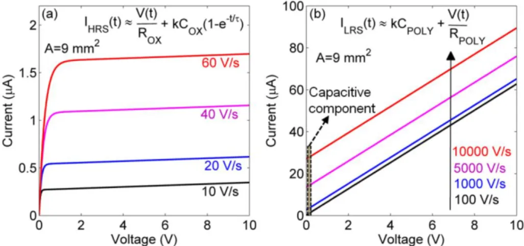
The dependence of the current on the applied voltage, at several ramp speeds (equations 9 and 10) and in both resistive states are given in Figure 2.4(a) and Figure 2.4(b).
Chapter 2 - An equivalent circuit model for a metal-oxide polymer diode
20
Figure 2.4 - Theoretical IV characteristics of an Al2O3/polyspirofluorene (PFO) bistable resistive
switching diode obtained (a) in the HRS for different voltage sweep rates (b) obtained in the LRS for different voltage sweep rates.
Figure 2.4(a) shows the experimental JV characteristics for the HRS obtained with increasing voltage scan speeds. The HRS was considered with O OL and RO R OL . Meanwhile, the LRS is based on O OL and R RO . Equation (2.8) is represented in Figure 2.4(a) with a voltage sweeps of 10 V/s, 20 V/s, 40 V/s and 60 V/s. A dynamic behaviour of a parallel plate capacitor is observed. The current increases due to the effect of the displacement current density (t)= O d dt⁄ , where O is the oxide capacitance per unit area. The current voltage characteristics in the LRS are shown in Figure 2.4(b). A capacitive component of the RC structure is represented in dash lines. The current response in Figure 2.4(b) relates to equation (2.9). The current increases linearly as higher ramp rates are applied. The internal device structure is basically a voltage divider. Since the oxide capacitance is much larger than the polymer capacitance, the voltage division of the applied external bias must depend on the voltage scan speed.
2.2.2. The time constants
The time constant for the device in HRS state is larger compared to the time constant for LRS state since off R OL O and on RO O , i.e., off on. In the HRS state using values O =2 nF and R OL =1 0 k , we get off= ms. In the LRS state using values O =2 nF and RO = 0 k , we get on= ms. This agrees with the fact that the device can switch faster from the LRS to HRS than for the HRS to LRS
Chapter 2 - An equivalent circuit model for a metal-oxide polymer diode
21 state. [91] This analysis is important for the diode optimization (in terms of physical dimensions) to achieve the highest switching speed.
2.2.3. The frequency dependence admittance of the diode
The equivalent circuit is also used to explain the frequency dependence admittance of the diode. The simulated frequency dependence of the capacitance and dielectric loss (G/ω) where G is the conductance and ω=2πf of the double RC network is shown in Figure 2.5.
Figure 2.5 – Theoretical representation for the RRAM structure using the equivalent circuit represented
in Figure 3. The parameters used are according to the geometrical capacitances as in [92] e.g. ROX= MΩ,
COX=27 nF, RPOLY=10 KΩ, POLY=2.7 nF.
In Figure 2.5, the capacitance (C) and loss (G/ω) for a conducting RRAM device is presented. As frequency increases, the capacitance varies between the oxide geometric capacitance to the series capacitance of the oxide and polymer. A high loss at low frequencies which rises as 1/f for a dc resistance is illustrated. The changes in the device are purely resistive. For conducting illustration purposes ROX was set to MΩ representing the LRS. The dispersion centred on 500 kHz is typical of the Maxwell– Wagner relaxation process [93] observed in two-layer dielectric structures and can be modelled by the double RC circuit represented in Figure 2.3. The dispersion in capacitance centred at frequency fR is given by equation (2.10):
Chapter 2 - An equivalent circuit model for a metal-oxide polymer diode 22 fR= 1 R⁄ 1 R⁄ 2π( ) (2.10)
Which for R R reduces to: fR=
1
2πR ( )
(2.11)
At low frequencies the capacitance is dominated by the oxide capacitance. Above, in equation (2.11) the relaxation frequency the measured capacitance corresponds to the series sum of COX and CPOLY, therefore dominated by CPOLY.
2.3. Conclusion
Metal-oxide polymer diodes have been analysed as a bi-layer structure and a physical model that describes the current-voltage characteristics of the bi-layer derived. The dynamic response upon voltage ramps reveals that HRS behaves as a classical parallel plate capacitor. The LRS is ohmic. However, there is a voltage division effect due to the internal bi-layer. The electrical behaviour upon changing voltage ramp speed was calculated for both states. The findings show that the time constants of both states are very different; the time constant associated to the HRS is much longer than the time constant of the LRS. This difference in time constants causes the switch from a high to a low resistance state to take longer than a switch from a low to a high resistance state.
Provided that the polymer layer is conductive, a Maxwell-Wagner dispersion is expected to be observed in the frequency window [20 Hz-1MHz].
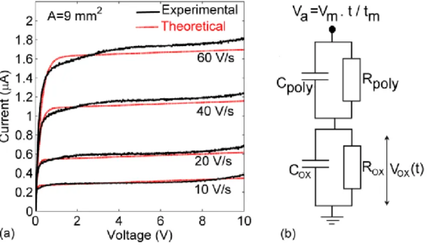
Chapter 3 will present the experimental HRS and LRS behaviour upon the input of high speed triangular profiles. Furthermore, a comparison between the calculated and experimental result will be described and the importance of the bi-layer structure in the resistive switching process enlightened.
Chapter 3 - The role of internal structure in the anomalous switching of RRAMs
23
The role of internal structure in the
anomalous switching dynamics of
metal-oxide polymer resistive
RAMs
The dynamic response of a non-volatile, bistable resistive memory fabricated in the form of Al2O3/polymer diodes has been probed in both the HRS and LRS using triangular and step voltage profiles. The results provide insight into the wide spread in switching times reported in the literature and explain an apparently anomalous behaviour of the LRS, namely the disappearance of the negative differential resistance region at high voltage scan rates which is commonly attributed to a “dead time” phenomenon. The HRS response follows closely the predictions based on a classical, two-layer capacitor description of the device. As voltage scan rates increase, the model predicts that the fraction of the applied voltage, Vox, appearing across the oxide decreases. Device responses to step voltages in both the HRS and LRS show that switching events are characterized by a delay time. Coupling such delays to the lower values of Vox attained during fast scan rates, the anomalous observation in the LRS that, device currents decrease with increasing voltage scan rate, is readily explained. Assuming that a critical current is required to turn off a conducting channel in the oxide, a tentative model is suggested to explain the shift in the onset of negative differential resistance to lower voltages as the voltage scan rate increases. The findings also suggest that the fundamental limitations on the speed of operation of a bi-layer resistive memory are the time- and voltage-dependences of the switch-on mechanism and not the switch-off process.