PROCEEDINGS OF SPIE
SPIEDigitalLibrary.org/conference-proceedings-of-spie
Resonant tunnelling diode based
high speed optoelectronic
transmitters
Jue Wang, G. C. Rodrigues, Abdullah Al-Khalidi, José M.
L. Figueiredo, Edward Wasige
Resonant Tunnelling Diode Based High Speed Optoelectronic
Transmitters
Jue Wang
a, G. C. Rodrigues
b, Abdullah Al-Khalidi
a, José M. L. Figueiredo
band Edward Wasige
aa
School of Engineering, University of Glasgow, Oakfield Avenue, Glasgow, G12 8LT, UK.
b
Departamento de Fisica, Universidade do Algarve, Campus de Gambelas, 8005-139 Faro, Portugal.
ABSTRACT
Resonant tunneling diode (RTD) integration with photo detector (PD) from epi-layer design shows great potential for combining terahertz (THz) RTD electronic source with high speed optical modulation. With an optimized layer structure, the RTD-PD presented in the paper shows high stationary responsivity of 5 A/W at 1310 nm wavelength. High power microwave/mm-wave RTD-PD optoelectronic oscillators are proposed. The circuitry employs two RTD-PD devices in parallel. The oscillation frequencies range from 20-44 GHz with maximum attainable power about 1 mW at 34/37/44GHz.
Keywords: resonant tunneling diode, photo diode, oscillator, photodetector
1. INTRODUCTION
As the demand for high speed wireless communication continues to increase exponentially, the need to utilize the high speed optic fiber which has been widely employed in most base stations for wireless broadband communications is higher than before. The resonant tunnelling diode photodetector (RTD-PD) technique can provide a low cost solution for the seamless integration of microwave/mm wave radio and fiber networks.
Resonant tunneling diode is considered to be the fastest solid-state electronic device. To date, the highest reported frequency of RTD oscillator is 1.92 THz [1]. To benefit from the RTDs’ capability of high frequency sources, the monolithically integration of a light sensitive layer-photo detector was introduced with RTD epi-layer design. RTD based photo-detector shows great potential applications for optical-electrical modulation and photo-detection [3]. Optimization of RTD-PD layer structures to maximize the sensitivity and responsivity is one of the key factors for real applications. Another key factor is high power/high frequency RTD-PD oscillator design. 30 Gbps wireless communication over a few centimeters distance has been demonstrated by using electrical-only modulated RTD oscillator at 500 GHz [2]. The short distance is mostly due to low output power which was in tens of microwatt range. Different from most RTD relaxation oscillator design [4][5], the proposed RTD-PD LC oscillator circuit utilize two RTD-PDs in parallel. Each device was biased individually to suppress the parasitic oscillation. Device size was also optimized in terms to provide best impedance matching. 1mW output power RTD-PD oscillators are reported here. It is expected that with improved device epi-layer design and oscillator output power level, RTD-PD technology can be widely utilized in the long distance/ ultra-high speed optical-wireless communication system.
2. RTD-PD LAYER STRUCTURE
As RTD devices exhibit negative differential conductance (NDC) gain over extra wide bandwidth, the RTD-PD device would act as optical receiver with a build in amplifier, which can extract from the optical modulated signal to the RF carriers and amplify it by using RTD as high frequency sources [3][6]. The typical RTD device layer structure consists of a narrow band gap - quantum well material sandwiched between two wide band gap-double barrier materials, namely double barrier quantum well (DBQW) structure. A RTD-PD structure integrates the DBQW within the photo-conductive layers as shown in Table 1, that InGaAs/AlAs RTD was monolithically integrated with 500 nm photo absorption layer- InGaAlAs on top of DBQW. The RTD-PD device is optimized to maximize the optical response, namely the responsivity and sensitivity. Responsivity is a critical parameter to determine the max output saturation power while sensitivity determines the lowest detectable power. The RTD-PD stationary state responsivity
( V
,
)
at bias voltageV
is definedby hc e V M P V I V I V ph light dark light DC ( ) ) ( ) ( ) ( ) , (
Where
I
light(V
)
is the current illumination andI
dark(V
)
is the current under dark conditions,P
light
is the incident optical power,
is the wavelength of the incident light wave, M(V) accounts for the internal current gain effect (due to electron-holes generation and/or impact ionization mechanisms),
ph is the external quantum efficiency; e ,h
and c are the elementary charge, the Planck constant and the speed of light in the vacuum, respectively. The built-in gain factor) (V
M accounts for the internal current gain effect (due to the photo-generated electron-holes pairs and impact ionization mechanisms). Ideally every photo produces one pair of electron-hole, which contribute to photo current without any loss, the quantum efficiency is equal to one and the ideal responsivity would be given simply by
hc e
i
. The ideal maximum responsivity for wavelength 1310 nm and 1550 nm is 1.05 A/W and 1.25 A/W. In reality, many factors reduce the ideal responsivity value such as limited optical absorption efficient, finite absorption layer thickness (penetration depth), and optical reflection at the semiconductor surface, losses due to carrier recombination, and also the detector bandwidth limitation. The frequency response of the RTD-PD is not presented in the paper.
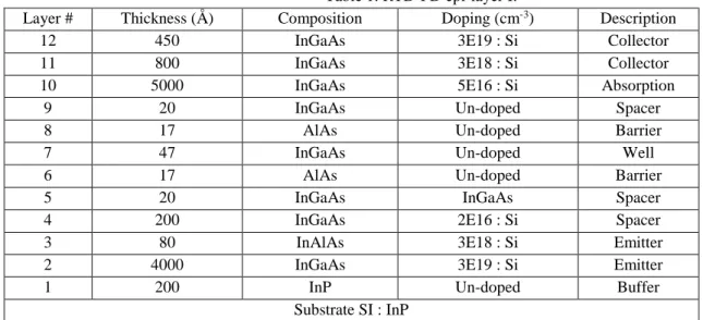
Table 1. RTD-PD epi-layer I.
Layer # Thickness (Å) Composition Doping (cm-3) Description
12 450 InGaAs 3E19 : Si Collector 11 800 InGaAs 3E18 : Si Collector 10 5000 InGaAs 5E16 : Si Absorption
9 20 InGaAs Un-doped Spacer 8 17 AlAs Un-doped Barrier 7 47 InGaAs Un-doped Well 6 17 AlAs Un-doped Barrier 5 20 InGaAs InGaAs Spacer 4 200 InGaAs 2E16 : Si Spacer 3 80 InAlAs 3E18 : Si Emitter 2 4000 InGaAs 3E19 : Si Emitter 1 200 InP Un-doped Buffer
Substrate SI : InP
2.1 DC characteristics
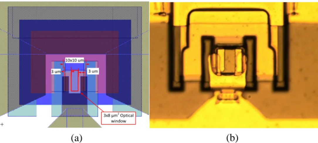
In this paper, 10×10 µm2 sized RTD-PD are investigated. The central optical window is rectangular shape. As shown in
Fig 1 (a), the optical window is 3×8 µm2 for the device design while Fig 1 (b) shows the fabricated device with
clear-opened optical window. The I-V characteristics under dark and light illumination are compared in Fig 2. Under dark condition, the device shows negative differential conductance (NDC) region between 1.1V-1.4V. The peak current density was about 0.3mA/um2, peak to valley current ratio (PVCR) was about 1.5. The device stationary optical response was
investigated with non-modulated continuous wave (CW) light at 1310 nm and 1550 nm. The measurement work was done at Universidade do Algarve. The measurement setup is shown in the inset of Fig 2. The RTD-PD was biased from left (probe). The cleaved single mode optical fiber was aligned with the optical window from device top mesa. The light with wavelength 1310 nm and 1550 nm was coupled into the RTD-PD with 0.1mW and 1 mW power. As shown in Fig 2. (a), the optical DC response of 1310 nm laser with different optical power are compared with dark current. The maximum response was about 5 A/W when RTD-PD was biased close to the peak voltage and the injected light power was 1 mW. As shown in Fig 2. (b), the maximum responsivity of 1550 nm (1 mW) was about 2 A/W. The main difference is due to high absorption efficiency at 1310nm wavelength.
40 35 -30 E 1:3 >D Ú20 415 p10 5 0 0 91 0.2 0.3 0.4 0.5 0.8 0.7 0.8 0.9 1.0 1.1 1.2 1.3 1.4 1.5 1.6 1.7 18 RTDPD Voltage (V)
RTDPDresponse to 1310 nm light (RTD-PD, MO FV Curves)
i i i -dark -0.1 mW opecal power_ 1mW optical power 40 35
FITDPD response to 1550 nm light (RTIRD, A36 1.11 Curves)
-93 E 20 o 15 o I OC 10L -OA -0.1 mW opOcal powef 1 rdll op6cal paver o0 0.1 0.2 0.3 0.4 0.5 0.6 0.7 0.8 0.9 1.0 1.1 1.2 13 1.4 1$ 1.6 11 1.6 FITO-P0 Voltage f1.1) 10x10 um 3 um 3 um 3x8 µm2 Optical window
Figure 1. (a) RTD-PD layout design. The device size was 10×10 µm2, the optical window size was 3×8 µm2. (b) The
micrograph of the top-view of the fabricated device. The optical window is clearly noted.
Figure 2. RTD-PD stationary optical response with light injection power of 0.1 mW and 1 mW (a) The optical response of 1310 nm wavelength. (b) The optical response of 1550 nm wavelength. The device shows large responsivity of 5 A/W for 1310 nm compared to 1550 nm due to high absorption efficiency. Inset shows the measurement setup. The device was biased from left (probe). The injected light was coupled from the top side.
3. RTD-PD OSCILLATORS
High frequency RTD-PD oscillator design utilized the device described above. New epi-layer structure including double light absorption layer on both side of DBQW as shown in Table 2 are introduced and characterized for the consideration of power performance and better optical control. As shown in Figure 3, two different sized devices, 10×10 µm2, 15×15
µm2 are investigated. The central optical windows are 3×8 µm2 and 5×10 µm2 respectively. The NDC region was between
1.2V-2.4V. The peak current density was about 0.16mA/um2 and peak to valley current ratio (PVCR) was about 2. The
measurement results are summarize in Table 3, where ΔV is the peak-valley voltage difference, ΔI is the peak-valley current difference. The maximum negative difference conductance Gn is given by
3ΔI
2ΔV. The estimated maximum power for
each single device is given by 3
16 ΔVΔI when load conductance is GL=Gn/2 [7][8]. Benefit from large ΔV, these devices
shows potential for higher power oscillator design than the above epi-layer I (Table 1) devices.
(a)
(b)
40 35 30
Q 25
Ec
20 2j
15 10 5 0 ti 100 um2 - - -225 um2 '\
,
. -_ . / /..L/
t
...'.
r
I I 00 0.5 10 1.5 20 Voltage (V) 25 30 3.5Table 2. RTD-PD epi-layer II.
Layer # Thickness (Å) Composition Doping (cm-3) Description
13 1000 InGaAs 3E19 : Si Collector 12 3000 InAlAs 3E18 : Si Collector 11 5000 InGaAlAs 2E16 : Si Absorption 10 20 InGaAlAs Un-doped Spacer
9 17 AlAs Un-doped Barrier 8 57 InGaAs Un-doped Well 7 17 AlAs Un-doped Barrier 6 20 InGaAlAs Un-doped Spacer 5 5000 InGaAlAs 2E16 : Si Absorption 4 3000 InAlAs 3E18 : Si Emitter 3 5000 InGaAs 3E19 : Si Emitter 2 1000 InAlAs Un-doped
1 200 InP Un-doped Buffer Substrate SI : InP
Figure 3. The measured RTD-PD IV characteristics (dark). Two different device size 10×10 µm2 and 15×15 µm2 are
compared. The negative differential resistance region is between 1.2V~2.4V.
Table 3. RTD-PD DC characteristics. Device size (um2) Optical window (um2) ΔV(V) ΔI(mA) G
n (mS) Estimated Power (mW)
100 3x8 1.2 7.4 9.3 1.7 225 5x10 1.2 18.5 23.1 3.5
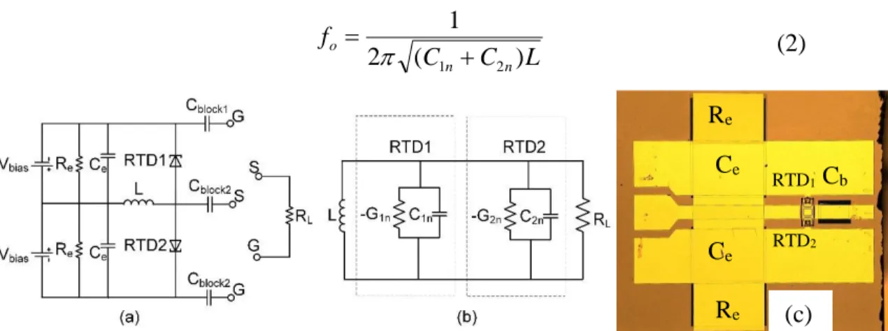
Different from normal RTD-PD relaxation oscillator design [4][5][6] with a single RTD-PD device biased in series with a large inductor (transmission line), the proposed RTD-PD LC oscillator circuit utilize two RTD-PDs in parallel, as shown in Fig. 4(c). Each device is biased individually with shunt resistor to suppress the bias oscillation [9]. The schematic circuit of RTD-PD oscillator is as shown in Fig 4 (a), where Re is the stabilizing resistor, Ce is the bypass capacitor, Cb is the DC
block capacitor, RL is the load. The RF equivalent circuit is shown in Fig 4(b). Each RTD-PD is presented by its negative
Vbias Vbias (a) R L RTD1 RTD2 (b) ,
L
C
C
f
n n o)
(
2
1
2 1
Figure 4. (a) The two RTD oscillator schematic circuit. Each RTD was biased individually with its own DC stabilization circuit Re and Ce. (b) RTD oscillator RF equivalent circuit excluding parasitic elements. (c) Fabricated RTD-PD
oscillator, Re=20 Ω, Ce=60 pF, Cb=7 pF.
The fabricated oscillator photograph is shown in Fig 4 (c). Re is thin film NiCr resistor with Re=20 Ω, Ce/Cb is
metal-insulator-metal (MIM) capacitor with Ce=60 pF, Cb=7 pF. The inductance is introduced by CPW structure. The inductor
value is determined by the CPW length. The design procedure can be found in Ref. [9]. To effectively suppress the parasitic oscillation, Re should satisfy that Re<1/Gn. From the impedance matching point of view, to obtain the maximum power,
the load conductance should satisfy GL= Gn/2. For a 50 Ω load, the optimized device conductance is about 40 mS.
Referring to Table 2, for 225 μm2 single device, G
n=23.1 mS. By utilizing two 225 μm2 RTD-PD device in parallel, the
total conductance is two times larger which is close to 40 mS. In this case, 222 μm2 RTD-PD oscillator provide better
impedance matching, the output power is expected high. The measurement results shown in the following section validate the design.
4. MEASUREMENT RESULTS
The oscillators were characterized on-wafer by using Agilent E4448A spectrum analyzer. A Cascade ACP65 RF probe was used to probe the output of these oscillators. As the cable loss/system loss is not accurately specified by the manufacturer, the actual power loss was characterized by calibrated another signal source Wiltron 68187B. The measurement results are summarized in Table 4. It shows that high frequency RTD-PD oscillators with over 1 mW output power have been developed. The frequency can be further increased by optimize the CPW design. The difference between designed and measured frequency is mostly due to the approximation of the device capacitance.
Table 4. RTD-PD oscillator measurement results. Device size (um2) Optical window (um2) CPW length (μm) Designed Freq(GHz) Measured Freq(GHz) Measured Power (dBm) Calibrated Power (dBm) 100 24 700 30 20.7 -6.7 -1.7 100 24 260 60 34.4 -6.1 0.4 100 24 260 60 37.0 -7.1 0.1 225 50 75 90 44.4 -7.1 +1.4
5.
DISCUSSION AND CONCLUSION
The results presented in the paper show great potential to utilize RTD-PD as high speed optical modulated RF transmitter. The RTD-PD approach to optical/wireless data transmission provides a high efficiency, low cost solution for seamless integration of high speed fiber network with THz wireless communication. The increased power level makes it feasible for long distance applications. More work such as optical injection locking, optical-wireless data transmission, is currently being done with these RTD-PD oscillators.
(2)
(c)
R
eR
eC
eC
eC
b RTD1 RTD2ACKNOWLEDGMENTS
The authors thank the staff of the James Watt Nanofabrication Centre (JWNC) at the University of Glasgow for help in fabricating the devices. This work was supported by European Commission, grant agreement no. 645369 (iBROW project).
REFERENCES
[1] Maekawa, T., Kanaya, H., Suzuki, S., and Asada, M., "Oscillation up to 1.92 THz in resonant tunneling diode by reduced conduction loss," Applied Physics Express, 9(2), 024101 (2016).
[2] Oshima, N., Hashimoto, K., Horikawa, D., Suzuki, S. and Asada, M., "Wireless data transmission of 30 Gbps at a 500-GHz range using resonant-tunneling-diode terahertz oscillator," 2016 IEEE MTT-S International Microwave Symposium (IMS), 1-4(2016).
[3] Figueiredo, J., Romeira, B., Slight, T., and Ironside, C., "Resonant Tunnelling Optoelectronic Circuits,” Advances in Optical and Photonic Devices, InTech. ISBN: 978-953-7619-76-3, (2010).
[4] Chahal, P., Morris, F., and Frazier, G., "50 GHz resonant tunneling diode relaxation oscillator," 62nd Device Research Conference, (1), 241-242 (2004).
[5] Brown, E. R., Parker, C. D., Verghese, S., Geis, M. W., and Harvey, J. F., "Resonant-tunneling transmission-line relaxation oscillator,” Applied Physics Letters, 70 (21), 2787-2789 (1997).
[6] Cantu, H. I., Romeira, B., Kelly, A. E., Ironside, C. N. and Figueiredo, J. M. L., "Resonant Tunneling Diode Optoelectronic Circuits Applications in Radio-Over-Fiber Networks," IEEE Transactions on Microwave Theory and Techniques, 60 (9), 2903-2912 (2012).
[7] Kim, C. S., and Brandli A., "High-Frequency High-Power Operation of Tunnel Diodes,” IRE Transactions on Circuit Theory, 416-525 (1961).
[8] Wang, J., "Monolithic Microwave/millimeterwave integrated circuit resoant tunneling diode sources with around a milliwatt output power, " PhD thesis, University of Glasgow, (2014).
[9] Wang, J., Wang, L., Li, C., Alharbi K., Khalid A., and Wasige, E., "W-band InP-based Resonant Tunnelling Diode Oscillator with Milliwatt Output Power," The 26th International Conference on Indium Phosphide and Related Materials, (2014).