Pawel Jerzy Wojcik
Licenciado em Electrónica
Printable organic and inorganic materials
for flexible electrochemical devices
Dissertação para obtenção do Grau de Doutor em Nanotecnologias e Nanociências
Orientador: Doutora Elvira Maria Correia Fortunato, Professora
Catedrática, Faculdade de Ciências e Tecnologia da
Universidade Nova de Lisboa
Co-orientador: Doutor Rodrigo Ferrão de Paiva Martins, Professor
Catedrático, Faculdade de Ciências e Tecnologia da
Universidade Nova de Lisboa
Júri:
Presidente: Professor Doutor José Júlio Alves Alferes
Arguentes: Prof. Doutora Verónica Cortés de Zea Bermudez
Professor Doutor Albano Augusto Cavaleiro Rodrigues de Carvalho Prof. Doutora Maria Manuela Silva Pires Silva
Vogais: Professor Doutor Rodrigo Ferrão de Paiva Martins
Professora Doutora Elvira Maria Correia Fortunato Prof. Doutor Rogério Manuel dos Santos Simões Prof. Doutor Luís Miguel Nunes Pereira
Doutor Diogo Miguel Franco dos Santos
i
Pawel Jerzy Wojcik
Licenciado em Electrónica
Printable organic and inorganic materials
for flexible electrochemical devices
Dissertação para obtenção do Grau de Doutor em Nanotecnologias e Nanociências
Orientador: Doutora Elvira Maria Correia Fortunato, Professora
Catedrática, Faculdade de Ciências e Tecnologia da
Universidade Nova de Lisboa
Co-orientador: Doutor Rodrigo Ferrão de Paiva Martins, Professor
Catedrático, Faculdade de Ciências e Tecnologia da
Universidade Nova de Lisboa
Júri:
Presidente: Professor Doutor José Júlio Alves Alferes
Arguentes: Prof. Doutora Verónica Cortés de Zea Bermudez
Professor Doutor Albano Augusto Cavaleiro Rodrigues de Carvalho Prof. Doutora Maria Manuela Silva Pires Silva
Vogais: Professor Doutor Rodrigo Ferrão de Paiva Martins
Professora Doutora Elvira Maria Correia Fortunato Prof. Doutor Rogério Manuel dos Santos Simões Prof. Doutor Luís Miguel Nunes Pereira
Doutor Diogo Miguel Franco dos Santos
iii
Printable organic and inorganic materials for flexible electrochemical devices
Copyright: Pawel Jerzy Wojcik FCT/UNL e UNL
v
Acknowledgements
I would like to express my gratitude to all of those that directly or indirectly contributed and supported my work.
First of all, I would like to thank my supervisors Professor Elvira Fortunato and Professor Rodrigo Martins for the opportunity and privilege to perform scientific work at CENIMAT/CEMOP laboratories. They have been constantly forcing me to remain focused on achieving my goals. Their observations and comments helped me to establish the overall direction of the research and to move forward with investigation in depth. They always encourage me when needed and provide opportunities to present the results at international level.
I also owe a large thanks to my fellow CENIMAT/CEMOP/UNINOVA members. I would like to thank the whole group including all the members that came and went over the past 6 years, for making it an enjoyable time.
I want to thank in particular to Dr. Vitor Figueiredo with whom I shared an office, MSc. Ricardo Correia and future Dr. Jonas Deuermeier. The hilarious discussions and jokes (only the funny ones) always made the day much better. There were also several people that deserve special thanks for the professional relation. To Dr. Luís Pereira my close co-worker, with whom I enjoyed common journeys to project meetings and conversations about new ideas and innovative approaches in our common research work. To future Dr. Lidia Santos and MSc. Ana Sofia Cruz, my laboratory companions that significantly contributed to the work I am presenting in this dissertation. To Dr. Rita Branquinho, Dr. Joana Vaz Pinto, MSc. Alexandra Gonçalves and Eng. Sónia Pereira, which always provide advice and help concerning the laboratory facilities. To Manuel Quintela, Joel Figueiredo, Ricardo Ferreira, Salomão Lopes and Carlos Alcobia for all the help and technical support concerning laboratory infrastructure problems.
I would like to thank Portuguese Science Foundation (FCT-MCTES) for financing my work through project Electra PTDC/CTM/099124/2008 and the PhD grant SFRH/BD/45224. Moreover, I would like to thank for other financial support: Professor E. Fortunato’s ERC 2008 Advanced Grant (INVISIBLE contract number 228144), “APPLE” FP7-NMP-2010-SME/262782-2 and “SMART-EC” FP7-ICT-2009.3.9/258203.
vi
grandparents: Helena Wojcik and Stanisław Wojcik, my whole family and family-in-law. Thank you for believing in me, and all the support you provided.
Large thanks to all my outside-of-work friends. To my lifelong friends: Magdalena Dąbek, Maciej Aleksiejczuk, Michał Aleksiejczuk, Maciej Rejniak, Janusz Kawka and Łukasz Kołodziej. Without you folks, my life would be much less enjoyable.
vii
Resumo
A crescente procura do consumidor em eletrónica impressa tal como cartões inteligentes, embalagens inteligentes, displays de automóveis, papel eletrónico entre outros, levou ao crescente interesse em dispositivos electroquímicos obtidos exclusivamente por impressão. Estes componentes deverão ser desenvolvidos com base em filmes finos impressos que derivem de compostos pouco dispendiosos e largamente acessíveis. Nesta dissertação é apresentada a extensa investigação que foi desenvolvida para alcançar conceitos com eficiência energética obtidos por impressão tais como displays electrocrómicos e janelas inteligentes. Dentro deste vasto tema, o presente estudo teve um número específico de objetivos, contudo, o objetivo fulcral foi desenvolver sistemas com materiais de baixo custo (i.e misturas para impressão) a uma escala de laboratório, que seja compatível com uma escala industrial num processo roll-to-roll. Os resultados apresentados estão relacionados com três tópicos principais: (i) materiais electrocrómicos inorgânicos com dupla fase processados a baixa temperatura, (ii) melhoria da performance electrocrómica via engenharia de nanopartículas metal-óxido e (iii) electrólito no estado sólido altamente condutor e mecanicamente estável. Os primeiros dois tópicos estão relacionados com a estrutura cristalográfica dos filmes metal-óxido derivados do percursor sol-gel, que demonstrou ser crítica para a performance electroquímica. O método proposto para o controlo da microestrutura permite o desenvolvimento de filmes electrocrómicos que superam as estruturas amorfas ou nanocristalinas análogas apresentadas no estado da arte, devido à superioridade das suas propriedades químicas e físicas. Os materiais e processos desenvolvidos resultaram em dispositivos electroquímicos que exibem densidades ópticas na ordem de 0.82 e tempos de resposta menores que 3 segundos, atingindo performances que permitem aplicações práticas. O terceiro tópico diz respeito a um novo conceito de electrólito no estado sólido baseado num polímero cristalino dopado com sal de lítio, disperso na rede de uma resina polimérica termoendurecível. Este electrólito quasi-sólido imprimível vai de encontro aos requerimentos pretendidos para aplicações electrocrómicas, exibindo condutividades iónicas de 10-6 - 10-4 S cm-1 à temperatura ambiente, Módulo de Young numa gama de 0.1 -1.4 MPa e temperaturas de utilização até 115C. De forma a extrair informação da massiva quantidade de dados computacionais, dos modelos dos sistemas de materiais desenvolvidos e da otimização da composição, foi aplicada uma eficiente metodologia matemática baseada em técnicas estatísticas. Esta abordagem reduz significativamente o número de experiências a realizar, mantendo no entanto uma elevada exatidão da análise. Através desta abordagem o número de experiências foi reduzido de 162 para 30 no caso dos filmes electrocrómicos de dupla fase, e de 729 para 28 no estudo do electrólito de estado sólido (quando comparados com a abordagem clássica de fatorial completo de nível três). A união entre métodos estatísticos e a formulação de materiais electroquimicamente ativos revela o potencial para maximizar as aptidões destes sistemas.
Keywords: dispositivos electrocrómicos, electrónica por impressão, engenharia de nanopartículas,
ix
Abstract
The growing demand of consumer printed electronics such as smart cards, smart packaging, automotive displays, electronic paper and others led to the increased interest in fully printed electrochemical devices. These components are expected to be developed based on printed thin films derived from cheap and widely accessible compounds. This dissertation presents the long stretch of technical research that was performed to realize printed energy efficient concepts such as electrochromic displays and smart-windows. Within this broad theme, the presented study had a number of specific objectives, however, the overall aim was to develop low-cost material systems (i.e. printable mixtures) at a lab-scale, which would be compatible with large-scale roll-to-roll processing. Presented results concern three main topics: (i) dual-phase inorganic electrochromic material processed at low temperature, (ii) enhancement in electrochromic performance via metal-oxide nanoparticles engineering, and (iii) highly conductive and mechanically stable solid-state electrolyte. First two topics are related to crystallographic structure of metal-oxide films derived from sol-gel precursor, which is shown to be critical for electrochemical performance. The proposed method of microstructure control enables development of electrochromic films which outperform their amorphous or nanocrystalline analogues presented in the state-of-the-art due to their superior chemical and physical properties. Developed materials and processes resulted in electrochemical devices exhibiting optical density on the level of 0.82 and switching time shorter than 3 seconds, reaching performance at practical level. Third topic concerns a new concept of solid state electrolyte based on plastic crystal doped with lithium salt, dispersed in a thermosetting polymer resin network. This soft matter printable electrolyte meets requirements for electrochromic applications, exhibiting ionic conductivities of 10-6 - 10-4 S cm-1 at ambient temperature, Young’s Modulus in the range of 0.1 - 1.4 MPa and operational temperature up to 115 C. In order to extract information from massive computational data, model developed material systems and optimize composition, an efficient mathematical methodology based on statistical techniques was applied. This approach significantly reduces the number of experiments to be realized, while maintaining a high accuracy of the analysis. Using this approach the number of experiments has been reduced from 162 down to 30 in case of dual-phase electrochromic films, and from 729 down to 28 in study on solid-state electrolyte (when comparing to classical three-level full factorial approach). Coupling of statistical methods with formulation of electrochemically active materials shows the potential to maximize the capabilities of these systems.
Keywords: electrochromic devices, printed electronics, nanoparticle engineering, solid composite
xi
Table of contents
Chapter 1. General introduction ... 5
Summary ... 5
1.1. Fundamental ... 5
1.1.1. Printed electronics ... 5
1.1.2. Printing techniques ... 7
1.1.3. Basics of electrochromism ... 9
1.1.4. Energy efficient concepts ... 10
1.1.5. Structure of printed EC device ... 12
1.2. Motivation ... 14
1.3. Objectives and research hypotheses ... 16
1.4. Methods used ... 19
1.4.1. Research approach ... 19
1.4.2. Characterization methods ... 21
1.4.3. Custom-made solutions ... 23
1.4.3.1. Printing facilities ... 23
1.4.3.2. Mold casting ... 25
1.4.3.3. Measurement accessories ... 26
1.5. Content ... 32
Chapter 2. Statistical mixture design and multivariate analysis of inkjet printed
a
-WO
3/TiO
2/WO
Xfilms ... 39
Summary ... 39
2.1. Introduction ... 39
2.2. Materials and methods ... 43
2.2.1. Model selection ... 43
2.2.2. Design of experiments ... 45
2.2.3. Materials ... 48
2.2.4. Ink formulation ... 49
2.2.5. Printing process ... 50
2.2.6. Device assembly ... 50
2.2.7. Characterization ... 52
2.3. Results and discussion ... 52
2.3.1. Fitting of experimental data ... 52
2.3.2. Empirical model validation ... 56
2.3.3. Analysis of significance ... 57
2.3.4. Ink optimization ... 60
2.4. Conclusions ... 61
2.5. Supporting information ... 61
2.5.1. Inkjet printing system selection ... 62
xii
2.5.3. Electrochemical measurement setup ... 64
2.5.4. Optical measurement setup ... 65
2.5.5. Definitions of parameters (responses) ... 67
2.5.6. Design Diagnostic ... 70
2.5.7. Initial tests of significance (leverage plots) ... 72
2.5.8. Movie details ... 74
Chapter 3. Microstructure control of dual-phase inkjet printed
a
-WO
3/TiO
2/WO
Xfilms ... 79
Summary ... 79
3.1. Introduction ... 79
3.2. Materials and methods ... 83
3.3. Results and discussion ... 83
3.3.1. Microstructure and morphology ... 83
3.3.2. Electrochromic performance ... 86
3.4. Conclusions ... 91
3.5. Supporting information ... 92
3.5.1. XRD spectra of raw materials and printed films ... 92
3.5.2. Optical response spectra of selected films ... 95
3.5.3. Optimal operational conditions ... 97
Chapter 4. Metal-oxide nanoparticle engineering for printed electrochemically active
films ... 103
Summary ... 103
4.1. Introduction ... 103
4.1.1. Nanoparticles for electrochemical applications ... 103
4.1.2. Morphology of printed films ... 105
4.1.3. Required functionality ... 107
4.1.4. Impact of ionic and electronic conductivity ... 108
4.2. Materials and methods ... 109
4.2.1. Crystallographic modeling of clusters ... 109
4.2.2. Models of shaped nanocrystals ... 112
4.2.3. Model of agglomeration ... 112
4.3. Results and Discussion ... 113
4.3.1. Sizeshape impact: from small clusters to massive agglomerates ... 113
4.3.1.1. Small clusters ... 115
4.3.1.2. Shaped nanocrystals ... 117
4.3.1.3. Agglomerates ... 118
4.3.2. Fluid control of printable dispersions ... 120
4.3.3. Design rules outline ... 122
xiii
Chapter 5. Tungsten oxide nanoparticles for inkjet printed electrochromic devices .... 129
Summary ... 129
5.1. Introduction ... 129
5.1.1. Tungsten oxide nanoparticles for electrochromic application ... 129
5.1.2. Process description ... 131
5.2. Materials and methods ... 132
5.2.1. Synthesis of WOX sol-gel precursor ... 132
5.2.2. Hydrothermal synthesis of WOX NPs ... 132
5.2.3. Ink formulation ... 133
5.2.4. Film forming ... 133
5.2.5. Characterization ... 135
5.2.6. 3D modeling of NPs ... 135
5.3. Results and Discussion ... 138
5.3.1. Mechanism of nanoparticle growth ... 138
5.3.2. Structure and morphology ... 140
5.3.3. Printability ... 147
5.3.4. Electrochromic response of inkjet printed films ... 149
5.3.5. Design rule outline ... 153
5.4. Conclusions ... 155
5.5. Supporting information ... 155
5.5.1. Hydrothermal synthesis details ... 155
5.5.2. Sample dimensions and substrate cleaning procedure ... 157
5.5.3. Ink formulation details ... 158
5.5.4. Opto-electrochemical measurement setup ... 158
5.5.5. Definitions of parameters ... 161
5.5.6. Influence of the film thickness on electrochemical response ... 163
5.5.7. Spectral response ... 164
Chapter 6. Thermosetting composite solid-state electrolyte for electrochromic
applications ... 171
Summary ... 171
6.1. Introduction ... 171
6.2. Materials and methods ... 173
6.2.1. Materials used ... 173
6.2.2. Design of Experiment ... 174
6.2.3. Pre-TCSE mixture formulation and processing ... 176
6.2.4. Characterization ... 177
6.3. Results and Discussion ... 178
6.3.1. Data Fitting and Factorial Analysis ... 178
6.3.2. Structural and Thermal Analysis ... 180
6.3.3. Ionic Conductivity Evaluation ... 182
6.3.4. Mechanical Properties ... 186
xiv
6.3.6. Optimization ... 190
6.4. Conclusions ... 192
6.5. Supporting information ... 192
6.5.1. Real design matrix and measured values of responses ... 193
6.5.2. Significance analysis ... 194
6.5.3. ATR FT-IR frequencies assignment ... 196
Chapter 7. General discussion and conclusions ... 203
Summary ... 203
7.1. Prototypes of printed EC devices ... 203
7.2. Conclusions ... 210
7.3. Future work ... 213
References ... 215
List of publications ... 229
List of presentations ... 231
Appendix 1 ... 237
Appendix 2 ... 241
Appendix 3 ... 243
xv
List of Figures
Figure 1.1. Early-market prototypes of printed EC displays based on organic EC materials presented
by a) NTERA Inc. (http://www.ntera.com), b) ACREO SWEDISH ICT (http://www.acreo.se) and AVESO Inc. (http://www.avesodisplays.com) ... 6 Figure 1.2. EC windows developed via PVD techniques installed by a) VIEW in W San Francisco
Hotel, USA [19] and b) SAGE Electrochromics in Library of Century College, While Bear Lake, MN, USA [20] ... 7 Figure 1.3. Schematic representation of EC device operation in a configuration of electrolytic cell
during a) coloration and b) bleaching action ... 10 Figure 1.4. Diagrams showing the principles of energy efficiency concept in a) EC display and b) EC
window; c) estimated values of the heat loss through building elements with possible solutions to reduce the adverse effect of insufficient insulation ... 11 Figure 1.5. Schematic drawing of printed EC device in a) a sandwich-like and b) thin film layer stack configuration ... 13 Figure 1.6. The concept of an interdisciplinary approach applied in the thesis ... 20
Figure 1.7. Modifications applied to standard desktop inkjet printer (i.e. Canon PIXMA IP4850); presented instruction may vary depending on the printer model, however the main idea has a universal character. ... 24 Figure 1.8. Schematic drawing of custom-made screen-printing system ... 25
Figure 1.9. Construction of custom-built stainless steel mold for TCSE membrane casting in
a) disassembled and b) assembled form; photograph c) shows 100 x 100 x 1 mm samples of cured TCSE protected with two plastic foils; the mold is compatible with standard laboratory hot plate if the curing at elevated temperature is required; see Appendix 1for detailed drafting (CAD) ... 26 Figure 1.10. Schematic drawings of custom-made device holder with a) testing device (25 x 30 mm), b) mounted between the arms of the spectrophotometer. ... 27 Figure 1.11. Schematic drawing and photograph of custom-made opto-electrochemical cell with
two-electrode configuration; a) cell with sample of EC film printed on 10 x 45 mm PET substrate; b) cell installed in the cuvette filled with electrolyte; c) picture of the assembled cell installed in custom-made acrylic cuvette holder for spectrophotometer ... 28 Figure 1.12. Schematic drawing of custom-made opto-electrochemical cell with three-electrode
xvi
Figure 1.13. Construction of custom-made matrix of 9 cylindrical cells for Impedance Spectroscopy
measurements of liquid, gel or semi-solid samples in a) disassembled and b) assembled form; c) cross-section of a single cylindrical cell; see Appendix 3 for detailed drafting (CAD) ... 30 Figure 1.14. Construction of custom-made matrix of 9 plane cells for Impedance Spectroscopy
measurements of solid-state membranes in a) disassembled and b) assembled form; c) cross-section of a single parallel-plate cell; see Appendix 4 for detailed drafting (CAD) ... 31 Figure 1.15. Picture of a) custom-built thermoelectric system with matrixes of electrochemical cells
for Impedance Spectroscopy measurements b) installed inside of the nitrogen filled glove-box (inset: matrix of cells installed on top of the thermoelectric element) ... 32 Figure 2.1. Relationship between minimum number of experimental runs and number of components
in the constrained mixture for a) full factorial (L stands for number of levels) b) extreme vertices (D stands for a specified degree of mid-points identification) and c) D-optimal designs; * number of experimental runs taking under account only main effects ... 41 Figure 2.2. Schematic diagram representing the elements of the studied material system and
corresponding technological steps ... 43 Figure 2.3. Design diagnostic by evaluation of Average Variance of Prediction as a function of the
number of experimental runs for quinary system with one additional non-mixture factor X; default number of runs suggested by the D-optimal algorithm for each Scheffé model is marked as well as the determined budged of time and materials ... 45 Figure 2.4. Graphical visualization of the experimental design generated according to mixture design
with one non-mixture component methodology for a quadratic Scheffé model; variables: solvent, PTA, OAD, TiO2, WO , and X stand for weight fractions of solvent, PTA (precursor), oxalic acid, TiO2 dispersion, WOX dispersion and oxygen stoichiometry of WOX nanocrystals, respectively. ... 47 Figure 2.5. The viscosity and the surface tension of an alcohol aqueous a) ink vehicle as a function of
ethanol weight fraction, b) WO3 precursor as a function of PTA weight fraction for and c) (0.3:0.7) OAD solution as a function of OAD weight fraction; the regime of genuine CANON inks (CLI-526 cyan, magenta and yellow) is shown in grey ... 49 Figure 2.6. Schematic diagram of EC device encapsulation process in a) an isomeric and b)
xvii
Figure 2.8. Empirical response contour plots presenting variation in a) coloration time (col), b) bleaching time (bl), c) optical density (OD) and d) coloration efficiency (CE) as the weight fractions of TiO2 and WOX dispersions are varied (wPTA = 0.01, wOAD = 0.01, X = 3{yellow}, values selected via ink optimization); the triangle faded region indicates unreliable measurements due to the low optical modulation (see Section 2.5.5 for more details), while the region of rounded faded marks indicates concentrations for which discontinuous patterns were obtained (detailed discussion on the influence of film discontinuity on data reliability is presented in Chapter 3) ... 55 Figure 2.9. Effect plot for all factors and interactions under consideration in screening design analysis
for col, bl, OD and CE ... 58 Figure 2.10. Empirical response contour plots presenting variation in a) viscosity and b) surface
tension, as the weight fractions of TiO2 and WOX dispersions are varied (wPTA = 0.01, wOAD = 0.01, X = 3{yellow}, values selected via ink optimization) ... 64 Figure 2.11. Electrochemical measurement system in a) schematic representation of two-electrode
electrochemical cell setup, b) picture showing its configuration and c) EC device installation ... 65 Figure 2.12. Optical measurement system setup; UVS stands for UV-Vis spectrometer ... 66
Figure 2.13. Protocol for EC device installation inside custom made acrylic glass sample holder; detailed technical drafting of the holder is available on request ... 67 Figure 2.14. Determination of ∆OD based on CAbs technique in which a) positive-to-negative or
b) negative-to-positive square wave potential with period of 60 seconds is supplied to the device and its optical response is measured as the change in transmittance during c) coloring or d) bleaching process... 68 Figure 2.15. Determination of a) coloring and b) bleaching time and c) related problems due to the
signal distortions (inside red ovals) in case of films with low optical modulation (e.g. highly loaded with WOX) powered by square wave potential; signal instability prevents accurate determination of switching time using establish methodology for films with OD< 0.25. ... 69 Figure 2.16. Determination of by supplying the device with positive-to-negative square wave potential with period of 60 seconds, measuring of a) an electrical response (i.e. current density), and b) integration of the current density over time ... 70 Figure 2.17. Actual by Predicted plot for a) col, b) bl, c) OD and d) CE ... 72 Figure 2.18. Examples of leverage plots showing three different results of significance test for
xviii
Figure 3.1. The evolution of microstructure and surface morphology in WO3 films deposited via peroxo route by spin-coating as a function of annealing temperature; symbols da stands for film thickness ... 80 Figure 3.2. The evolution of microstructure and surface morphology in WO3 films deposited via
peroxo route by dip-coating as a function of annealing temperature; symbols db stands for film thickness ... 81 Figure 3.3. The evolution of microstructure and surface morphology in WO3 films deposited via
peroxo route by electrodeposition as a function of annealing temperature; symbols dc stands for film thickness ... 81 Figure 3.4. SEM images of inkjet printed a) amorphous (a-WO3) and b) dual-phase (a
-WO3/TiO2/WOX) films deposited on ITO PET substrates; insets: ULC-magnified cross-sectional images; BRC-comparison of printed dual-phase films to chocolate with nuts ... 84 Figure 3.5. SEM images of inkjet printed dual-phase (a-WO3/TiO2/WOX) film deposited on ITO PET substrates; the pattern boundaries are indicated by dashed line ... 84 Figure 3.6. Microstructure and morphology of inkjet printed a) amorphous (a-WO3) and b)
dual-phase (a-WO3/TiO2/WOX) films after drying at room temperature and annealed for 1h at 120 ºC. 85 Figure 3.7. Response contour plots presenting variation in a) coloration and b) bleaching time as the
weight fractions of TiO2 and WOX dispersions are varied (wPTA = 0.01, wOAD = 0, X = 3{yellow}); the faded region indicates unreliable measurements due to the low optical modulation; please, note that these plots differ from the ones presented in Figure 2.8, due to the different OAD content .... 87 Figure 3.8. Response contour plots showing variation in a) charge densities, b) bleaching current
maximum peak and c) coloration current maximum peak as the weight fractions of TiO2 and WOX dispersions are varied (wPTA = 0.01, wOAD = 0, X = 3{yellow}); the green contour shows the concentrations of highest electrical response; the region of rounded faded marks indicates concentrations for which discontinuous patterns were obtained; d) site saturation effect as a function of operating voltage; the TSS is defined as the difference in transmittance of the bleached films to its value before coloration for particular operating voltage (TSS = 0 for fully reversible optical effect) ... 88 Figure 3.9. Response contour plots presenting variation in a) optical density and b) coloration
xix
Figure 3.10. The XRD patterns recorded for WOX powder for a) X = 3{yellow} and b) 2.9{blue}; insets: photographs of the powder sample ... 93 Figure 3.11. The XRD pattern recorded for a) TiO2 NPs film deposited by drop-casting from titania
paste, b) PTA dry powder and c) OAD dry powder ... 94 Figure 3.12. The XRD pattern of inkjet printed film developed at run a) 19 (wsolvent = 0.866, wPTA = 0.109, wOAD = 0.025, wTiO2= 0, wWO = 0), b) 9 (wsolvent = 0, wPTA = 0.01, wOAD = 0, wTiO2= 0.498, wWO = 0.492, X = 2.9{blue}) and c) 21 (wsolvent = 0, wPTA = 0.081, wOAD = 0.024, wTiO2 = 0.445, wWO = 0.451, X = 3{yellow}) ... 95 Figure 3.13. Transmittance spectra of EC films derived from four selected ink formulations: a) a
-WO3 film (run 25), b) a-WO3/TiO2 (run 14), c) a-WO3/TiO2/WOX (run 9) and d) a-WO3/WOX (run 11), while wPTA = 0.01, wOAD = 0 and X = 3{yellow} ... 96 Figure 3.14. A ternary plot showing formulation of inks for development of selected films (wPTA = 0.01, wOAD = 0, X = 3{yellow}); corresponding transmittance spectra are shown in Figure 3.13 ... 96 Figure 3.15. Response contour plots presenting variations in Vopt as the weight fractions of TiO2 and WOX dispersions are varied (wPTA = 0.01, wOAD = 0, X = 3{yellow}) ... 97 Figure 4.1. Schematically presented nanocrystalline material for electrochemical applications as
a) mesoporous and b) dual-phase films; the electron paths were drawn with respect to their electrical transport properties ... 106 Figure 4.2. Generalized schematic diagram presenting consecutive steps of MOX cluster modeling;
the main outcome of such simulation is the histogram of position vector lengths of all active sites ... 110 Figure 4.3. Elements of crystallographic modeling shown schematically as a) a cross-section of the
modeled cluster and b) corresponding histogram of position vector lengths ... 110 Figure 4.4. Theoretical examples of various regular shaped NPs: a) nanocube (3D), b) square base
nanorod (1D), c) hexagon base nanorod (1D), d) nanoplate (2D) and e) nanodisc (2D) ... 112 Figure 4.5. Basic agglomeration model for various regular shaped NPs: a) nanocubes (3D), b) square
base nanorods (1D), c) hexagon base nanorods (1D), d) nanoplates (2D) and e) nanodiscs (2D) 113 Figure 4.6. Electrochemical properties of MOX NPs in the sizeshape coordinating system ... 114 Figure 4.7. Schematic drawing of the cross-section (along [111] plane) of m-WO3 spherical cluster
xx
Figure 4.8. Relative numbers of tungsten surface/bulk atoms and SA:V(a) ratio as a function of spherical cluster diameter calculated for m-WO3 (ICSD: 98-009-1587) ... 117 Figure 4.9. Simulation of SA:V as a function of AR for various regular shaped NPs. Variables a and b were selected according to the simple assumption that the volume of all individual particles is equal. ... 118 Figure 4.10. Model of agglomeration for various regular shaped NPs; the volume of all individual
particles is equal to 1; the term ‘ideal dispersion’ refers to the situation in which agglomeration does not occur. ... 119 Figure 4.11. Dynamic viscosity values of MOX NPs dispersions for various printing techniques .... 120 Figure 4.12. The design rules outline for the formulation of MOX NPs loaded printable dispersions for development of electrochemically active films; preferable regime for electrochemical applications based on inkjet printed inorganic film is indicated ... 122 Figure 5.1. Simplified NPs process flow diagram for printed electrochemically active films; factors
closely associated with NPs properties were colored in green, while factors considered as irrelevant were colored in red ... 131 Figure 5.2. Dual-phase a-WO3/WOX electrochromic film in a) a schematic diagram representing the elements of the studied material system with corresponding technological steps ... 134 Figure 5.3. SEM image of a-WO3/ortho-WO3·0.33H2O on ITO PET substrate (inset: schematic
representation) ... 134 Figure 5.4. Schematic diagram of 3D NP modeling process based on information obtained from the
analysis of preferential growth and SEM observations ... 136 Figure 5.5. Texture coefficient spectra calculated for nanopowders obtained via hydrothermal
syntheses performed from a) non-acetified precursor, precursor dissolved in a) 0.3 M HCl and b) 3 M HCl solution after 2 h, 4 h and 6 h; Miller indices of preferential orientations were highlighted by red color ... 137 Figure 5.6. SEM image of a single ortho-WO3·0.33H2O NP obtained via hydrothermal synthesis
xxi
Figure 5.8. FTIR transmittance spectra of nanostructured products obtained from (I) non-acetified
precursor solution, (II) precursor dissolved in 0.3 M HCl and (III) precursor dissolved in 3 M HCl after 6 h of hydrothermal synthesis. ... 142 Figure 5.9. Results of thermal analysis consisting of a) TG and b) DSC spectra of nanostructured
products obtained from non-acetified precursor solution, precursor dissolved in 0.3 M and precursor dissolved in 3 M HCl after 6 h of hydrothermal synthesis ... 143 Figure 5.10. SEM images of nanostructured products obtained via hydrothermal syntheses performed from a) non-acetified precursor solution after 2 h, b) 4 h and c) 6 h; d) precursor dissolved in 0.3 M HCl after 2 h, e) 4 h and f) 6 h; g) precursor dissolved in 3 M HCl after 2 h, h) 4 h and i) 6 h; micrographs were false colored for enhancing visual illustration. ... 144 Figure 5.11. 3D models (isomeric projections) of a), b) ortho-WO3·0.33H2O nanorods and c) m-WO3
nanoslabs developed based on quantitative information concerning the preferential crystalline orientation (texture coefficient) and SEM observations ... 145 Figure 5.12. Discrete (histogram) with continuous (Gaussian) particle size distribution for products of
6 hours long syntheses performed from a) non-acetified precursor solution, b) precursor dissolved in 0.3 M HCl and c) precursor dissolved in 3 M HCl; particle size was defined as the largest dimension measured along the NP; parameters na, d and NPs stand for number of NPs in a population, arithmetic mean particle size and standard deviation, respectively ... 146 Figure 5.13. Estimation of SA:V as a function of agglomerate size, based on particle size distribution
and basic agglomeration model; y-axis error bars reflect standard deviation of a mean particle size; *agglomerates of nanorods (synthesized from PTA dissolved in 0M HCl) with number of NPs higher than four were not observed; ... 147 Figure 5.14. Agglomerate size estimation for products of 6 hours long syntheses performed from
a) non-acetified precursor solution (agglomerates of nanorods with number of NPs higher than four were not observed), b) precursor dissolved in 0.3 M HCl and c) precursor dissolved in 3 M HCl; agglomerate size is defined as its space diagonal and uniform size distribution of agglomerates is assumed ... 148 Figure 5.15. Viscosity and surface tension of an alcohol aqueous ink vehicle as a function of alcohol
(i.e. ethanol) weight fraction; the regime of genuine CANON inks (CLI-526 cyan, magenta and yellow) is shown in grey ... 148 Figure 5.16. Schematic illustration of a) coloring and b) bleaching reaction under operational
xxii
Figure 5.17. Change in optical density (OD) as a function of operating voltage for dual-phase inkjet
printed films containing different types of NPs; relative values represent the difference between OD of dual-phase film and OD of pure amorphous analog (reference) ... 151
Figure 5.18. Variation in coloring time as a function of operating voltage for dual-phase inkjet printed
films containing different types of NPs; amorphous film is presented for comparison. ... 151 Figure 5.19. Variation in bleaching time for dual-phase inkjet printed films containing different types
of NPs; bleached state was restored by supplying -2 V, after coloring under operational voltage (an abscissa); amorphous film is presented for comparison. ... 152 Figure 5.20. Response plots presenting variation in site saturation effect (defined as TSS) as
a function of operating voltage for dual-phase inkjet printed films containing NPs synthesized in 6 h long process; TSS = 0 for fully reversible optical effect ... 153 Figure 5.21. The design rules outline for WOX NPs synthesis and ink formulation process; preferable regime for EC applications based on inkjet printed inorganic films and factors for best performing material in present studies were also plotted ... 154 Figure 5.22. Hydrothermal synthesis setup ... 156
Figure 5.23. Saturation water vapor pressure in function of temperature as an approximation of conditions during hydrothermal synthesis ... 157 Figure 5.24. Sample dimensions ... 157
Figure 5.25. Ultrasonic procedure shown as a) schematic drawing and b) amplitude profile; 100 %
amplitude corresponds to 400 W ultrasonic (24 kHz, automatically tuned frequency) power; cycle parameter was set as 0.5 ... 158 Figure 5.26. Schematic representation of two-electrode electrochemical cell setup ... 159
Figure 5.27. Opto-electrochemical measurement setup ... 160
Figure 5.28. Determination of ∆OD as a function of operational voltage based on chronoabsorptometry technique in which a) linear stair pulse wave form is supplied to the film and its b) optical response at = 800 nm is recorded showing change in transmittance depending of the level of supplied voltage; an example shows optical response of a a-WO3/WOX film based on a products of 4 hours long synthesis performed from the PTA precursor dissolved in 0.3 M HCl (ortho-WO3·0.33H2O nanorods) ... 161 Figure 5.29. Determination of ∆ SS as a function of operational voltage based on recorded optical
xxiii
Figure 5.30. Determination of coloration and bleaching time based on chronoabsorptometry
technique in which a) square wave form is supplied to the film and its b) optical response at = 800 nm is recorded showing change in transmittance; an example shows optical response of a a -WO3/WOX film based on a products of 4 hours long synthesis performed from the PTA precursor dissolved in 0.3 M HCl (ortho-WO3·0.33H2O nanorods)... 163 Figure 5.31. Change in optical density in function of the a-WO3 film thickness. The electrochromic
action was induced by applying voltage of ±4V ... 164 Figure 5.32. UV-vis transmittance of dual-phase inkjet printed films containing NPs synthesized in 6
h long process under various precursor acidities; bleaching and coloring optical states were induced by 2 V operational voltages ... 165 Figure 6.1. Graphical review presenting the RT as a function of E for the state-of-the-art polymer
reinforced plastic crystal composites based on ETPTA [164, 165], PVdF-HFP [164, 165], PEO [163] and PAN [160] in comparison to UPR used in present studies ... 173 Figure 6.2. Schematic drawing of the cylindrical electrochemical cell for ionic conductivity
measurements of liquid/gel samples ... 177 Figure 6.3. Room temperature XRD patterns of a) transparent TCSE membrane (run 2), b) opaque
TCSE membrane containing TiO2 (P25) nanopowder (run 1) and c) neat SCN ... 180 Figure 6.4. ATR FT-IR spectra in the range of 600 – 3700 cm-1 of neat SCN, LiClO4, RPP, CM, and TCSE membrane (run 4a, before and after water wash-out) ... 181 Figure 6.5. DSC-TG traces of neat SCN, RPP and TCSE membrane ... 182
Figure 6.6. The temperature-dependent of TCSE (run 4*) in comparison to (100 -
x)wt%SCN:xwt%LiClO4, x = {5, 7, 9} ... 183 Figure 6.7. The dependence between RT a) SCN and b) LiClO4 weight concentrations in total
xxiv
Figure 6.11. Digital camera images of a) 0.5 x 100 x 100 mm TCSE self-standing b) transparent
and c) opaque (TiO2 loaded) membranes protected by d) LDPE foil ... 186 Figure 6.12. Relation between mechanical properties expressed by E and a) log RT in a full range of compositions (red line represents a trend estimation), and b) TCSE mixture composition; values of SCN to RPP ratio were estimated based on their near linear relationship with log RT; selected area corresponds to the most desirable material which combine both, relatively high E and ; ternary surface response of E is drawn for xa = 9, xb = 2, xc = 0.05 and xd = 0 ... 187 Figure 6.13. Outcomes of the mathematical model analysis showing values of (normalized to 1)
and E as a function of TiO2 weight concentration; wCM = 0.2, xa = 9, xb = 2, xc = 0.05 and xd = 0 189 Figure 6.14. Outcome of mathematical model analysis showing values of a) and b) ′ as
a function of SCN to RPP ratio in a full range of studied lithium salt doping concentrations and various levels of TiO2 weight fraction ... 190 Figure 6.15. Pre-TCSE mixture optimization through a) overall desirability function (Dn) vs. SCN to RPP ratio for transparent and TiO2 loaded ( 2 = 0.05) membranes with xa = {5, 7, 9}, with corresponding b) E and c) RT values based on mathematical model for xb = 2, xc = 0.05 and xd = 0 (inset: magnification of the selected range) ... 191 Figure 7.1 An example of EC display prototype in which inkjet printed a-WO3 was applied as an
optically active film in a) colored and b) bleached state with corresponding c) printing pattern and d) device structure scheme ... 204 Figure 7.2 Lab-testing EC device in a) colored and b) bleached state with c) corresponding structure scheme ... 204 Figure 7.3 Prototypes of inkjet printed all-solid-state EC 8 x 8 passive matrixes (100 x 100 mm) on
ITO glass substrates in a) opaque and b) transparent variant; corresponding schematic cross-sections of an individual pixel are presented in diagram c) and d), respectively ... 205 Figure 7.4. Prototype of a bendable single pixel constituted of two ITO PET foils (25 x 25 mm) in a)
bleached and b) colored state c) subjected to bending during operation, with its d) schematic structure ... 206 Figure 7.5 Prototype of large area bendable EC window foil installed in classical windows at a)
colored and b) bleached state, with its c) schematic structure; photographs showing prototype subjected to bending d) before installation and e) during the operation of smart-window ... 207 Figure 7.6 Fully printed paper EC display in a) bleached and b) colored state with its c) schematic
xxv
xxvii
List of Tables
Table 1.1. The hypotheses corresponding to individual topics, constructed to be tested within a research work ... 19 Table 1.2. Analytical techniques used to characterized printable inks and pastes (macroscopic
properties) ... 21 Table 1.3. Analytical techniques used to characterized printed thin films (macroscopic properties) .. 21
Table 1.4. Analytical techniques used to characterized printed thin films (microscopic properties) ... 22
Table 2.1. The list of experimental trials (design matrix) according to mixture design with one
non-mixture component methodology. ... 46 Table 2.2. Measured values of selected parameters corresponding to each experimental run ... 53
Table 2.3. Model validation parameters based on least square regression ... 57
Table 2.4. Model validation parameters based on analysis of variance ... 57
Table 2.5. Results of the factorial analysis obtained via the leverage plots method and Student’s t-test statistics ... 59 Table 2.6. Measured values of the viscosity and the surface tension for each experimental run ... 63
Table 2.7. Design diagnostic parameters for studied mixture fitted by linear, quadratic and special
cubic form; green frame indicates selected mathematical model in present studies. ... 71 Table 2.8. Design diagnostic parameters for studied mixture fitted by cubic (no main effects) and full cubic form ... 71 Table 3.1. Crystallographic parameters of WOX powders according to ICDD PDF 4+ (2009) database
... 93 Table 4.1. Relations between ARand SA:V derived for various regular shaped NPs ... 112 Table 6.1. The list of experimental trials (design matrix) according to three component mixture
design methodology with four additional continuous factors ... 176 Table 6.2. Real factors for each experimental run calculated according to the analytical balance
readings ... 193 Table 6.3. Measured values of selected responses corresponding to each experimental run ... 194
xxviii
Table 7.1. Electrical specification of EC devices operating at lab-conditions ... 210
xxix
List of symbols, acronyms and abbreviations
- angle between b and c in unit cell [] - angle between a and c in unit cell []
i - main factor coefficient
ii - 2
nd order factor coefficient of quadratic element
ij - 2
nd order factor coefficient
ijk - 3
rd order factor coefficient o - coefficient of the intercept
- angle between a and b in unit cell []
ij - coefficient of binary elements − and in
canonical form of Scheffé models
OD - optical density
- random error
- wave length [nm]
- ionic conductivity [S cm-1]
NPs - standard deviation of particle distribution [nm]
RT - ionic conductivity at 20 C
0 - ionic conductivity at 0 C [S cm-1]
-10 - ionic conductivity at -10 C [S cm-1]
40 - ionic conductivity at 40 C [S cm-1]
- certain period of time [s]
bl - bleaching time [s]
col - coloration time [s]
a - unit cell axes dimension
A - pre-exponential coefficient in Arrhenius equation
A3ple - Autonomous Printed Paper products for functional Labels and Electronics, European project realized within7thFramework Programme for Research and Technological Development co-financed by European Commission
(FP7-NMP-2010-SME/262782-2)
Ag/AgCl - silver chloride electrode
ANOVA - analysis of variance
AR - aspect ratio
Ar - number of surface active centers in MOX cluster Ar [%] - percentage of surface active center in MOX cluster
ATO - antimony tin oxide
ATR TF-IR - attenuated total reflectance Fourier transform infrared spectroscopy
a-WO3 - amorphous tungsten trioxide
b - unit cell axes dimension
bj - number of counts in j-th bin of a histogram plot Br - total number of active centers in MOX cluster
c - unit cell axes dimension
xxx
CAbs - chronoabsorptometry
CAD - computer aided drafting
CE - coloration efficiency
CHP - cumene hydroperoxide
CM - conductive matrix for ions
CQ - chronocoulometry
Cr - number of active centers in the bulk in MOX cluster Cr [%] - percentage of bulk active center in MOX cluster
CV - cyclic voltammetry
d - arithmetic mean particle size
D - specified degree of mid-points identification
da - thickness of spin-coated film
db - thickness of dip-coated film
dc - thickness of electrodeposited film
dh - thickness of the hollow sphere, which determines the surface of interaction with ions in MOX cluster; this value corresponds also to the bin size in a histogram plot
dk - desirability value
dm - thickness of solid-state electrolyte membrane
Dn - overall desirability
DOD - Drop-On-Demand
DOE - Design Of Experiments
DSC - differential scanning calorimetry DSSC - dye-sensitized solar cells
E - Young’s Modulus
e- - electronic charge, electron
Ea - activation energy
EaZone A - activation energy at temperature > 20 C EaZone B - activation energy at temperature < 20 C
EC - electrochromic e.g. EC display, EC window, EC film precursor or EC properties
EG-TFT(s) - electrolyte-gated thin film transistor or transistors ETPTA - ethoxylated trimethylolpropane triacrylate
F Ratio - value of F-statistics computed from the ANOVA results
fk(Yk) - desirability function
FP7 - 7thFramework Programme for Research and Technological Development co-financed by European Commission GF - geometrical factor of the electrochemical cell in Impedance
Spectroscopy method
i - number of factors
I(hkl)i - observed XRD intensity of (hkl)i plane
I(t, A) - electric current flowing within the defined period of time through limited cross-section area
i.e.p. - isoelectric point
xxxi
IGZO - indium gallium zinc oxide used as semiconductor ih - number of bins in a histogram plot
Ik - significance of the response
IPT - Inkjet Printing Technology
IS - Impedance Spectroscopy
ITO - tin doped indium oxide used as electronically conductive coating IZO - indium zinc oxide used as electronically conductive coating IZTO - indium zinc thin oxide used as electronically conductive coating
j - bin number in a histogram plot
k - number of a surface response
kB - Boltzmann’s constant
l - variable length of cylindrical electrochemical cell L - number of levels for selected factor
L1 - length of an inner electrode in a cylindrical electrochemical cell L2 - cell depth of a cylindrical electrochemical cell
LDPE - low-density polyethylene foil
Li+ - lithium ion
LiyWO3 - tungsten bronze, where y is the fractional number of sites filled in the WO3 lattice
log0 - logarithm of ionic conductivity at 0 C log-10 - logarithm of ionic conductivity at -10 C log40 - logarithm of ionic conductivity at 40 C logRT - logarithm of ionic conductivity at 20 C
m - order of mathematical function
mCM - weight of conductive matrix consisting of plastic crystal and lithium salt
MEKP - methyl ethyl ketone peroxide
MOX - metal oxide
mRPP - weight of resin pre-polymer consisting of resin monomer (together with comonomers), activator and promoters
mt - total mass of the mixture
mTiO2 - weight of TiO2 nanopowder m-WO3 - monoclinic tungsten oxide
Mx1My2Oz - ternary metal oxide where M1 and M2 are metals such as In, Ga, Sn or Zn
n - total number of surface responses
N - total number of reflections
na - number of nanoparticles in a population
NIR - near infra-red electromagnetic radiation (765 – 3200 nm) NP(s) - nanoparticle or nanoparticles
NRMSE - Normalized Root Mean Square Error
Nylon 6 - polycaprolactam
OAD - oxalic acid
OLED - organic light emitting device
ortho-WO3·0.33H2O - orthorhombic tungsten oxide hydrate
OTP - One Time Password
xxxii p(T) - saturation water vapor pressure p0 - saturation water pressure at 0 C
PAN - polyacrylonitrile
PC - personal computer
PEDOT:PSS - poly(3,4-ethylenedioxythiophene) doped with poly(styrene- sulfonate)
PEG - polyethylene glycol
PEGDMA - polyethylene glycol dimethacrylate
PEN - polyethylene naphthalate foil (used as plastic substrates in printed electronics)
PEO - polyethylene oxide
PET - polyethylene terephthalate foil (used as plastic substrates in printed electronics)
pH - measure of the acidity or basicity of an aqueous solution PI - polyimide foil (used as plastic substrates in printed electronics) pre-TCSE - liquid mixture for thermosetting composite solid electrolyte
development
Prob > F - significance probability in analysis of variance
PSS - poly(sodium 4-styrenesulfonate)
Pt - platinum
PTFE - polytetrafluoroethylene, known also as Teflon
PVA - polyvinyl alcohol
p-value - value of F-statistics computed from the ANOVA results
PVD - Physical Vapor Deposition
PVdF-HFP - polyvinylidenefluoride-co-hexafluoropropyle
q - specified number of mixture components
Q(, A) - charge transferred within the defined period of time through limited cross-section area
QINS - charge density inserted
r - variable diameter of cylindrical electrochemical cell
R1 - diameter of an inner electrode in a cylindrical electrochemical cell R2 - diameter of an outer electrode in a cylindrical electrochemical cell
R2 - coefficient of determination
R2-adj() - adjusted coefficient of determination for given response R2R - roll-to-roll printing processing
Ra - resistance of the sample in Impedance Spectroscopy measurement rh - outer diameter of the MOX cluster
RMSE - root mean square error
RPP - resin pre-polymer
SA:V - surface-to-volume ratio
SA:V(a) - surface-to-volume atomic ratio SCN - Succinonitrile, plastic crystal
SCN:Li+ - mixture of Succinonitrile and lithium salt
xxxiii SSresiduals - sum-of-squares of the residuals
SStotal - sum of squares of the distances from a horizontal line through the mean of all Y values
t - time
T - temperature
T(t, ) - transmittance at certain time and wave length
TC(hkl)i - texture coefficient
TCO(s) - transparent conductive oxide(s)
Tcp - crystalline/plastic crystal phase transition temperature TCSE - thermosetting composite solid state electrolyte TCSE*
TFT(s)
- -
thermosetting composite solid state electrolyte after water wash-out
thin film transistor(s)
TG - thermogravimetry
Tm - plastic crystal/liquid phase transition temperature t-ratio - value of t-statistics
UPR - unsaturated polyester resin
UV - ultra violet electromagnetic radiation (300 – 400 nm) UVS - spectrometer working in a range of ultra violet and visible
electromagnetic radiation (frequently abbreviated as UV-Vis spectrometer)
VIS - visible electromagnetic radiation (400 – 765 nm)
Vopt - optimum coloring voltage
wCM - stands for weight fraction of conductive matrix consisting of plastic crystals and lithium salt
Wk - weight of response
wOAD - oxalic acid weight fraction WOX - tungsten oxide, in general
WOX·aH2O - general formula of tungsten oxide hydrate, in which a{1, 1/3, 2} wPTA - peroxotungstic acid weight fraction
wRPP - weight fraction of resin pre-polymer consisting of resin monomer (together with comonomers), activator and promoters
wsolvent - solvent weight fraction
wt% - concentration expressed in weight percent wTiO2 - titanium dioxide weight fraction
wWOX - tungsten trioxide weight fraction
X - stoichiometry of tungsten oxide expressed by WOX; two forms are in use in this thesis: stoichiometric (X = 3, yellow) and
sub-stoichiometric (X = 2.9, blue)
xa - weight percent of lithium salt in a conductive matrix xb - weight percent of benzoyl peroxide
xc - weight percent of N,N – dimethylaniline xd - weight percent of 6% cobalt naphthenate
xh - orthogonal coordinate of an active site in MOX cluster
Xi - an independent factor
XRD - X-ray Diffraction
yh - orthogonal coordinate of an active site in MOX cluster
xxxiv
Ykmax - maximum obtained value of response Ykmin - minimum obtained value of response
zh - orthogonal coordinate of an active site in MOX cluster ZTO - zinc tin oxide used as semiconductor
1
Chapter
1
3
Chapter 1. General introduction
Summary ... 5 1.1. Fundamental ... 5 1.1.1. Printed electronics ... 5 1.1.2. Printing techniques ... 7 1.1.3. Basics of electrochromism ... 9 1.1.4. Energy efficient concepts ... 10 1.1.5. Structure of printed EC device ... 12 1.2. Motivation ... 14 1.3. Objectives and research hypotheses ... 16 1.4. Methods used ... 19
5
Chapter 1.
General introduction
Summary
This chapter includes an annotated literature review, placing the scope and results of following chapters in a wider context of current state-of-the-art. It supplements the publications appended in this thesis with motivation of the chosen scope, research objectives and methods.
1.1.
Fundamental
1.1.1.Printed electronics
In recent years, the thin film technology has grown world-wide into a major research area. The importance of new material syntheses and cost-efficient processing for the industry has also resulted in a tremendous increase of innovative technologies. Printing techniques apart from being widely used in graphics, are promising and attractive fabrication methods for a cost-efficient electronics. An innovative and dynamic research in this area results in new materials and devices continue to emerge, demonstrating their potential to cope with ever-changing requirements and challenges of the electronic market. Some of the ultimate examples of high-performance partially or fully printed electronic devices include, among others, organic light emitting device (OLED) [1], bulk hetero-junction photovoltaic cells [2–4], biosensor (enzyme immobilization) [5], multilayer ceramic capacitor [6] and microwave antenna [7]. The growing demand for energy efficient applications, associated to the restricted power management of printed electronic systems, has also driven the research on electrochemical devices such as flexible electrochromic (EC) displays [8–10], electrochemical transistors [10–13], dye-sensitized solar cells and thin film batteries [9]. Main activity in this area is now directed to find low cost materials with semi-conductive and ion conductive properties that ensure desired functionality and are compatible with printed techniques.
The potential of electrochemical applications as practical devices is supported by the commercial interest in early-market prototypes of printed EC displays. In 2006 NTERA Inc. (USA) presented EC display (see Figure 1.1a) based on nanomaterials (NanoChromicsTM technology), namely titanium dioxide (titania, TiO2) nanoparticles (NPs) coated with bis(2-phosphonoethyl)-4,4’-bipyridinium dichloride [9, 14]. A high contrast ratio was achieved by application of a white reflector comprising inorganic white pigment (e.g. rutile TiO2 or zinc oxide - ZnO). The use of organic optically active material (viologen) guarantees fast switching speed of 30 ms.
6
polymer (poly(3,4-ethylenedioxythiophene) doped with poly(styrene- sulfonate, PEDOT:PSS) as EC material, exhibiting switching time below 1s.
In 2008 Aveso Inc. (USA, acquired in 2011 by Gemalto S.A., France) presented EC display embedded in a prototype of One Time Password (OTP) smart card (see Figure 1.1c) resulting in a good-quality, long-lasting (lifespan up to 5 years) and convenient product. The technology is based on application of organic pH single- or multi-color indicators (e.g. bromocrescol purple) which change color when a change in pH occurs [18].
Figure 1.1. Early-market prototypes of printed EC displays based on organic EC materials presented
by a) NTERA Inc. (http://www.ntera.com), b) ACREO SWEDISH ICT (http://www.acreo.se) and c) AVESO Inc. (http://www.avesodisplays.com)
EC window is an example of another electrochemical application in which printing technology is a potential key to successful commercialization. Existing commercial solutions of EC windows are manufactured using relatively slow and energy-intensive Physical Vapor Deposition (PVD) techniques, such as sputtering. Such solutions are available on the market since 2006 developed among others by VIEW http://www.viewglass.com (see Figure 1.2a) or SAGE Electrochromics http://www.sageglass.com (see Figure 1.2b), offering switching time in a range of 3 to 5 minutes, with relatively high power consumption of 400 W cm-2.
7
Figure 1.2. EC windows developed via PVD techniques installed by a) VIEW in W San Francisco Hotel, USA [20] and b) SAGE Electrochromics in Library of , While Bear Lake, MN, USA [21] Presented examples show that niche applications of EC displays in e.g. smart cards, smart packaging labels and automotive displays have already been identified. Likewise, EC windows are slowly becoming a reality in energy efficient buildings. However, new applications such as aircraft glazing from Gentex (http://www.gentex.com) are being announced regularly as this is still an emerging technology area.
1.1.2.Printing techniques
There are various methods of printing used in printed electronics e.g. inkjet printed technology (IPT), electrophoretic, gravure-, flexography screen- or offset printing. More information and technological details about these techniques can be found in several books [22, 23]. The characteristics of these printing techniques offer many possibilities to a wide range of applications. Printing techniques in a field of electronics are used to apply coatings, to accurately deposit precise patterning or even to develop micro-structures. The list of advantages of printing technologies in research and industrial production seems endless. Concerning the lab-scale device development, the following aspects seem to be the most beneficial:
fast prototyping;
control on the film microstructure (possibility to fabricate coatings of mixed and doped composition by simple addition of NPs or MOX precursor to the printable mixture); small amount of material needed to perform single functionality tests;
low costs of printing facilities (e.g. standard desktop inkjet printer 70 €, or basic manual screen-printing stage > 500 €);
when it comes to industrial production following advantages determine the attractiveness of printing methods:
8 ability to process large scale devices; reduction of waste;
deposition on a flexible substrate in a roll-to-roll (R2R) processing;
cost-efficiency of manufacturing (assembling of components is not required);
The selection of the printing method for intended research was dictated either by the requirements concerning printed films or level of printing system complexity. Due to the fact that direct development of printable mixtures for R2R systems is difficult at lab-scale, sheet-based techniques with a low-volume throughput such as IPT, stencil and screen-printing were used at this stage of research. The only experiments with R2R system were performed in collaboration with Centre Technique du Papier (Grenoble, France) using lab-scale flexographic printing system. A brief description of printing systems below, addresses only these techniques that have been actually used in this work.
IPT is a method suited for low-viscosity inks (1 – 20 cP), which patterns material by expelling picoliter droplets of liquid ink from the nozzle one at a time as the printhead is moved above the substrate in two directions. The application of IPT for EC device development is especially beneficial for optically active film deposition, as it offers precise patterning with volume accuracy and thickness in a range between hundreds of nanometers up to of several micrometers. Section 1.4.3.1 contains detailed description of the IPT system used in this research.
Preliminary experiments with pastes deposition were performed using stencil printing method (known also as doctor-blade). Stencil process uses a squeegee to press the fluid through defined opening onto the substrate. The pattern is determined by the stencil (e.g. scotch tape or laser cut PET foil), and the wet thickness of the printed film is equal to the thickness of the stencil. This technique was employed in preliminary tests on pastes development for EC film deposition and thermosetting composite solid state electrolyte (TCSE) pre-polymer.
9
Flexographic printing process utilizes a flexible relief plate to transfer the ink from laser-etched roll called Anilox (supply the ink in a certain volume) to the flexible substrate. This technique uses low-viscosity inks of 50 - 500 cP formulated with volatile solvents. Wet thickness achievable in a single printing pass is 0.75 - 2 µm. In these studies flexographic printing was used to deposit conductive electrodes (i.e. carbon and silver) on paper substrate and EC film precursor on tin doped indium oxide (ITO, In2O3:Sn) coated PET foil to develop prototype of EC display on paper.
In theory, material processing via printing techniques is simple and does not cause major problems in understanding. In practice, implementation of the technology is usually complex and requires multidisciplinary skills. Reliable operation depends on careful design, implementation and operation of a complete system where no element is trivial.
1.1.3.Basics of electrochromism
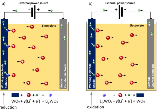
Electrochromism is the unique property of the material whose color changes in response to the insertion/extraction of ions and electrons driven by an external potential. Due to the specific property of tungsten oxide (WOX), developed devices have the ability to change their optical state from dark blue to near or fully transparent in a controllable and reversible way. Such optical switching is performed by insertion/extraction of electrons together with alkali ions such as Li+.
Let’s use the classical electrochemical cell presented in Figure 1.3 to explain the basics of EC device operation. Such electrochemical (or more precisely electrolytic) cell is made of two electrodes immersed in an electrolyte containing ions (i.e. cations). When the external voltage is supplied between electrodes the oxidation and reduction reactions occur respectively on anode and cathode. Two different kinds of EC materials exist, depending if they are colored upon charge insertion (cathodic) or extraction (anodic). As the presented work is focused on devices developed based on cathodic material (WOX), the optically active material (working electrode) is placed on a cathode which attracts cations (Li+). External voltage shuttles ions into and out (reversed polarization) of the material causing coloring (Figure 1.3a) and bleaching action (Figure 1.3b), respectively.
Generalized mechanism of electrochemical reaction for cathodic EC material causing coloring and bleaching action can be expressed by Equations 1.1 and 1.2, respectively.
WOX + y(Li+ + e-) LiyWOX (1.1)
LiyWOX – y(Li+ + e-) WOX (1.2)
10
highly conductive electrolyte is the key to realize EC device with switching time at practical level. From the other hand, high number of electrochemically active centers available for reaction guarantees high contrast between colored and bleach state (high optical modulation).
Figure 1.3. Schematic representation of EC device operation in a configuration of electrolytic cell
during a) coloration and b) bleaching action
1.1.4.Energy efficient concepts
11
electrode, so that the backlight is not required (see Figure 1.4a). The fact that bistable EC display working in reflection mode requires extremely low energy to operate makes it one of the best candidates for these applications.
Figure 1.4. Diagrams showing the principles of energy efficiency concept in a) EC display and b) EC
window; c) estimated values of the heat loss through building elements with possible solutions to reduce the adverse effect of insufficient insulation

![Figure 1.2. EC windows developed via PVD techniques installed by a) VIEW in W San Francisco Hotel, USA [20] and b) SAGE Electrochromics in Library of , While Bear Lake, MN, USA [21]](https://thumb-eu.123doks.com/thumbv2/123dok_br/16693774.743745/43.892.120.778.109.328/figure-windows-developed-techniques-installed-francisco-electrochromics-library.webp)


![Table 2.6. Measured values of the viscosity and the surface tension for each experimental run Run Viscosity [cP] Surface tension [mN m ‐1 ]](https://thumb-eu.123doks.com/thumbv2/123dok_br/16693774.743745/99.892.209.695.268.929/measured-viscosity-surface-tension-experimental-viscosity-surface-tension.webp)