Daniel Alfredo de Sá Pereira
Licenciado em Ciências de Engenharia de Micro e Nanotecnologias
Control of a White Organic Light Emitting Diode’s emission
parameters using a single doped RGB active layer
Dissertação para obtenção do Grau de Mestre em Engenharia de Micro e Nanotecnologias
Orientador: Professor Doutor Luiz Fernando Ribeiro Pereira, Professor Auxiliar,
Departamento de Física, Universidade de Aveiro
Co-orientador: Professora Doutora Isabel Maria das Mercês Ferreira,
Professora Associada, Departamento das Ciências dos Materiais, Faculdade
de Ciências e Tecnologias da Universidade Nova de Lisboa
Júri:
Presidente: Prof. Doutor Rodrigo Martins
Arguente: Prof. Doutor Henrique Gomes
“There is a single light of science,
and to brighten in anywhere is to brighten it everywhere.”
Control of a White Organic Light Emitting Diode’s emission parameters using a single doped RGB layer
Copyright © Daniel Alfredo de Sá Pereira, 2015.
Acknowledgements
Todas as pessoas aqui presentes fizeram, de certa forma, a diferença ao longo destes 5 anos de percurso académico e merecem uma especial menção. Queria agradecer, desde já, a todos os que lá estiveram, nos bons e maus momentos e que, de alguma forma contribuíram para que este momento chegasse.
Gostaria de começar por agradecer ao meu orientador, o Professor Dr. Luiz Pereira, que me recebeu e orientou na Universidade de Aveiro e cujo apoio, dedicação e entusiasmo pela área fizeram toda a diferença ao longo dos vários momentos que constituíram esta fase. Um grande obrigado por tudo. À minha orientadora da FCT-UNL, Prof. Dra. Isabel Ferreira, que me abriu bastantes portas e foi uma grande ajuda nestes últimos anos.
Aos meus pais, Rui e Esmeralda, a quem dedico esta tese, por 23 anos de uma formidável compreensão. Se sou o que sou e se cheguei onde cheguei a vocês o devo e meras palavras não chegam para descrever o meu agradecimento.
À minha irmã Vera que me ensinou que, se fizermos o que gostamos, não temos que trabalhar um único dia nas nossas vidas, ao Ariel, que se conseguir ler isto em português significa que já faz parte da família e ao meu primo Ricardo, que facilmente se tornou um suporte nesta família.
Aos meus tios, António e Irene e aos seus fantásticos filhos Filipa, Bruno e Mariana pelos vários anos de momentos perfeitos.
Ao Engenheiro João Gomes que me recebeu no CeNTI e ao André Pinto pelo apoio na construção dos OLEDs de larga área, um muito obrigado.
A todas as pessoas do Departamento de Física da Universidade de Aveiro que me ajudaram na transição e me receberam como um deles em especial ao Cláudio e à Rosa pela ajuda nas medições de PL e de PLE das minhas amostras.
A special thank you to Dr. Stefan Nowy for the help provided in the Impedance Spectroscopy analysis.
Ao Prof. Dr. Rodrigo Martins e à Prof. Dra. Elvira Fortunato pela criação, promoção e reconhecimento alcançado pelo curso de Engenharia Micro e Nanotecnologias.
À Sónia e à Sara da secretaria do Departamento de Materiais que foram sempre impecáveis quando eu precisei, um muito obrigado.
À Farah, não é preciso dizer nada mas obrigado por todas as conversas, idas aleatórias a Lisboa, interails, passeios e uma amizade como nunca julguei ser possível ter. Estes 5 anos, sem ti, não teriam sido a mesma coisa e apesar de já não sermos praticamente vizinhos, sinto que estamos mais próximos que nunca. O que são uns países entre nós? À Catarina, parceira dos trabalhos, dos projectos, do estudo mas acima de tudo parceira de imensos cafés, idas ao ginásio, chamadas internacionais e uma amizade incondicional. Ao Emanuel, um óptimo grande amigo, ensinaste-me que se dermos um pouco mais de nós, conseguimos chegar lá, acima de tudo em equipa.
Ao João Jacinto, foste a primeira pessoa com quem falei na FCT e 5 anos depois, só tenho a agradecer todo a ajuda, todas as conversas e conselhos e aquele verão fantástico com o pessoal.
pitchos e à Teresa Kullberg que me ensinou que existe muito que se lhe diga na conceção de um pudim de pós. Ao Zé Rui, porque há muito que se lhe diga numa sessão de magia (claro que te tinha que associar a isto).
Ao André Abreu, obrigado por estares sempre do meu lado e pelos jantares, cinemas, idas a Lisboa, gelados,… (ainda me deves a visita a Aveiro). Não me esqueço claro da parceira do GIM, Maggie, e do Samuel e do Hugo.
Aos grandes Júlio Costa (irmão iNOVO), Nuno Coelho (epa quase que transmito sentimentos aqui) e Diogo Vaz (Penus Orniturrincus) pelas noites aleatórias nesse grande Basolho. Às melhores afilhadas do mundo, Joana (diversos cremes nas costas), Sofia (diversos momentos de descontração) e Constança (diversas conversas sobre séries e viagens pela Alemanha), a vocês todos uma palavra chega: ÇIM!
Ao Ricardo, a viagem à Islândia ainda está por realizar e ao Serafim pelos mais variados conselhos nestes últimos anos.
To my fantastic HZB family, Paula, Gianluca, Andrea, Juanita, Omar, Jennifer, Zack, Arturo,
Marina and Guillermo I’ll never forget you and I know that, in the future we will be all together again. You easily became a part of my everyday life so for that I thank you.
À minha recém contratada nutricionista Juliana e aos restantes Aneurécticos, Daniela, Miguel, Zé, Carla, Joana, Alex, Jorge, Silvinha um grande grupo de pessoas.
Ao Diogo Almeida por ter sido uma presença tão importante na minha estadia em Aveiro, seja pela companhia, seja pelas viagens e concertos por esse país fora. To Paulo Laranjeira, because it makes perfect sense to write this in English, for the Tuesdays and Thursdays (and other days) lunch hours. Oh, and for the Kikis.
Abstract
White Color tuning is an attractive feature that Organic Light Emitting Diodes (OLEDs) offer.
Up until now, there hasn’t been any report that mix both color tuning abilities with device stability. In
this work, White OLEDs (W-OLEDs) based on a single RGB blend composed of a blue emitting N,N′ -Di(1-naphthyl)-N,N′-diphenyl-(1,1′-biphenyl)-4,4′-diamine (NPB) doped with a green emitting Coumarin-153 and a red emitting 4-(Dicyanomethylene)-2-methyl-6-(4-dimethylaminostyryl)-4H-pyran (DCM1) dyes were produced. The final device structure was ITO/Blend/Bathocuproine (BCP)/ Tris(8-hydroxyquinolinato)aluminium (Alq3)/Al with an emission area of 0.25 cm2. The effects of the changing in DCM1’s concentration (from 0.5% to 1% wt.) allowed a tuning in the final white color resulting in devices capable of emitting a wide range of tunes – from cool to warm – while also keeping a low device complexity and a high stabilitty. Moreover, an explanation on the optoelectrical behavior of the device is presented. The best electroluminescense (EL) points toward 160 cd/m2 of brightness and 1.1 cd/A of efficiency, both prompted to being enhanced. An Impedance Spectroscopy (IS) analysis allowed to study both the effects of BCP as a Hole Blocking Layer and as an aging probe of the device. Finally, as a proof of concept, the emission was increased 9 and 64 times proving this structure can be effectively applied for general lighting.
Resumo
Um dos maiores fatores de atratividade dos Díodos Orgânicos Emissores de Luz (OLEDs) é a capacidade de tonalizar a cor final a ser emitida. Até aqui, não foram apresentados estudos que misturassem essa capacidade com a estabilidade dos dispositivos. Neste trabalho, foram fabricados OLEDs Brancos (W-OLEDs) baseados numa camada emissora RGB composta por uma blenda de
N,N′-Di(1-naphthyl)-N,N′-diphenyl-(1,1′-biphenyl)-4,4′-diamine (NPB) dopado com um emissor verde, Coumarin-153 e um emissor vermelho, 4-(Dicyanomethylene)-2-methyl-6-(4-dimethylaminostyryl)-4H-pyran (DCM1). A estrutura final de cada dispositivo foi ITO/Blenda/ Bathocuproine (BCP)/Tris(8-hydroxyquinolinato)aluminium (Alq3)/Al para uma emissão de 0.25 cm2. Ao variar a concentração de DCM1 (de 0.5 para 1% wt.), foi possível ajustar a cor branca resultando em dispositivos capazes de emitir uma grande gama de tons – do branco frio ao branco quente – a uma estrutura simples e uma estabilidade alta. Além disso, é feita uma explicação ao mecanismo responsável por este comportamento. Os melhores resultados de electroluminescência (EL) apontam para um brilho de 160 cd/m2 e uma eficiência de 1.1 cd/A, ambos alvos de possíveis melhorias. Um estudo de Espectroscopia de Impedância (IS) foi também realizado para, não só avaliar a capacidade retentora de buracos do BCP, como também uma prova de envelhecimento a que os dispositivos são alvo. Finalmente, como prova de conceito, a emissão foi aumentada em 9 e 64 vezes mostrando, assim a aplicabilidade desta estrutura para iluminação.
Abbreviations
CCT Correlated Color Temperature
CFL Compact Fluorescent Lamp
CIE Commission Internationale de L'éclairage
CRI Color Rendering Index
C153 Coumarin-153
CV Capacitance-Voltage
EBL Electron Blocking Layer
EEW Equal Energy White
EIL Electron Injection Layer
EL Electroluminescence
EML Electroluminescence Layer ETL Electron Transport Layer
HOMO Highest Occupied Molecular Orbital HBL Hole Transport Layer
HIL Hole Injection Layer HTL Hole Transport Layer
ITO Indium Tin Oxide
IS Impedance Spectroscopy
LED Light Emitting Diode
LUMO Lowest Unoccupied Molecular Orbital OLED Organic Light Emitting Diode
PL Photoluminescence
PLE Photoluminescence Excitation PLED Polymer Light Emitting Diode
RGB Red Green Blue
RISC Reverse Intersystem Crossing
R2R Roll-to-Roll
SCLC Space Charge Limited Current SSL Solid State Lighting
TADF Thermally Activated Delayed Fluorescence
Symbols
min minute
VTFL Trap Fill Limit Voltage V
Vt Threshold Voltage V
VΩ Ohmic regime limit voltage V
Vbi Built-in Potential V
Eg Energy Gap eV
E0 Vacuum level eV
Sn Singlet energy level (n=0 –fundamental state, n=1,2,3,… – excited states) Tn Triplet energy level (n=1,2,3,… – excited states)
ℎ Planck constant 6.626*10-34 m2.kg/s
λ Wavelength nm
wt% Weight percentage
𝜀𝑟 Dielectric constant F⋅m−1
Table of Contents
Acknowledgements ... vii
Abstract ... xi
Resumo ... xiii
Abbreviations ... xv
Symbols ... xvii
Table of Contents ... xix
List of Figures ... xxi
List of Tables ... xxv
Objective ... 1
Work structure ... 1
Motivation ... 3
1. Towards OLED lighting ... 3
2. The circadian rhythm ... 3
Chapter I: Introduction ... 5
1. Organic Light Emitting Diode’s operation ... 5
1.1. Hybridization in Organic Semiconductors... 5
1.2. Charge Transport ... 6
1.2.1. The Hopping process ... 6
1.2.2. Space Charge Limited Current ... 7
1.3. Light Generation: Fluorescence and Phosphorescence... 8
2. W-OLEDs for Solid State Lighting ... 9
2.1. Selective doping – the Host:Guest System ... 10
Chapter II: Materials and Structure ... 13
Chapter III: Experimental ... 15
1. Substrate and Sample Preparation ... 15
2. Films Deposition ... 15
3. Device Characterization ... 16
1. Blend Definition ... 17
2. Device Dynamics ... 18
2.1. Electroluminescence Spectra and Figures of Merit ... 18
2.2. Device Stability ... 19
2.3. Photophysical and energy level analysis: operation theory ... 20
3. Optoelectronic Characterization ... 23
4. a.c. analysis ... 26
4.1. Impedance Spectroscopy (IS) ... 26
4.2. Capacitance-Voltage ... 28
4.3. Aging Studies ... 29
5. Large Area ... 30
Chapter V: Conclusion and future trends ... 35
References ... 37
Appendices ... 43
1. Solid State Lighting... 43
2. Color quality of white light sources ... 43
2.1. Figures of merit ... 43
2.2. Light Sources ... 46
3. Radiative and Non-Radiative Transitions ... 47
4. I1 and I2 Optoelectronical Characterization ... 48
5. Impedance spectroscopy of OLED ... 48
5.1. Equivalent circuits ... 49
5.2. Capacitance-Voltage Measurements ... 51
List of Figures
Figure 1 – Schematic of a multi-layer Organic Light Emitting Diode (OLED) and device operation. Holes are injected through the anode while electrons are injected through the cathode. Each layer was left unnamed intentionally (adapted from [8]) ... 5 Figure 2 – a) Bonding in a carbon-based molecule with sp2 hybridization. b) Benzene molecule and its delocalized states forming the LUMO and HOMO levels (adapted from [11]). ... 6
Figure 3 – Hopping process in an organic molecule as a result of the orbitals overlapping (dashed lines) allowing the carrier to hop between them when an electric field is applied. ... 7
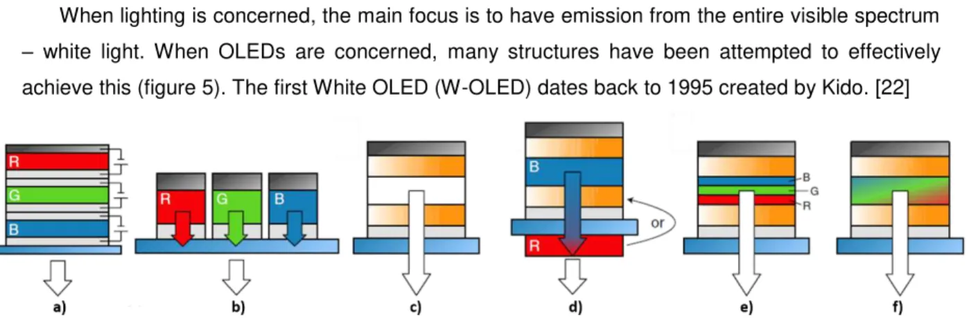
Figure 4 – IV dependence with the applied voltage in an organic semiconductor considering a trap-free and a trap-dependent (either shallow or deep) model. The effects of the trapped carrier in the mobility is not described. The dynamics of the junction created between a metal and an organic semiconductor can be found in [17]. ... 8 Figure 5 - State of the art on applied structures used for white light emission on bottom emitting W-OLEDs. a) vertically stacked b) pixelated monochrome, c) single-emitter-based, d) blue OLEDs with downconversion layers, e) single OLEDs with a sublayer EML design and f) single emitting layer OLEDs based on a selective doping process. ... 9
Figure 6 – Final device structure composed with three organic layers sandwiched between two electrodes. Adding more would allow for a more efficient device at the expense of its simplicity. The HTL is used also as EML being based on the Host:Guest system. Holes are injected into the HTL while electrons in the ETL. Finally, because electrons have lower mobility, a HBL is introduced to assure the recombination in the HTL (Chapter I section 2.1.). ... 13 Figure 7 – Chemical structure of all organic small molecules used for the OLED deposition. The final device structure is ITO/NPB:x%DCM1:y%C-153/BCP/Alq3/Al as anode/HTL (and EML)/HBL/ETL/cathode respectively. x% and y% stands for small %wt of the dopants. All chemical structures were purchased from Sigma Aldrich. ... 14
Figure 8 – Schematics showing all process to obtain a small area bottom-emitting OLED from a glass substrate containing a thin ITO film (a) leading to its patterning (b), cleaning process (c) and thermal evaporation of the blend EML (d), the HBL (e), the ETL (f) and the cathode (g) respectively. 4 different emissive areas of 25 mm2 (h) were produced. ... 15 Figure 9 – Normalized Electroluminescence spectra of devices I1, I2 and I3 at 32 V. The color tuning, is achieved by the increase of the peak intensity at around 550 nm changing the overall emitted color. The significantly high voltage is the result of a high resistivity ITO film. ... 18
Figure 11 - a), b), c) EL spectra for the tunable W-OLED i.e. for the devices composed with different concentration of DCM1 I1, I2 and I3 respectively. The inset on each graph shows a picture of the different device at 32 V for a naked eye interpretation. The applied voltages were 26, 28, 30 and 32 V for all samples. ... 20 Figure 12 – Normalized PL spectra of NPB, C153 and DCM1 independently. ... 21 Figure 13 – EL spectra for a device with an active layer of NPB:1%C153 showing a slight blue-shift
of C153’s main emission. ... 22 Figure 14 – Energy levels of all layers constituent of the devices (table 1). ... 22 Figure 15 – Active layer operation. When electrons are injected, they channel to DCM1 in a non-radiative way without C153 (a) or when C153 is added (b) resulting in the emission of light through DCM1. When its concentration is decreased, the emission of C153 (c) is promoted resulted in the increase of the correspondent peak. ... 23 Figure 16 – JVL curves for devices I1, I2 and I3. The Luminance was taken without background light to reduce ambient effects. ... 24
Figure 17 – a) log(IV) curves for the device I3 displaying the ohmic and SCLC regions. The curve’s slope is an evidence of a deep trap behavior (m>2). b) Efficiency dependence with voltage of device I3 for an OLED with emission area of 25 mm2. ... 25 Figure 18 - a) Capacitance and dielectric loss curves for the device at 0 V dc typical for the ohmic regime. b) Cole-Cole plot, i.e. the dielectric loss as a function of the capacitance for the same device. Following a model described in the inset with a parallel RC for R1=110 Ω and C1=8.75 nF, a simulated
curve was drawn showing a good fitting can be obtained for this model. ... 26 Figure 19 – a) Capacitance and dielectric loss curves for the device at 20 V dc to assure the SCLC showing interfacial changes in the capacitance dielectric loss values b) Cole-Cole plot, i.e. the dielectric loss as a function of the capacitance for the same device. Following a model described in
the inset with a two sets of parallel RC in series for R1=17500 Ω, R2=105 Ω, C1=9 nF and C2=0.02
nF a simulated curve was drawn showing a good fitting can be obtained for this model. The equipment interference at low frequency results in a deviation of the obtained values. ... 27 Figure 20 – Capacitance-voltage measurements of the device shown in figures 9 and 10 at a fixed frequency of 1000 Hz. ... 28
Figure 21 – a) Capacitance and dielectric loss for the same device at 0 V dc after 0, 24, 48 and 72h at room temperature and ambient air. b) Correspondent Cole-Cole plots overlapped with its simulated curves using the R1 and C1 values of table 6 always assuming a parallel RC model. ... 29
the EL spectra for a typical barrier limit white emission. This barrier white emission was obtained for concentrations of 98.3%:1%:1 of NPB:C153:DCM1 respectively. ... 31 Figure 24 – a) cool white OLED with an active layer of 16cm2 and highlighted defects. b) JV curve for the device in figure 24a with threshold voltage of around 11 V. Inset shows the EL spectra for a cool white emission with a low emission from DCM1 which may be the result of a low material evaporation. Increasing this should increase the amount of DCM1 in the final evaporated blend. This cool white emission was obtained for concentrations of 98.3%:1%:0.7 of NPB:C153:DCM1 respectively. ... 32 Figure 25 – a) cool white OLED with an active layer of 16cm2 produced with an optimized ITO patterning. b) JVL characteristic for this device showing a voltage drop for the threshold voltage as a
result of a decrease in the ITO’s resistivity. ... 33 Figure 26 – CIE 1931 (x,y) including different color regions, planckian locus and color temperatures [2] ... 44
Figure 27 – The effects of light sources with high (90) and low (60) Color Rendering Indexes. A high CRI means that a color source effectively covers the entire visible spectrum being able to reproduce all the surrounding colors. Low CRI, on the other hand, may lack Red, Green or Blue counterparts resulting in inefficient reproducibility of the surrounding environment. (adapted from [63]) ... 45
Figure 28 – CCT values for different sources including range for the produced OLEDs. ... 45 Figure 29 – Energy transitions in a Host:Guest system (section 2.1.) namely the energy transfer (either through radiative a) and non-radiative i.e. the Förster transition b)) and the carrier trapping c). ... 47
Figure 30 – a) JV curves and b) current efficiency values for devices I1 and I2. ... 48 Figure 31 – IV curve of an ideal diode. For IS measurements, a bias voltage VDC is chosen followed by the appliance of an alternating signal VAC(t) and the corresponding IAC(t) is obtained. [60] ... 48
Figure 32 – Models considered for an IS analysis based on a) single and b) double parallel RC circuits ... 50
Figure 33 – CV measurement of an OLED device. The values were left out purposely being of particular interest the behavior and not the constitution of the device (adapted from [60]) ... 51
List of Tables
Table 1 – Parameters considered upon the deposition of each material. Because the dyes’
concentration was small compared to the Host’s, its density values were not taken into consideration.
... 14 Table 2 – blend combinations studied for the production of the color tunable white OLEDs. ... 17
Table 3 – Blend concentration for each sample produced. In order to decrease the number of degrees of freedom, one of the concentrations was kept constant, in this case the Coumarin-153. The experiments conducted that showed that the white color in our devices is more susceptible to changes with DCM1. ... 17 Table 4 – Figures of merit for devices I1, I2 and I3 at 32 V calculated from the relative intensity of all three devices (figure 9). ... 18 Table 5 – Color coordinates for devices I1, I2 and I3 at voltages between 26 and 32 V corresponding to the EL spectra shown in figure 3. ... 20
Table 6 – Simulated C1 and R1 with calculated relaxation frequency for the device characterized on figure 21 after 0, 24, 48 and 72h. ... 30
Table 7 – Simulated C1, R1, C2 and R2 with calculated relaxation frequency, fr1 and fr2, for the device characterized on figure 19 after 0, 24, 48 and 72h. ... 30
Objective
Organic Light Emitting Diodes (OLEDs) promise to shape the entire reality of general lighting technologies. This thesis aims to produce Color tunable White OLEDs (W-OLEDs) based on a single doped RGB active layer. The color tunes are obtained by changing one of the dopant’s concentration,
being the different tunes analyzed. Once the proper tunes are obtained, the scale up of the devices to large area was attempted.
Work structure
Motivation
1. Towards OLED lighting
The energy demand nowadays has brought an exhausting use of the natural resources. Considering that 19% of all the electricity consumed is for artificial lighting which corresponds to an emission of 1900 Mt of CO2 every year [1], improvements towards a more eco-friendly future is urgent. Looking for the “ideal” lighting system, the research for a power efficient, disposable, non-harmful and long-lasting technology is thought. And throughout history, many attempts have been made to effectively reach this ideal technology, each of them lacking one or more of the goals referred as it will be explained further ahead.
The scientific community has been looking for more efficient ways to produce light. Appendix 1 shows how this technology has been evolving resulting in the commercially available Light Emitting Diodes (LEDs) which are more economical and have longer lifetimes than the past bulb and fluorescent lamps. However, LEDs have several limitations since most of them use rare materials such as Ga, As, In, etc. and soon enough problems of scarcity can be faced. [2]
Organic Light Emitting Diodes (OLEDs) come to help solving this problem since they use organic materials instead of inorganic and can be produced in a large set of substrates (which includes large area panels). [3] Therefore, it can shake the current lighting paradigm as a not so futuristic technology (not anymore at least) since it allows for a materials’ internal efficiency of, theoretically 100%, can be fabricated in rigid or flexible substrates, uses organic disposable materials with zero harm to the environment and allow for the possibility of obtaining high brightness devices. All of this not mentioning its market attractiveness. Putting together all these qualities, OLEDs have a huge market
interest in the near future for the everyday life’s artificial lighting. The market of OLEDs is already ON and soon can replace the current LED technology.
2. The circadian rhythm
It is interesting to analyze the color tuning ability that OLED devices may achieve. Theoretically, by simply changing the materials (or their proportion) or the overall device structure, it is possible to obtain sources capable of emitting different shades of white specific environments and applications. But, forgetting the obvious academic and artistic interest what is the main market interest here? Why should we care if we are surrounded by a cool white (with blueish tone) or a warm white source (with a greenish/reddish tone)?
Life on Earth is controlled by the 24h hours of the solar cycle that synchronizes the biological circadian cycle (or rhythm) with physiology and behavior patterns with light serving as a resettle of this rhythm. And we are surrounded by light, either environmental or artificial. This last one aims to reproduce the surrounding colors in the absence of environmental light. The problem is that these
After studies in animals had suggested a role for a non-rod, non-cone photoreceptor in circadian responses to light, melanopsin was identified as the photopigment present in those specialized photoreceptors. In this matter, critical to our sleep/wake cycle is melatonin, segregated by the hypothalamus, a hormone that promotes sleep, and can be stimulated by the kind of light we are surrounded to due to special non-visual photoreceptors at the retina stimulated with the blue color. It is also being used as a sleep aid and in the treatment of some sleep disorders. [4] So depending on the surrounding light, this hormone can be segregated or inhibited. Morning light, for example, is light that is received during the first hours of the day and is very effective at resetting the rhythm. Getting strong blue rich light early in the morning every day helps to stay in tune with the timing of daily obligations since bluish white light stops melatonin production. Evening light, on the other hand, as long as it is dim and low in blue (short wavelength) content, can help relaxing and prepare for sleep (yellowish white light allows for melatonin production). [5] Bright evening light, though, suppresses melatonin production and delays sleep. And this is where the target application comes in place.
Chapter I: Introduction
1. Organic Light Emitting Diode’s operation
Tang and VanSlyke (1987) and Burroughes et. al. (1990) were the first to report low voltage electroluminescence from thin organic films made of small-molecular-weight molecules and polymers, respectively. Ever since, the possibility of applying organic materials on lighting systems has emerged and research on this topic has brought a big increase on the number of reports regarding this subject. The possibility of light emission from organic materials has, therefore emerged a wider range of possibilities, being the first step towards the recent developments of Organic LEDs (OLEDs) and Polymer LEDs (PLEDs).[6],[7]
An OLED is a lighting device capable of emitting white light through the use of organic molecules. Generally, these devices are composed of different organic layers sandwiched between two electrodes. A diagram describing the main operation of OLEDs can be found in figure 1. Each layer has a different purpose in the overall working of the device, so each organic material (either small molecule or polymer) must be chosen according to their function in the final structure. The main mechanism, is similar to the Light Emitting Diode’s (LED) behavior. [8]
Figure 1 – Schematic of a multi-layer Organic Light Emitting Diode (OLED) and device operation. Holes are injected through the anode while electrons are injected through the cathode. Each layer was left unnamed intentionally (adapted from [8])
Upon application of an external bias, electrons and holes are injected by the electrodes into the p and n organic layers, travelling across their molecular structure until they recombine in the emissive area. Here, excitons (coupled state between electrons and holes) are formed through Coulomb interaction between the injected carriers in a process called charge recombination. The rapid decay of the electron to a lower energy state, allows for the emission of light with a wavelength corresponding to the energy transition of the carrier where the emission takes place. [9], [10]
1.1. Hybridization in Organic Semiconductors
the nature of the sp2 bonds gives rise to carrier conduction forming, for example, the benzene ring that will serve as an example further ahead. In this type of hybridization (figure 2a), there are three hybrid sp2 orbitals and one 2pz that allows for the formation of three high energy σ bonds (one per each hybrid orbital) and two low energy π (one bonding, denoted π and one antibonding, denoted
π*). When the benzene ring is considered (figure 2b), with a configuration –C=C–C=C–C=C–, the double bonds are composed by one σ and one π and because this last one is of low energy, the electrons can, under an electrical field, move throughout the molecule in delocalized states (not associated with an atom but within an orbital of several adjacent atoms).
Figure 2 – a) Bonding in a carbon-based molecule with sp2 hybridization. b) Benzene molecule and its
delocalized states forming the LUMO and HOMO levels (adapted from [11]).
Increasing the number of carbon atoms in the molecule, an energy cloud composed with these delocalized electrons and their ability to roam freely in the molecular orbital is formed. These occupied states, more specifically the highest energy counterpart, forms the so called Highest Occupied Molecular Orbital (HOMO). The antibonding unoccupied states π*, or its lowest energy counterpart forms the Lowest Unoccupied Molecular Orbital (LUMO). Between the HOMO and the LUMO of each material is the so called energy gap, Eg prohibited for the delocalized electrons.[11],[12]
These energy levels are a characteristic of the organic semiconductor the same way the valence and the conduction band are a characteristic of an inorganic one. By using different layers composed of different materials, a structure capable of guiding carriers through the organic layers is built by either enhancing their injection or promoting their blockage always having in mind the differences in charge mobility (chapter I section 1.2.1.). It is then possible to denote different layers according to 1) the charge it relates to (hole or electron) and 2 its basic function (injection, transport or blockage) giving rise to the Hole and Electron Injection (HIL and EIL respectively), Transport (HTL and ETL respectively) and Blocking (HBL and EBL respectively) layers. Finally, the layer where recombination and emission takes place is called Electroluminescence Layer (EML).
1.2. Charge Transport
1.2.1. The Hopping process
Once available for conduction, electrons and holes travel freely across the inorganic
semiconductor’s matrix in the conduction and valence bands, respectively. Carrier transport in organic
semiconductor based devices, on the other hand, is different from this behavior. It is based on a hopping process (figure 3) - interference between the delocalized orbitals π and π* with the applied electric field. As seen before, the main consideration is the typical structure of the benzene ring where
the electron cloud results from the overlapping of the orbitals. An electron in one of these LUMO orbitals, although still connected to its original carbon atom, is susceptible to hop into a neighbor orbital if an electric field is applied, vacating it and allowing for another electron to hop into it. This carrier transport gives rise to the electrical conduction. A similar behavior can be seen in the HOMO orbitals for the hole conduction. This process will have a big effect on the carrier mobility. Although delocalized, the carrier never loses the identity to its atom counterpart, so the mobility will be several orders of magnitude lower than a carrier travelling in an inorganic semiconductor. Also, the bonding delocalized orbital has a more consistent structure than the non-bonding resulting in a higher mobility
for HOMO’s holes in the when compared to the LUMO’S electrons.[13]
Figure 3 – Hopping process in an organic molecule as a result of the orbitals overlapping (dashed lines) allowing the carrier to hop between them when an electric field is applied.
1.2.2. Space Charge Limited Current
When carriers are injected into their layers, i.e. when a voltage is applied, the unorganized structure of the organic semiconductors compared to the organized for the inorganic, implies a completely different behavior for carrier conduction. The models describing the timeframe after the carriers are injected into the organic layers are shown in figure 4.
At low applied voltages, even using electrodes with considerably different energy barrier in the metal semiconductor junction, both anode and cathode are able to equally inject the same amount of carriers being the current only dependent on the resistance of the material – Ohmic region where
𝐼 ∝ 𝑉. Increasing the applied voltage until a certain value (Ohmic regime limit voltage, VΩ) leads to a
difference in the injection performance of the electrodes if, in a finite time, one of them is considerably different from the other, meaning that one electrode is effectively injecting a carrier while the other is ineffectively pushing it which leads to an increase of current inside the device – Space Charge Limited Current (SCLC) region where 𝐼 ∝ 𝑉𝑛 and 𝑛>1.
In the SCLC, the unorganized structure allows the appearance of traps that may fall within the energy gap of the semiconductor. To analyze the effects of these traps, considering first a trap-free model and comparing it with two trap-dependent models, each one categorized by their proximity to the Fermi level: shallow trap if it is energetically close or deep trap if far. In the trap-free model, n=2 as a result of no trapping of carriers, meaning that the current flows accordingly to the mobility of these carriers and the physical and electrical properties of the layer. In the shallow-trap model, the
Electron
trapped carriers do not contribute to the current, leading to its decrease, but still dependent on V2. Increasing the applied voltage, all traps will eventually be filled. Near this limit voltage value (Trap Fill Limited Voltage VTFL), there’s a slight increase in the current (Vn with n>2) followed by the same behavior described before. Finally, for the deep-trap model, a discrete distribution of traps is considered and different models must be applied to better describe the transport mechanisms. By considering either a Gaussian or an Exponential distribution, the behavior is similar only characterized by different expressions, for VΩ<V<VTFL, the current is dependent of 𝐼 ∝ 𝑉𝑛 and 𝑛>2. Above VTFL the exhibited behavior is the same as described before.[14], [15], [16]
Figure 4 –IV dependence with the applied voltage in an organic semiconductor considering a trap-free and a trap-dependent (either shallow or deep) model. The effects of the trapped carrier in the mobility is not described. The dynamics of the junction created between a metal and an organic semiconductor can be found in [17].
1.3. Light Generation: Fluorescence and Phosphorescence
Light is emitted whenever there’s radiative decay (emission of a photon) of an electron from an excited energy level to the fundamental state, being the wavelength of the photon emitted equivalent to the energy decay of that electron. In organic semiconductors, this radiative decay is a result of the recombination between carriers to form an exciton.
Understanding the difference between fluorescence and phosphorescence implies knowledge of electron spin and the differences between singlet and triplet states. When an excitation occurs from the fundamental state and depending on the spin of the level it achieves, there are two types of excited levels. In terms of terminology, a singlet (triplet) state occurs when the spin of an electron in
the π* orbital and that of the remaining electron in the π-orbital are antiparallel (parallel) and so add up to a total spin of zero (one). Therefore, because a singlet exciton has a spin multiplicity of 0 (MS=0) and the triplet exciton 1 (MS = -1, 0 and 1), on average 75% of the excitons formed are triplet states, with the remaining 25% being singlets. In the fundamental state, electrons have non-paired spins, typical of a singlet level. The triplet state has a smaller energy than its singlet counterpart because of the repulsive origin of its electron spins.
transition involves a triplet-to-singlet state (T1→ S0) it is called phosphorescence, though this implies the use of intermediate materials (such as rare earth or transition metals) for radiative transition that reduce the permanence time (increasing the transition probability) of an electron in the excited triplet state. Otherwise, the energy loss would be made by thermally (i.e. non-radiatively). Phosphorescent devices have a theoretical efficiency up to 100% as it considers both singlet-to-singlet and triplet-to-singlet transitions.[3],[18],[19] This results in devices with considerably higher external efficiency. [20]
Recently, there have been reports on Thermally Activated Delayed Fluorescence (TADF) to achieve 100% efficiency on fluorescent materials via Reverse Intersystem Crossing (RISC) which is based on the use of temperature to allow for the transition of an electron from an excited triplet to an excited singlet. [21]
2. W-OLEDs for Solid State Lighting
When lighting is concerned, the main focus is to have emission from the entire visible spectrum
– white light. When OLEDs are concerned, many structures have been attempted to effectively achieve this (figure 5). The first White OLED (W-OLED) dates back to 1995 created by Kido. [22]
Figure 5 - State of the art on applied structures used for white light emission on bottom emitting W-OLEDs. a) vertically stacked b) pixelated monochrome, c) single-emitter-based, d) blue OLEDs with downconversion layers, e) single OLEDs with a sublayer EML design and f) single emitting layer OLEDs based on a selective doping process.
Figure 5 a) and b) shows the emission of white light as a sum of independent Red, Green and Blue emitters either with individual electrodes or as a pixelated structure, commonly used on the current OLEDs flat panel displays. These two structures involve comparably complicated structuring processes which would increase the final production costs’. [23], [24] So, in order to decrease these, a single emitting layer must be considered. A single molecule, for example, may be synthesized to emit over the entire visible spectrum (figure 5c) although it is not easy to tune the color without affecting device performance. Also, these molecules are usually related to poor device efficiencies [20] [25] The use of an external (or internal) downconversion layer (figure 5d) is based on high energy emissions. Part of this light excites another molecule resulting in its main emission, the sum being white light. This implies a slightly more complicated structure (one or two downconversion layers) than the single emitting layer, while resulting also in poor color rendering because of poor overlapping
here is that there must be a trade-off between the device complexity and efficiency when lighting is concerned. So far, there has not been a report of a blended RGB capable of efficiently emitting with a great level of stability. [28] To assure the highest quality for the lowest complexity, either the emissive layer or the whole device must be tailored. The purity of a white source can be characterized by the corresponding figures of merit, described more extensively on appendix 2: the Commission Internationale de L'éclairage (CIE), the Correlated Color Temperature (CCT) and the Color-Rendering Index (CRI). Also, devices with high color stability with the applied voltage/current prevent shifts in terms of CIE that will be perceived by the human eye. [29]
2.1. Selective doping – the Host:Guest System
The Host:Guest System is the most used technique to obtain white light since it allows for the production of simple devices with high efficiency. [30] This system consists of a single EML comprising one host matrix – donor – and one or more dopants – acceptor dyes – mixed inside the matrix allowing for light emission in these materials. It involves two predominant mechanisms: the
energy transfer and the carrier trapping. Considering the energies’ corresponding vibrational levels
of the fundamental state S0 and excited state S1 of both donor and acceptor molecules, one can easily draw the schematics of these main mechanisms (appendix 3).
The energy transfer, more specifically, can be a result of radiative and non-radiative transitions. In the radiative transition, after an excitation of a donor electron to its excited level and subsequent energy loss by non-radiative transitions – phonons – to the lowest excited level, a photon with lower energy is emitted. This photon will then be absorbed by the acceptor resulting in the transition of one of its electrons from the fundamental state to the excited level of the guest. After energy relaxation, photons with wavelengths of the corresponding final radiative transitions are emitted (appendix 3, figure 29a). This process will only happen if there is an overlap between the emission of the dopant and the absorption of the acceptor. The non-radiative transition involves a dipole-dipole interaction with long-range separation (~30-100 Å) between an excited electron of the donor and an electron in the fundamental state of the acceptor (and their corresponding holes) allowing it to transfer energy electrostatically, also known as the Förster transition (appendix 3, figure 29b).[31] [32] This energy transfer can be explained as
D*+A → X→D+A+ℎ𝑣,
where D*, A, X, D and ℎ𝑣 stand for excited donor, ground state acceptor, intermediate excited state (ground state donor and excited acceptor), ground state donor and acceptor and energy of the emitted photon, respectively. [33] A short range interaction known as the Dexter transition, is not considered because the host and guest molecules will fall far from the Dexter range. [31]
In the carrier trapping, the guest’s HOMO and/or LUMO levels must fall within those of the hosts’
Chapter II: Materials and Structure
The device’s physical characteristics must be tailored to optimize the structure and stabilize white light emission while also meeting the requirements of a Solid State Device – simple and efficient. This
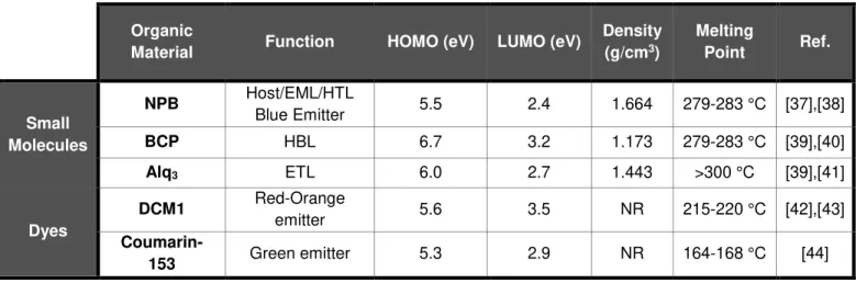
project’s device (figure 6) has three organic layers between the electrodes. The final device structure is: Anode/HTL/HBL/ETL/Cathode with the HTL serving also as EML based on the Host:Guest system (Chapter I, section 2.1.). Finally, because all of the organic materials used are small molecules, a thermal evaporation technique is used.[36] Figure 7 shows the chemical structure of the final organic molecules used to build each device while table 1 describes the basic parameters important for device production and characterization.
Figure 6 – Final device structure composed with three organic layers sandwiched between two electrodes. Adding more would allow for a more efficient device at the expense of its simplicity. The HTL is used also as EML being based on the Host:Guest system. Holes are injected into the HTL while electrons in the ETL. Finally, because electrons have lower mobility, a HBL is introduced to assure the recombination in the HTL (Chapter I section 2.1.).
Figure 7 – Chemical structure of all organic small molecules used for the OLED deposition. The final device
structure is ITO/NPB:x%DCM1:y%C-153/BCP/Alq3/Al as anode/HTL (and EML)/HBL/ETL/cathode respectively.
x% and y% stands for small %wt of the dopants. All chemical structures were purchased from Sigma Aldrich.
Table 1 – Parameters considered upon the deposition of each material. Because the dyes’ concentration was small compared to the Host’s, its density values were not taken into consideration.
Organic
Material Function HOMO (eV) LUMO (eV)
Density (g/cm3)
Melting
Point Ref.
Small Molecules
NPB Host/EML/HTL Blue Emitter 5.5 2.4 1.664 279-283 °C [37],[38]
BCP HBL 6.7 3.2 1.173 279-283 °C [39],[40]
Alq3 ETL 6.0 2.7 1.443 >300 °C [39],[41]
Dyes
DCM1 Red-Orange emitter 5.6 3.5 NR 215-220 °C [42],[43]
Coumarin-153 Green emitter 5.3 2.9 NR 164-168 °C [44]
Coumarin-153 (Green Guest)
Chapter III: Experimental
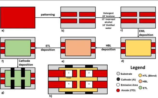
Figure 8 – Schematics showing all process to obtain a small area bottom-emitting OLED from a glass substrate
containing a thin ITO film (a) leading to its patterning (b), cleaning process (c) and thermal evaporation of the blend EML (d), the HBL (e), the ETL (f) and the cathode (g) respectively. 4 different emissive areas of 25 mm2
(h) were produced.
The production (figure 8) and characterization of OLEDs follows a strict procedure which includes three main phases.
1. Substrate and Sample Preparation
In glass substrates with a thin ITO film deposited (a) (30-60 Ω/sq from Delta Technologies), adhesive tape was used to cover the desired patterns for the electrodes (either small or large area). With a mixture of Zinc Powder and Hydrochloric Acid, the uncovered ITO was removed, (b) followed by washing in water and removal of the tape. The substrates were then cleaned in detergent, then washed in Acetone for 20 min, Isopropyl alcohol for 15 min and distilled water for 10 min (c). The samples used as EML were weighed and then mixed under magnetic stirring for no less than 2 hours.
2. Films Deposition
Most of the work was conducted in the Physics department at the University of Aveiro and the large area devices were produced in CeNTI – Centre for Nanotechnology and Smart Materials.
turbomolecular pump was used. The large scale devices were produced using a Kurt J. Lesker Spectros 150 automated system, containing 5 crucibles and a cryogenic pump for high vacuum to a closer-to-industry production.
With a pressure of no higher than 10-5Pa the evaporation process starts. To control each layer’s final thickness, a high sensitivity piezoelectric sensor is used and, by changing the applied power, the evaporation rate is controlled to a maximum value of 4 Å/s to allow for uniform films. All blend (d) tests (50 Å thick) were followed by the deposition of 100 and 300 Å of BCP (e) and Alq3 (f) respectively. Finally, aluminum (g) was deposited with a thickness of 1500+/-200 Å. To prevent aluminum oxidation and/or diffusion into the organic layers, the chamber was stored in vacuum for 15 minutes to cool down after deposition.
3. Device Characterization
All the current density–voltage (JV), luminance–voltage (LV), electro-luminescence (EL), Impedance Spectroscopy (IS) and Capacitance-Voltage (CV) measurements were performed in air in non-encapsulated devices at room temperature right after each evaporation process. For the EL spectra measurement, an Ocean Optics USB4000 spectrometer was used. The JVL characteristics were measured with a Keithley source meter 2425 model and Minolta Colormeter LS-100. From the JVL data, the current efficiency (cd/A) was calculated, a typical parameter in the light emitting devices. In parallel, the dynamic range of the light emission (the applied voltage region where the emission is quite linear) was obtained from the photometric efficiency obtained with the LV graph. IS and CV measurements were performed with a Fluke PM6303 RLC Meter. The photophysical properties –
Chapter IV: Results and Discussion
1. Blend Definition
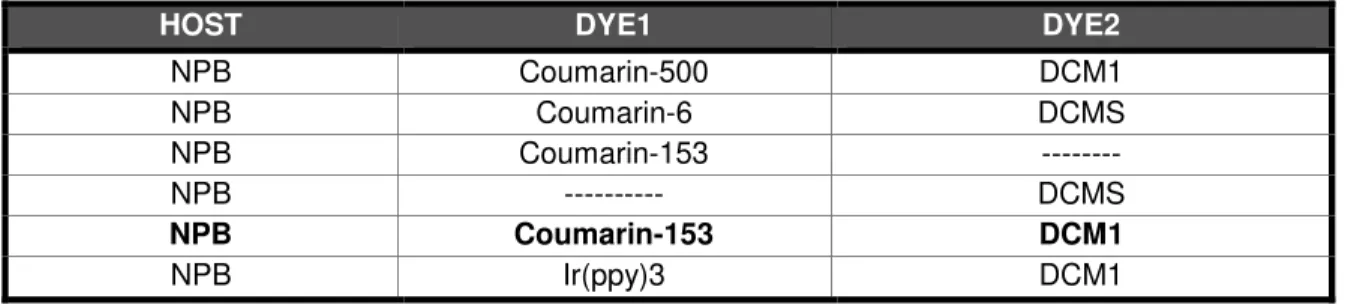
As previously discussed, the main objective was to produce color tunable W-OLEDs based on a single emitting RGB blend that, by changing the concentration of one of its components, would allow for a set of devices capable of emitting different types of white light (from cool to warm). To obtain a low complexity structure, the Host:Guest system with a blue emitting host doped with a green and a red guest dyes, was considered. Also, besides the color tuning ability, the devices should be flexible in terms of the applied potential, i.e. its color properties should remain the same for the human eye when different voltages were applied. To effectively achieve these properties, many blends were studied, and all their Current Density-Voltage-Luminance (JVL) and Electroluminescence (EL) characteristics studied in order to effectively choose the best blend possible for the desired characteristics. Table 2 shows the main blends studied using different Coumarin-related and DCM-related green and red wavelengths, respectively always having NPB as blue emitting host. Ir(ppy)3 was also considered for green dye but, because this is a phosphorescent material (see section 1.3.) and the results weren’t improved, it was later replaced. The best combination (bold) have its materials shown in figure 7 and the concentrations used in table 3.
Table 2 –blend combinations studied for the production of the color tunable white OLEDs.
Table 3 – Blend concentration for each sample produced. In order to decrease the number of degrees of freedom, one of the concentrations was kept constant, in this case the Coumarin-153. The experiments conducted that showed that the white color in our devices is more susceptible to changes with DCM1.
Comparing this structure to other reports, this one is much simpler (only three organic layers) which goes accordingly to the application in mind. [45] Next sections show the main characterization for each sample considered on table 3. Each device was built at least twice to verify the reproducibility of the final structure. The best result of each test is, therefore shown though they didn’t present significant differences.
HOST DYE1 DYE2
NPB Coumarin-500 DCM1
NPB Coumarin-6 DCMS
NPB Coumarin-153 ---
NPB --- DCMS
NPB Coumarin-153 DCM1
NPB Ir(ppy)3 DCM1
SAMPLE HOST DYE1 (x) DYE2 Terminology
I1 NPB DCM1 (0.5% wt.) Coumarin-153 (1% wt.) Cool White
I2 NPB DCM1 (0.7% wt.) Coumarin-153 (1% wt.) Barrier Limit White
2. Device Dynamics
2.1. Electroluminescence Spectra and Figures of Merit
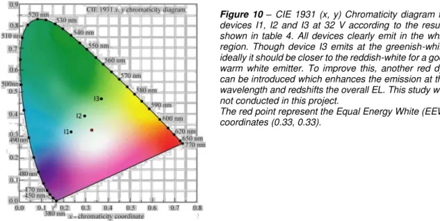
Figure 9 shows the EL spectra of devices I1, I2 and I3 overlapped with the visible spectrum. The main emission covers almost the entire visible region with a lower evidence between the 625 and 700 nm. By increasing DCM1’s concentration, the middle peak at around 475 nm decreases indicating an interaction between different materials. Also, the third peak slightly redshifts from around 535 to 550 nm and its relative intensity increases which indicates that this belongs to the emission of DCM1. With these interactions, the color tuning is achieved with DCM1 concentrations ranging from 0.5% (cool white) to 1% (warm white) with its barrier limit white at around 0.7%. This effect is therefore translated in terms of the correspondent figures of merit (appendix 2) shown in table 4 where the color coordinates (figure 10) change but always stay within the white region. The devices also show high values of CRI meaning a high capability of reproducing the colors of an object when illuminated with these sources, similar to other light sources (appendix 2.2.) proving the applicability of this device to general lighting. The CCT range goes even further than the typical known range for LEDs, 3000 to 7000 K (appendix 2.1.), allowing for a wider range of color tunes.
Table 4– Figures of merit for devices I1, I2 and I3 at 32 V calculated from the relative intensity of all three devices (figure 9).
SAMPLE CIEx CIEy CRI CCT (K)
I1 0,238 0,317 91 2 10500
I2 0,296 0,389 90 2 5100
I3 0,375 0,484 89 2 3200
The evaporation process didn’t offer a temperature controlled evaporation but, as the results were
reproducible, it is safe to assume that the concentrations were correct. Still, this is just a supposition as a more detailed study must be conducted.
2.2. Device Stability
To assess on the stability of a lighting source, different voltages were applied across the device and the overall emission studied. Figure 9 already showed the main emission of the set of devices at 32 V but nothing can be extrapolated only with these particular values. So, a stability test, with voltages between 26 and 32 V, was conducted as seen in figure 11.
Figure 10 – CIE 1931 (x, y) Chromaticity diagram for devices I1, I2 and I3 at 32 V according to the results shown in table 4. All devices clearly emit in the white region. Though device I3 emits at the greenish-white, ideally it should be closer to the reddish-white for a good warm white emitter. To improve this, another red dye can be introduced which enhances the emission at this wavelength and redshifts the overall EL. This study was not conducted in this project.
The red point represent the Equal Energy White (EEW) coordinates (0.33, 0.33).
Figure 11 - a), b), c) EL spectra for the tunable W-OLED i.e. for the devices composed with different concentration of DCM1 I1, I2 and I3 respectively. The inset on each graph shows a picture of the different device at 32 V for a naked eye interpretation. The applied voltages were 26, 28, 30 and 32 V for all samples.
Table 5 shows the translated effects of the devices in terms of color coordinates. These values have a significantly high level of stability, given the low shift in color coordinates when different voltages are applied. The biggest shift is 0.010 which is undetectable by the human eye in the same color region. These results come after supposedly all traps (both natural NPB traps – Chapter I, section 1.2.2. – and energy levels of the dyes) quickly being filled, not contributing to big changes in the color coordinates hence increasing the stability. The quick saturation of traps can be attributed to the use of low level of dyes’ concentration.
Table 5 – Color coordinates for devices I1, I2 and I3 at voltages between 26 and 32 V corresponding to the EL spectra shown in figure 3.
2.3. Photophysical and energy level analysis: operation theory
Taken into account the results in terms of color tuning and stability, the dynamics inside the blend must be understood in order to effectively allow for an improvement of the whole blend. In fact, the choice of DCM1 arose because this is a typical red emitting dye, used for enhanced luminance in red emitting devices [46] with emissions above 600 nm while C153 was chosen because it is a green
Sample Voltage (V) CIEx diff CIEy diff
I1
26 0.225 --- 0.325 ---
28 0.231 +0.006 0.315 -0.010
30 0.238 +0.007 0.314 -0.001
32 0.238 0 0.317 +0.003
I2
26 0.295 --- 0.422 ---
28 0.291 -0.004 0.399 -0.003
30 0.296 +0.005 0.393 -0.006
32 0.297 +0.001 0.389 -0.004
I3
26 0.372 --- 0.501 ---
28 0.377 +0.005 0.498 -0.004
30 0.372 -0.005 0.490 -0.002
32 0.375 +0.003 0.484 -0.006
emitting dye [47] with its main emission around 500 nm, according to the supplier. Upon studying the EL spectra from figure 9, the main emission of DCM1 peaks at around 550 nm, i.e. green-yellow emission and C153 appears to be absent or blue-shifted.
To understand this behavior, a Photoluminescence (PL) analysis was conducted to each material, independently – figure 12. DCM1 shows a large emission at around 700 nm, C153 at around 510 nm, both different from what is seen in the EL, while NPB emits at around 450 nm this in accordance to
what is seen in the EL. So either the main dyes’ emission is blue-shifted or there’s an interaction between the materials’ energy levels allowing for higher energy transitions. Prior to this work, a similar device but with an active layer of NPB:1%DCM1 was studied. [48] while a device with an active layer of NPB:1%C153 was built. Comparing these results to the EL spectra from figure 9, two things can be concluded:
When only NPB:C153 is considered, C153 peaks at around 490 nm, compared with the 500 nm expected. Although this difference is low, it can be ascribed to material interaction between the materials for a higher energy emission.
The main emission spectrum (figure 9) shows similar shape to the NPB:1%DCM1 based device indicating that C153 is not playing a role in the overall emission for the warm white I3. Also, one of the major drawbacks of this device was the relative instable emission with the applied potential, contrary to the ones obtained, meaning that C153 plays an important role of stabilizing the entire matrix.
The peak at around 490 nm is the result of a blue-shift of the emission of NPB’s shoulder at
around 510 nm enhanced by the blue-shift emission of C153 (figure 13) since a spectral overlap
between C153’s PL peak and NPB’s shoulder can be seen. An increase of the emission at 490 nm is observed when DCM1’s concentration is decreased (I1’s cool white and I2’s barrier limit
white).
This proves that, for higher DCM1 concentrations, C153 channels carriers from NPB to DCM1 resulting in the stability of the color coordinates. Also, increasing DCM1 allows for more carriers to be channeled resulting in a redshift of the emission peak as shown in figure 9.
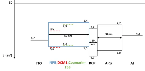
Having all this information, a theory regarding the whole device operation can be proposed. Figure 14 shows the energy levels of all materials for a more efficient analysis about the device operation. The LUMO levels of both dyes are below NPB’s, which allows for an easy trapping of electrons, first from NPB to C153 and after to DCM1, all three HOMO levels are in similar energy levels meaning that holes can easily hop between them.
Figure 14 – Energy levels of all layers constituent of the devices (table 1).
Figure 15 shows all the steps that result in the main emission seen in figure 9 for the proposed theory following a carrier trapping behavior as described in chapter I, section 2.1. If the probability of electrons falling directly from the electrodes into the LUMO levels of both DCM1 and C153 is low, an indirect transition to the dyes through non-radiative transitions is expected. Considering first the interaction NPB-DCM1 (figure 15a), electrons fall from NPB’s LUMO into the excited levels of DCM1. Here, the probability of radiative transition is higher than the non-radiative to lower excited levels
resulting in the emission through them – at higher energies – and not through its LUMO. Raising its
concentration, there’s an increase of electrons hopping to DCM1, promoting radiative transitions of its lower excited levels, hence the redshift in the emission. Considering C153 (figure 15b), it serves as a facilitator of electron transition, allowing electrons to hop easier to DCM1, stabilizing the emission i.e. allowing for the energy levels of DCM1 to saturate more rapidly (the use of low concentrations allows to do so) and so, the device stability is achieved. C153’s non-radiative transition has higher probability over the radiative one at this blend configuration. At low DCM1 concentrations (figure 15c), C153’s emission is promoted similarly to DCM1’s (emission of the excited levels instead of its LUMO) as a result of the decrease of the amount of electrons that transit in a non-radiative way to DCM1.
Figure 15 – Active layer operation. When electrons are injected, they channel to DCM1 in a non-radiative way
without C153 (a) or when C153 is added (b) resulting in the emission of light through DCM1. When its concentration is decreased, the emission of C153 (c) is promoted resulted in the increase of the correspondent peak.
This electrostatic nature of the electrons, or the result of the electric field application for the saturation of dopants, appears to have a more significant importance in the device operation opposite to the energy transfer mechanisms. Either there’s no spectral overlap between the absorption of the dyes and the emission of NPB, or if there is, it is somewhat irrelevant to the emission. Finally, the Förster transition cannot be excluded though given the low dopant concentration which results in a distance between molecules far above the Förster distance, it is possible to assume that is negligible. A Photoluminescent Excitation (PLE) spectrum would allow for a bigger understanding on this entire behavior and, though it was conducted, the results were inconclusive. The same analysis could also be done in solution but the bathochromic shift would mislead the final result. [49]
3. Optoelectronic Characterization
The optoelectronic characterization offers details regarding the viability of an OLED for its general application. It shows how the device operates over its entire regime, its values of brightness and gives great insight on device efficiency, providing information on how to proceed in improving such devices. In this matter, the JVL curves were taken from the set of devices – figure 16.
Though similar in structure, devices I1, I2 and I3 show relative differences in terms of electro-optical behavior. Device I3 (warm white) shows the best results in terms of current density and brightness maximum with 250 A/m2 and 160 Cd/m2 respectively. This can be a result of the increase of DCM1 with its emission promoted, increasing its brightness value. Although the maximum brightness was relatively lower, it is still in the same order of magnitude when compared to the work
24 done prior to this project. [48] Similarly, I1 (cool white) appears next (J~325 A/m2 and L~120 Cd/m2)
where the less efficient emission increase of C153 and general decrease of the emission of DCM1 may be the main responsible for these values. I2 (barrier limit white) has the worst values of the three. The main explanation falls exactly between the other two. This is a barrier limit, both the emissions of C153 and DCM1 are not being promoted in order to produce the color required. Here, the non-radiative transitions appears to be more competitive for such concentrations. These devices could not be compared to other reports in the literature due to the non-use of an integrating sphere (which would show how much light is being emitted from all angles) though a measurement was conducted using the same equipment on an LED monitor. The luminance value obtained was 180 Cd/m2 which is close to the 160 obtained for I3. Also, for all kind of devices, it is not possible to confirm if the molecules all evaporated in the same way, even though the conditions were similar which means that, structurally they can be somewhat different (resulting in a different electrical interaction in the EML having, therefore a direct effect on the device operation).
Figure 16 – JVL curves for devices I1, I2 and I3. The Luminance was taken without background light to reduce
ambient effects.
In terms of applied voltages, though devices I1 and I3 start emitting1 at around 20 V, I2 starts at around 17 V, which may confirm the theory that the structural deposition and/or electrical carrier dynamics throughout Host:Guest may have had an important role here. All devices were put to a limit voltage to understand their behavior. For I2 this resulted in a saturation regime at around 27 V for around 100 cd/m2 while I1 and I3 didn’t show saturation, giving the relative high threshold voltages.
All devices start operating at a significantly high voltage. Of course, when general lighting is concerned, these values must be reduced, but care must be taken because this is not an optimized structure (it was not the objective of this work) so a further study must be conducted to improve carrier injection and decrease the operating voltage. Also, the resistivity of the ITO film is extremely important
for the injection of holes and, in this case, the ITO films had relatively high resistivity values (30-60
Ω/sq) having a direct effect in the threshold voltage.
Figure 17 – a) log(IV) curves for the device I3 displaying the ohmic and SCLC regions. The curve’s slope is an evidence of a deep trap behavior (m>2). b) Efficiency dependence with voltage of device I3 for an OLED with
emission area of 25 mm2.
From the JVL curves, it is possible to gather information regarding the trapping dynamics (section 1.2.2.) – figure 17a. Here, only device I3 was considered giving the previously presented results. Right below the operating voltage, current increases linearly, typical of an ohmic behavior where a small contribution of injected carriers is visible (m~2). Upon entering SCLC, i.e. VΩ~12 V, the slope
of 14 (>2) is clear evidence of a deep-trap behavior which follows the proposed theory. Given that the device requires such high applied voltages, the value of VTFL could not be determined since it disrupts before hitting it.
Finally, the JVL curves can also give a better understanding on the viability of the operating mechanisms, i.e. the device efficiency 𝜂𝐿𝑉 (equation 4.1) – figure 17b.
𝜂𝐿𝑉=𝐿𝐽 =𝐿𝐴𝐼 (4.1)
where A is the area. From this data, assuming an emissive area, A=25 mm2 (figure 8-h), the biggest efficiency obtained was 1.1 cd/A for 25V (J=11.17 A/m2), a low value when compared to other devices (Chapter I section 1.3.). The main difference comes from: 1 - the theoretical 25% efficiency in harvesting the singlet excitons, 2 – only the emission at normal angle was considered (no integration was performed) and 3 - the non-optimized structure of the device. This optimization can include:
Thickness studies meaning how well a layer’s thickness can improve the injection/blockage/transport of carriers. [50]
Plasma treatment of the ITO substrate for work function control. [51]
26 Cathode replacement. Studies showed that the use of Calcium2 passivated with a thin layer of
Al can improve the electrode’s ability to inject electrons to the organic layers given its
reasonably low work function. [3]
Addition of injection layers such as PEDOT:PSS and/or Lithium Fluoride for holes and electrons, respectively that would increase the charge injection. [52]
A stepwise structure for the carriers to provide a pathway with low energy barriers between the electrodes and the organic layers. [53]
Still, this value is closer to other reports at a lower complexity and without integration [28], [45], [54] and actually higher than the ones obtained for the same structure without C153. [48] Though this was not the focus of this project, one thing to have in mind when improving it is the need to find a trade-off between the thickness of the device, the correspondent electric field (which will have a direct effect on the charge mobility) and the device’s complexit accordingly to its main application. To see
the I1 and I2’s trapping dynamics and efficiency values, please consult appendix 4. 4. a.c. analysis
4.1. Impedance Spectroscopy (IS)
With the aid of IS (appendix 5) one, in principle, can construct the equivalent circuits and thereby obtain more insights about the operation of the materials, interfaces and devices. At 0 V dc, the device is typically in its ohmic regime so figure 18a shows the Capacitance and the Dielectric loss dependence with frequency.
Figure 18 - a) Capacitance and dielectric loss curves for the device at 0 V dc typical for the ohmic regime. b) Cole-Cole plot, i.e. the dielectric loss as a function of the capacitance for the same device. Following a model described in the inset with a parallel RC for R1=110 Ω and C1=8.75 nF, a simulated curve was drawn showing a good fitting can be obtained for this model.
2 Calcium is extremely sensitive to environment so it needs to be encapsulated prior to the characterization.