Operational stability of solution based zinc tin oxide/SiO2 thin film transistors under
gate bias stress
Asal Kiazadeh, Daniela Salgueiro, Rita Branquinho, Joana Pinto, Henrique L. Gomes, Pedro Barquinha,
Rodrigo Martins, and Elvira Fortunato
Citation: APL Materials 3, 062804 (2015); doi: 10.1063/1.4919057 View online: http://dx.doi.org/10.1063/1.4919057
View Table of Contents: http://aip.scitation.org/toc/apm/3/6
Published by the American Institute of Physics
Articles you may be interested in
Role of oxygen vacancies on the bias illumination stress stability of solution-processed zinc tin oxide thin film transistors
Applied Physics Letters 105, 023509 (2014); 10.1063/1.4890579
Optical and electrical properties of amorphous zinc tin oxide thin films examined for thin film transistor application
Journal of Vacuum Science & Technology B: Microelectronics and Nanometer Structures Processing, Measurement, and Phenomena 26, 495 (2016); 10.1116/1.2839860
Solution-processed zinc–tin oxide thin-film transistors with low interfacial trap density and improved performance
Applied Physics Letters 96, 243501 (2010); 10.1063/1.3454241
Bias-stress-induced stretched-exponential time dependence of threshold voltage shift in InGaZnO thin film transistors
Applied Physics Letters 93, 093504 (2008); 10.1063/1.2977865
Origin of threshold voltage instability in indium-gallium-zinc oxide thin film transistors
Applied Physics Letters 93, 123508 (2008); 10.1063/1.2990657
Bias stress stability of indium gallium zinc oxide channel based transparent thin film transistors
Operational stability of solution based zinc tin oxide/SiO
2thin film transistors under gate bias stress
Asal Kiazadeh,1,2Daniela Salgueiro,1Rita Branquinho,1Joana Pinto,1 Henrique L. Gomes,2,3Pedro Barquinha,1Rodrigo Martins,1
and Elvira Fortunato1
1CENIMAT/I3N Departamento de Ciência dos Materiais, Faculdade de Ciências e Tecnologia (FCT), Universidade Nova de Lisboa (UNL), and CEMOP/UNINOVA,
2829-516 Caparica, Portugal
2FCT, Universidade do Algarve, Faro, Portugal 3IT-Instituto de Telecomunicações, Lisbon, Portugal
(Received 24 February 2015; accepted 13 April 2015; published online 23 April 2015)
In this study, we report solution-processed amorphous zinc tin oxide transistors exhibiting high operational stability under positive gate bias stress, translated by a recoverable threshold voltage shift of about 20% of total applied stress voltage. Under vacuum condition, the threshold voltage shift saturates showing that the gate-bias stress is limited by trap exhaustion or balance between trap filling and emptying mechanism. In ambient atmosphere, the threshold voltage shift no longer saturates, stability is degraded and the recovering process is impeded. We suggest that the trap-ping time during the stress and detraptrap-ping time in recovering are affected by oxygen adsorption/desorption processes. The time constants extracted from stretched expo-nential fitting curves are≈106s and 105s in vacuum and air, respectively. C2015
Au-thor(s). All article content, except where otherwise noted, is licensed under a Creative Commons Attribution 3.0 Unported License.[http://dx.doi.org/10.1063/1.4919057]
Solution based amorphous oxide semiconductors (AOSs) provide an innovative and low-cost processing technology for thin-film transistors (TFTs).1–4 In order to exploit them into practical
circuits, it is important to assure that their electrical performance is stable under the required work-ing conditions. One of the sources of instability is related with the threshold voltage shift (∆Vth)
when the TFT is operated under constant gate voltage. The phenomena known as gate-bias-stress are common to all TFT technologies, including amorphous oxide TFTs.5–7This instability is related
with surface states of the dielectric which trap charge carriers and shield the externally applied gate-voltage. In the particular case of oxide semiconductors, oxygen adsorption/desorption pro-cesses are also enhanced by an externally applied electric field, contributing to increase instability.8 In spite of all efforts to mitigate this effect, the problem has not been yet properly solved. In fact, even for high quality thermal SiO2 typically used in test structures for performance evaluation of
thin film semiconductors, it is not possible to assure an entirely perfect interface between dielectric and semiconductor. Previously, amorphous oxides using SiO2as dielectric suffer from a pronounced
∆Vth, with time constants (τ) of 104-105s.6,7,9Here, we show evidences of intrinsically more stable
solution-based zinc tin oxide (ZTO) TFTs from studying the time and temperature dependence of bias stress and recovering process. We propose that this enhanced stability is promoted by a defect passivation or neutralization of the SiO2 surface and consequently reducing the number of traps.
We suggest that this passivation is brought out during the thin film fabrication process of the ZTO solution.
The TFTs are produced in a staggered bottom-gate, top-contact structure. Zinc nitrate and tin chloride-based precursors are used to prepare a ZTO solution which is then spin coated on top of a 100 nm thick thermal SiO2on Si substrate. The film is annealed at 350
◦
C in air during 30 min. Next, Al source and drain electrodes (70 nm thick) are e-beam evaporated on top of the annealed ZTO film with typical channel width (W) and length (L) of 1400 µm and 100 µm, respectively
062804-2 Kiazadehet al. APL Mater.3, 062804 (2015)
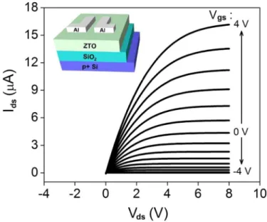
FIG. 1. Output characteristic of the solution based ZTO TFTs on thermal SiO2. The inset shows the ZTO-SiO2TFT structure.
(W/L=14). Patterning is obtained via shadow masks. Figure1 shows the typical output charac-teristic of the device. The schematic of device structure is shown in the inset of this figure. For the mobility µn, the value of the field-effect mobility atVds=1 V is chosen. The subthreshold
swing (SS) is taken as the minimum value ofd(log(Ids)/(Vgs))−1. Typical values for the as-fabricated
devices areVth=−3.1 V,SS=0.35 V/dec, andµn=2.5 cm2/V s at room temperature.
During the positive gate-bias stress (PBS) experiment, all TFTs are biased with a constant gate voltage while source and drain are grounded. After a prefixed time, the bias stress is interrupted and the gate voltage (Vgs) is swept atVds=1 V to measure theIds-Vgscharacteristics of TFT. Stress
measurements are performed in air and under vacuum (10−5millibars, leaving the device at this
pressure for 1 h prior starting the stress experiment) under dark condition. To overcome the problem of non-linearity of transfer characteristics,Vthis taken as the voltage corresponding toIds=1 nA.
PBS displaces the transfer curves to the positive direction. The∆Vthoccurs toward the applied stress
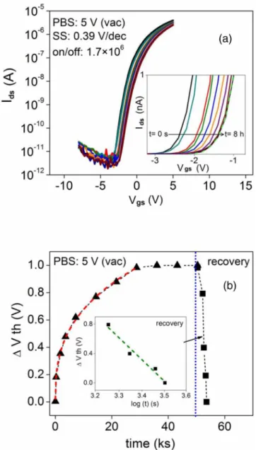
voltage and is continuously shutting down the drain-source current. Figure2(a)shows the shift of the transfer curves under constantVgs=5 V in vacuum. Interestingly, PBS in vacuum results into
threshold voltage displacement during 8 h with∆Vthsaturating after≈1 V shift over this period. The
time dependence of∆Vthcan be well fitted by a stretched-exponential equation as below,
∆Vth=V0
1−exp
− (t
τ )β
,
wheret is the stress time,V0=|∆Vth| at the infinite time, βis the dispersion parameter which is
related to the degree of barrier energy dispersion, andτ is the time constant. TableIshows all the fitting parameters values in different PBS conditions.
In order to get further insight into the physical mechanism of the gate-bias stress, the kinetics of the threshold voltage recovering process is also monitored while the device is kept unbiased under dark conditions. The stress and recovering times are compared in Fig.2(b). The recovering time is fast <1 h, and Vth shift is linearly proportional to the logarithmic time, as observed in
the inset of Fig. 2(b)supporting charge detrapping as the dominant mechanism. The fast device recovery is technologically relevant and to the best of our knowledge, has not been reported so far. The observed behavior can be interpreted in terms of a trap model. The fact that∆Vthreaches
saturation shows that the number of states or defects available is limited. During stress time, the trap filling rate is dominated by the number of defects or available sites (Nt).∆Vthis then given as
∆Vth=eNt/Cox, whereCoxis the capacitance of the gate dielectric andeis the elementary charge.
FIG. 2. (a) Transfer characteristics of ZTO-SiO2TFT at Vds=1 V during gate bias stress with Vgs=5 V, operating in vacuum.
The inset shows the current level at 1 nA. (b) Threshold voltage shift as function of time in vacuum. Red short dashed lines are fitting curves with standard stretched exponential time dependence equation. The green dashed line shows Vthshift is
linearly proportional to the logarithmic time.
states available; therefore at a long enough stress time, all defect states will be eventually filled lead-ing to threshold voltage saturation. It is difficult to assess if the saturation of the threshold voltage is caused by trap exhaustion or alternatively by a competing trap filling/emptying mechanism. At long stress times, the backward (trap emptying) reaction eventually becomes faster than the forward reaction (trap filling). This stops further change in threshold voltage after a certain period of time. As a result, instantaneous threshold voltage shift becomes virtually zero.
Figure3shows the temperature dependence of the threshold voltage shift within the stress time. The time dependence of∆Vthunder stress is fitted by a stretched-exponential equation. The inset of
Fig.3shows thatτis thermally activated by fitting the data to the following equation:
τ=τ0exp(Eτ/kT),
062804-4 Kiazadehet al. APL Mater.3, 062804 (2015)
TABLE I. Stress condition at different temperature, threshold voltage shift∆Vth, time constantτ, dispersion parameterβ, and recovery time.
Stress condition T (K) ∆Vth(V) τ(s) β Recovery
PBS (air, 14 h) 295 3.44 1.5×10⁵ 0.52 ∼7days PBS (vacuum, 8 h) 295 0.98 5.6×10⁶ 0.36 53 min NBS (air, 6 h) 295 −2.23 8.2×10⁶ 0.25 ∼30 min NBS (vacuum, 6 h) 295 −2.15 9.0×10⁶ 0.28 ∼30 min PBS (vacuum, 6 h) 345 1.20 1.9×10⁶ 0.43 <20 min PBS (vacuum, 6 h) 395 1.49 6.3×10⁵ 0.51 <20 min PBS (vacuum, 6 h) 420 1.63 4.4×10⁵ 0.51 <20 min
on other semiconductor technologies using SiO2as a gate dielectric, supporting the view that this
defect is not intrinsic to ZTO but instead related with the SiO2surface.7,9
Under the presence of ambient atmosphere (295 K, 1 bar) during PBS process, the ZTO-TFT stability is severely degraded. However, the presence of oxygen does not affect the negative bias stress (NBS) instability. The fitting parametersβandτare approximately equal for NBS measure-ments under vacuum and in the presence of atmosphere as shown in TableI.
Fig.4(a)shows the typical electrical characteristics of the device under a gate-bias stress of 5 V in ambient atmosphere. The time dependence of∆Vthassociated with fitting plots is shown in Fig. 4(b). The time constant (τ=105 s) is now one order of magnitude lower than the one measured in vacuum (τ=106s). Higher value ofτ indicates that at a particular temperature, the course of threshold voltage shift persists longer and the operational stability is enhanced. In this respect, τ can be used as a figure of merit to quantify operational stability. The value ofβ(β=0.52) is higher in vacuum than in air (β=0.36). This means that the distribution of energy barriers or trap sites becomes broader when oxygen adsorption occurs. Furthermore, theVthdoes not saturate, suggesting
that more defect states become available in the presence of atmosphere. Most relevant, the ability of the device to recover the originalVthis severely impeded, being the recovering time now more than
106s. This time contrasts with the behavior in vacuum where a few minutes under unbiased
condi-tions are enough to fully recover the originalVth. The recovering fitting shows the time constant of
5.5×10⁴s. This value is one order of magnitude smaller than trapping time during PBS in air. It
FIG. 4. (a) Transfer characteristics of ZTO-SiO2TFT atVds=1 V during gate bias stress withVgs=5 V, operating in air. (b) Threshold voltage shift as function of time on a logarithmic scale and the recovery processes in air. The red dashed lines are fitting curves with stretched exponential equation.
supports that the recovering process is not only charge detrapping process but also the oxygen ion desorption from the channel surface contributes in the recovering mechanism. Nevertheless, theβis the same for stress/recovery process indicating the similar barrier energy dispersion of trap sites.
The fact that the threshold voltage can shift faster in air than in vacuum has been reported by a number of authors and tentatively explained by several mechanisms.10,11The new finding reported
here is that for solution based ZTO, the presence of atmospheric species impedes the fast recovering of the Vth observed under vacuum conditions. In order to explain this behavior, we propose that
oxygen species adsorb to the ZTO back channel exposed surface. The effect of external electric field which can induce the chemisorption of oxygen on zinc oxide thin film has been already reported in 1968. A field which brings electrons to the surface would favor increased oxygen adsorption.8
Ox-ygen is a weak electron acceptor and removes free electrons from the bulk ZTO leading to overall reduction in the free carrier concentration. Therefore, it results in a depletion layer on the surface and increase of threshold voltage. During the recovering time when the device is kept unbiased, it is difficult to remove the oxygen molecules without any driving force. Therefore, theVthhardly
062804-6 Kiazadehet al. APL Mater.3, 062804 (2015)
gate bias stress experiment in air: (i) surface dielectric states trap electrons and shield the external gate bias, and (ii) adsorbed oxygen layer on the top exposed ZTO surface captures free carriers from ZTO. The two effects add to each other contributing to a further increase in threshold voltage shift in air.
In summary, we have shown that solution based ZTO-TFTs are highly stable in vacuum. The threshold voltage shift saturates in a time scale of 104 s. Furthermore, when the TFTs are kept unbiased, they exhibit a remarkable fast recovering behavior of the threshold voltage shift. We attributed this high operational stability to a passivation/neutralization of SiO2surface defects
occurring during the drying/annealing of the ZTO solution. Saturation of the threshold voltage shift may arise because the number of traps is finite, or alternatively because the internal field caused by the immobile trapped carriers will lead to a balance between trap filling and emptying. The presence of atmospheric species eliminates the ability of the stressed device to restore the original threshold voltage. We propose that a negatively charged oxygen layer is depleting the ZTO bulk from free carriers and impedes theVthto be restored to original values. Encapsulation of the devices
should prevent the interference of oxygen species and diminish this effect. The deposition of semi-conductor layers under vacuum should in principle lead to a better control of impurity densities, interestingly the results reported here suggest that solution based amorphous oxides can intrinsically passivate the dielectric surface and lead to highly stable devices.
This work is funded by FEDER funds through the COMPETE 2020 Programme and Na-tional Funds through FCT–Portuguese Foundation for Science and Technology under the Project Nos. UID/CTM/50025/2013 and EXCL/CTM-NAN/0201/2012 and the European Communities 7th Framework Programme under grant agreement ICT-2013-10-611070 (i-FLEXIS project).
1R. Branquinho, D. Salgueiro, A. Santa, A. Kiazadeh, P. Barquinha, L. Pereira, R. Martins, and E. Fortunato,Semicond. Sci.
Technol.30, 024007 (2015).
2L. Jun seok, K. Young-Jin, and C. Woon-Seop,J. Korean Phys. Soc.59, 3055 (2011). 3S.-J. Seo, C. G. Choi, Y. H. Hwang, and B.-S. Bae,J. Phys. D: Appl. Phys.42, 035106 (2009).
4R. Branquinho, D. Salgueiro, L. Santos, P. Barquinha, L. Pereira, R. Martins, and E. Fortunato,ACS Appl. Mater. Interfaces
6, 19592 (2014).
5Y. Jeong, C. Bae, D. Kim, K. Song, K. Woo, H. Shin, G. Cao, and J. Moon,ACS Appl. Mater. Interfaces2, 611 (2010).
6J. S. Park, W.-J. Maeng, H.-S. Kim, and J.-S. Park,Thin Solid Films520, 1679 (2012). 7J. M. Lee, I. T. Cho, J. H. Lee, and H. I. Kwon,Appl. Phys. Lett.93, 093504 (2008).
8S. A. Hoenig and J. R. Lane,Surf. Sci.11, 163 (1968).
9M. E. Lopes, H. L. Gomes, M. C. R. Medeiros, P. Barquinha, L. Pereira, E. Fortunato, R. Martins, and I. Ferreira,Appl.
Phys. Lett.95, 063502 (2009).