INTERNATIONAL JOURNAL OF SCIENTIFIC & TECHNOLOGY RESEARCH VOLUME 4, ISSUE 01, JANUARY 2015 ISSN 2277-8616
229 IJSTR©2015
www.ijstr.org
Surface Morphology And Photoluminescence
Properties Of A-GaAs:Se Detector
Hussein Kh. Rasheed, Dhuha Imad
Abstract: (GaAs:Se) films with thickness 0.5 m have been prepared by flash evaporation technique on glass substrate under vacuum of 10-5mbar. These films have been annealed at different temperatures ( 373 , 473)K. The surface morphological characteristics by atomic force microscope (AFM). The roughness was decrease with increasing annealing temperature for amorphous film but start upward when the films crystallized. The grain size increases with increasing annealing temperature upto temperatures (373,473) K . The spectral response of GaAs:Se was studied. The values of responsively, specific detectivity and quantum efficiency increases with increases annealing temperature but NEP decreases with increases annealing temperature. The Photoluminescence peak of a-GaAs:Se films located at 832.215, 829.87 and 827.538 for temperature at RT,100 and 200 oC which corresponding to an energy gap 1.49 , 1.494 and 1.498 eV respectively. This may be associated which that the electron in bottom of conduction band recombines with hole in the valance band.
————————————————————
1
I
NTRODUCTIONIII-V semiconductors are commonly used in the fabrication of optoelectronic devices and its electron effective mass is only 1/16 of that of Si, consequently with higher mobility of electrons. This makes GaAs a prospective candidate for the production of future integrated circuits despite its technologically more elaborate processing[1]. An interesting feature of III-V compounds is relationship between band gap and composition which gives device designer. These compounds have direct transitions, the absorption coefficient rises steeply at the band edge to values of 104 cm-1 or more [2] . Many structure and morphological studies have been made of on amorphous silicon [3] two phase and columnar structure models [5,6]had been used to interpret many of the experimental results. Few results can be found in the literature on III-V amorphous materials and then morphologies [7-9]. In addition to high optical and electrical quality of the films, the heavily doped epitaxial film for optoelectronic device applications require mirror smooth surface morphology. The mirror smooth surface morphology and specific concentration of impurity in GaAs by MOCVD can be obtained by controlling the growth temperature. The heavy doping affects the density of states, carrier mobility, absorption, band structures, luminescence properties and hence the device performance [10,11]. Also, the high doping affects the band gap shrinkage and by a band tail extending into the gap. In the hetero junction-based devices, the band gap shifts due to heavy doping result in valence and conduction band discontinuity of the heterojunction interface [12]. Low temperature photoluminescence (LTPL) spectroscopy is a common characterization technique for investigating the band structures of GaAs at high doping levels. band gap shrinkage due to heavy doping is a well-known phenomenon in III–V compound semiconductors ,particularly observed in GaAs by PL spectroscopy[13 –20]. The luminescence properties are dependent on the growth conditions (methods), doping concentrations, impurity species, growth temperatures, etc.
2
E
XPERIMENTAL WORKGaAs powder (99.999%) doped with 1% Se as a thin films were prepared using an Edwards high vacuum coating unit model E 306A with an arrangement for flash evaporation method under vacuum 10-6 mbar. The substrate were glass which were cleaned with chromic acid, alcohol and in ultrasonic cleaner. The substrate was placed at a distance 15cm from the evaporator ,molybdenum was used as a boat source, the mean film deposition rate 3.3A/sec and the film thickness was measured by interference method . These film was annealed at a different temperature (373,473)K. The spectral measurements has been carried out at room temperature by using the heterojunction , which consists of UV–NIR source in the region (300–1000) nm, D.C. power supply, monochrometer type (SPEX – minimate) in the range (400–1000) nm. The photoluminescence spectra of the GaAs suspension at different preparation condition at room temperature in quartz cell with 1cm optical path, were measured using SL-174 (ELICO) SPECTRO FLUOROMETER,150 watt Xenon Arc lamp,(EX and Em) from (200-900)nm, using 4.49eV as wavelength excitation.
3
R
ESULT AND DISCUSSION3-1MORPHOLOGY PROPERTIES OF GaAs:Se/C-SI THIN FILM Figure (1) show the structure of GaAs:Se thin films that have been deposited on glass substrates and annealed at RT ,373 and 473 K with thicknesses 0.5 µm. The surface morphology of the GaAs:Se films as observed from the AFM micrograph confirms that the grains are uniformly distributed. We can notice that GaAs:Se films deposited at room temperature and annealed to 373K are amorphous while the films annealed to 473K are crystalline in nature . Table (1) shows the value of average roughness and average grain . It was observed from this table that the average roughness and the average grain size value decreases with increasing the annealing temperature.
__________________________
Hussein Kh.Rasheed, Department of physics,college of science,university of Baghdad.Iraq
INTERNATIONAL JOURNAL OF SCIENTIFIC & TECHNOLOGY RESEARCH VOLUME 4, ISSUE 01, JANUARY 2015 ISSN 2277-8616
230 IJSTR©2015
www.ijstr.org
Fig1 . Atomic force microscopy image for GaAs film doped with 1% Se depositedon Si wafer at different
annealing temperatures
Figures (2): PL spectrum of GaAs :Se films on glasssubstrate
TABLE (1):
THE VALUE OF AVERAGE ROUGHNESS, RMS AND AVERAGE GRAIN
SIZE FOR GAAS FILM DOPED WITH 1%Se AT THICKNESS 0.5ΜM.
3-2PHOTOLUMINESCENCE SPECTRA OF A-GAAS:SE FILMS The dependence of PLspectra of a-GaAs:Se films on annealing temperature was shown in figure (2). The PL peak located at(832.215),(829.87) and(827.538) for (RT,100 and 200)oCwhich corresponding to an energy (1.49),(1.494) and(1.498) eV respectively. This may be associated to the electron in bottom of Ecrecombine with hole in the Ev This behavior can beinteroperate in term the improvement the
crystal structure with increase annealing temperature as well as reduction the localized state for mobility gap as described by many Authors such as Brodsky.Also we can see from this figure (2)the peaks shifts toward the start wavelength with increases the annealing temperature .
3-3 SPECTRAL MEASUREMENTS FOR GaAS:Se/C-SI
HETEROJUNCTION
3-3-1SPECTRAL RESPONSIVITY
Spectral responsivity(R) is the most important parameter by which the range of hetrerojunction operation can be determined. Fig.(3) shows the variation of the spectral responsivity with the wavelength for GaAs:Se heterojunction at thickness 0.5µm at R.T and annealing temperatures (373 and 473) K. The spectral responsivity increases with increasing of the annealing temperature due to increasing of the annealing temperature due to increasing of the photocurrent, also because of the increasing the efficiency to separate the electron-hole pairs by the internal electric field. We can see from table (2) that the peaks of R are shifted to shorter wavelength as the annealing temperature increases due to the increase of the optical energy gap.
Fig3.the variation of responsivity as a function of wave length for GaAs:Se hetrojanction at a different annealing
temperatures
3-3-2NOISE EQUIVALENT POWER
The noise equivalent power (NEP) values shown in Fig.(4) and Table (2) for GaAs:Se heterojunction at thickness 0.5m at R.T and annealing temperatures (373 and 473) K. We can observe that the minimum NEP occurs when R has the maximum value.. Also we can notice from this figure and Table (2) that NEP decreases with increasing of annealing temperatures.
Fig4.the variation of NEP as a function of wave length for GaAs:Se hetrojanction at a different annealing temperatures
3-3-3THE SPECIFIC DETECTIVITY
The variation of specific detectivity (D*) as a function of wavelength for GaAs:Seheterojunction0. 5m at R.T and Ta
(K)
Average diameter (nm)
Average roughness (nm)
Peak – Peak(n m)
RT 128.11 0.885 5.13
373 103.46 0.368 2.22
INTERNATIONAL JOURNAL OF SCIENTIFIC & TECHNOLOGY RESEARCH VOLUME 4, ISSUE 01, JANUARY 2015 ISSN 2277-8616
231 IJSTR©2015
www.ijstr.org annealing temperatures (373 and 473) K is presented in Fig.(5). It is obvious that the D* value increases with increasing annealing temperatures due to the decrease of NEP.
Fig. 5 The variation of specific detectivity as a function of wavelength for GaAs:Se heterojunction at different
thicknesses and annealing temperatures
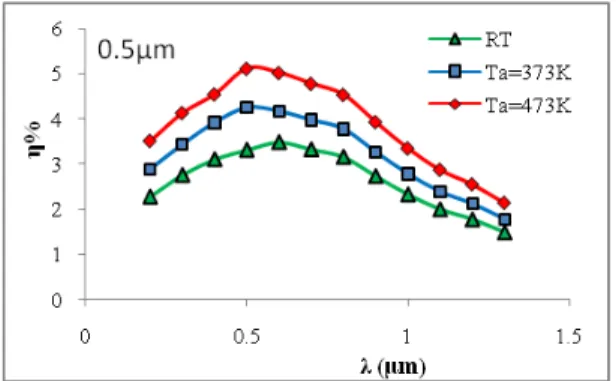
3-3-4QUANTUM EFFICIENCY
The quantum efficiency (η) is a very important parameter in the photovoltaic devices which is recognized by the optoelectronic effect. It represents the ratio between the numbers of generated electrons in the heterojunctions to the number of incident photons on the effective area of the heterojunctions. η is related to the change of the spectral responsivity as shown in Fig.(6) and Table (2) due to the same reasons mentioned earlier for responsivity.
Fig. 6The variation of quantum efficiency as a function of wavelength for GaAs:Se heterojunction at different annealing
temperature
TABLE(2)
VALUES OF PEAK ,R,%,NEP AND D* AT DIFFERENT ANNEALING
TEMPERATURE
CONCLUSION
The surface morphological characteristics by atomic force microscope show a decrease in roughness and grain size with increasing annealing temperature. The PL peak located at(832.215),(829.87) and(827.538)for (RT,373 and 473)K corresponding to an energy (1.49),(1.494) and(1.498)eV.The spectral response of GaAs:Se heterojunction exhibits the combined effect of photogeneration in the Si side and GaAs side of the heterojunction. The responsivity, specific detectivity and quantum efficiency increasing with increasing of annealing temperatures .Noise equivalent power decreases with increasing of annealing temperatures.
R
EFERENCES[1] S. Kayali, J. Ponchak and R. Shaw "GaAs MMIC Reliability Assurance Guide Line for Space Applications" NASA 1996. http/www.Google.com.
[2] R.K. Willardson and Albert C. Beer "Semiconductor and Semimetal" vol 2, Academic press ,inc. London LTD 1975
[3] J.C.Knights,in: "the physics of hydrogenated amorphous silicon",ed.J.D.Joannopulos and G.Lucovsky,Topics in Applied physics, Vol.55(springr,Berlin,1981)p.5
[4] W.Paul and D.A. Anderson,solar Energy Mater .5 (1981)229.
[5] J.C.Knights and R.A.Lujan,appl.phys.Lett.35(1979)244
[6] R.Messier and R.C.Ross,J,Appl.phys.53 (1982)6220
[7] L.Alimoussa,H.Carchano .A.Fassi-Fihri,F. Lalande and R.Loussier,J.PhysC1-(1982) 341
[8] A.Gheorghiu,T.Rappenau,s,Fisson and M.L they, thin solid films 120 (1984)491
[9] R.Murri,f.Gozzo,N.pinto ,L.Schiavulli,c,DeBlasi and D.Manno,J.Non-cryst.solids 127(1991)12.
[10]C.R Absernathy, F. Ren, P.W. Wisk, S.J. Pearton, R Esagui,Appl. Phys. Lett. 61 (1992) 109
[11]L.J. Guido, G.S. Jackson, D.C. Hall, W.E. Plano, N. Hollonayak,J.Appl Phys. Lett. 52 (1988) 522.
[12]J.A. Silberman, T.J. de LyonJ.M. Woodall, Appl. Phys. Lett. 58(1991) 2126.
[13]D. Olego, M. Cardona, Phys. Rev. B. 22 (1980) 886. Ta
(K)
peak
(m)
R(A/W) % NEP10 -9
(Watt)
D*108 (cm.Hz1/2.W
-1
)
RT 0.8 0.020 3.479 1.82 3.85
373 0.8 0.024 4.257 1.43 4.89