Pedro Gil Dias Trigo
Licenciado em Ciências de Engenharia de Micro e Nanotecnologia
Oxide transistors produced by Combustion
Synthesis: Influence of the PVP on the
properties of the insulator
Dissertação para obtenção do Grau de Mestre em Engenharia de Micro e Nanotecnologia
Orientador: Doutora Rita Maria Mourão Salazar
Branquinho, Prof. Auxiliar, FCT-UNL
Júri:
Presidente: Doutor Hugo Manuel Brito Águas, Prof. Auxiliar, FCT-UNL
Arguente: Doutor Rui Alberto Garção Barreira do Nascimento Igreja, Prof. Auxiliar, FCT-UNL
Vogal: Doutora Rita Maria Mourão Salazar Branquinho, Prof. Auxiliar, FCT-UNL
III
Oxide transistors produced by Combustion Synthesis:
Influence of the PVP on the properties of the insulator
Copyright © Pedro Gil Dias Trigo Faculdade de Ciências e Tecnologia
Universidade Nova de Lisboa
V
Acknowledgements
First, I would like to thank my institution, the Faculty of Science and Technology of the Universidade Nova de Lisboa, and my department, Materials Science, for all the experiences provided over the years with a great academic life, which helped me growing.
Secondly, I would like to send my greatest gratitude to Professor Rodrigo Martins and Professor Elvira Fortunato for their dedication, commitment and hard work on Micro and Nanotechnology course and for offering the best infrastructures and conditions possible in CENIMAT|I3N and CEMOP, which allowed me to do my master thesis with the best possible experience possible with outstanding work conditions
To my supervisor Rita Branquinho with whom I had the privilege to work with, who helped me along these months, even when she had tons of work to do, the patient she had and the new ideas she provided for me to have the best master thesis possible, I want to give her special thanks. I also need to thank the remaining team members who attended the meetings we had, Sofia Ferreira for listening and providing some solvent and Daniela Salgueiro who helped me several times in different matters
To my good friend Emanuel Carlos for many different reasons but above all for being there for me every time I needed him every single time. He taught me many things, many details to succeed and not once did he refuse to listen to my ideas and tell me if whether they were good or bad. Furthermore, he is an amazing guy outside the workplace with whom I had the pleasure to hang out with and share some outstanding moments.
To Alexandra Gonçalves and Sónia Pereira for providing me all the tools needed for my work and to Tomás Calmeiro for obtaining the AFM images of my samples. In that regard, I would like to thank Joana Pinto for obtaining the XRD images and Daniela Gomes for the SEM images of my samples. To professor Luís Pereira for helping me by doing a hybrid mathematic model that I could use in spectroscopic ellipsometry. I would like to thank all the other members who work at the institution for always being present to support me.
To my good friends in Open Space for all the laughs and time we spent together in these last months. I would like to thank Alexandre Fonseca for all the jokes, the time we spent together, the help your kidney provided in my martial arts training and all the laughs after I tackled you almost all games we played together in football.
To my colleague and friend Marco Moreira with whom I had the honor to work. All the car halls I gave you which you repaid with joy and funny moments. We had our struggles but in the end, you were very important for me during my master thesis,
To all my colleagues in the course of Micro and Nanotechnology that accompanied me for all my years. To my deepest friends José Correia, Tomás Vasconcelos, Nuno Bártolo, Miguel Monteiro, Luka Lett and Bernardo Mendes for all the life experiences I will never forget. The jokes, the parties and the laughs that came with it is something that will be with me forever.
VII
Abstract
Solution processing of amorphous metal oxides has been used as an option to implement in flexible electronics, allowing to reduce the associated costs, when compared with vacuum processes. Recent research has been more focused on the semiconductor layer; however, the dielectric layer is equally important since its responsible for the stability and electric performance of the device.
This work aims to evaluate hybrid dielectric thin films, using aluminium oxide and different types of polyvinylpyrrolidone (PVP), both obtained by solution process using solution combustion synthesis (SCS), to study the influence of the amount of organic material used in the insulator layer, as well as to study the influence of the hybrid insulator obtained in oxide thin film transistors (TFTs) using indium-gallium-zinc-oxide (IGZO) and zinc-tin-oxide (ZTO) as semiconductor layer. The insulator layer was obtained using aluminium nitrate nonahydrate and polyvinylpyrrolidone (PVP) with different molecular weights (10000 and 40000) and different percentages as precursor solutions, using urea as fuel and 2-methoxyethanol as solvent.
The best hybrid dielectric was obtained with 0.8 % PVP 40000 (weight per volume), showing a breakdown voltage of 1.1 MV/cm, low density leakage current of 9.6 × 10⁻⁵ A/cm2, capacitance per area of 123 nF/cm2, thickness of 49.35 nm, annealed at 200 °C for 30 minutes. Moreover, the roughness study obtained using atomic force microscopy showed highly smooth surface, resulting in improvement dielectric-semiconductor interface, while still maintaining an amorphous nature. These characteristics allowed this hybrid dielectric, lead to enhanced TFTs electrical properties. The best performing thin films were applied in IGZO TFTs as hybrid dielectrics. The optimized TFTs show good reproducibility with an average mobility of 40.24 ± 1.1 cm2∙V-1∙s-1, subthreshold slope of 0.169 ± 0.012 V∙dec-1, a turn-on voltage of 0.078 ± 0.004 V and a low operating voltage (maximum 2 V).
IX
Resumo
O processamento por solução de óxidos metálicos amorfos tem sido utilizado como opção de implementação em eletrónica flexível, permitindo reduzir os custos de produção associados, quando comparado por processos por vácuo. Investigações recentes têm como foco principal a camada do semicondutor, no entanto a camada do dielétrico é igualmente importante uma vez que é responsável pela estabilidade e performance elétrica do dispositivo.
Este trabalho procura avaliar dielétricos de filmes finos híbridos, utilizando óxido de alumínio e diferentes tipos de polivinilpirrolidona (PVP), ambos produzidos por solução via síntese combustão por solução (SCS), para estudar a influência do material orgânico e quantidade utilizada na camada isolante, tal como estudar a influência do dielétrico híbrido em transístores óxidos de filme fino (TFTs) utilizando óxido de índio-gálio-zinco (IGZO) e óxido de zinco-estanho (ZTO) como camada semicondutora. A camada isolante foi obtida utilizando nitrato de alumínio nonahidratado e polivinilpirrolidona (PVP) com diferentes pesos moleculares (10000 e 40000) e diferentes percentagens em diferentes soluções precursoras, utilizando ureia (U) como combustível e 2-metoxietanol (2-ME) como solvente.
O melhor dielétrico híbrido foi obtido com 0.8% PVP 40000 (peso por volume), por apresentar uma tensão de rutura de 1.1 MV/cm, baixa densidade de corrente de fuga 9.6 × 10⁻⁵ A/cm2, capacitância por área de 123 nF/cm2, espessura de 49.35 nm, recozido a 200 °C durante 30 minutos. Para além disso, o estudo da rugosidade feito pelo microscópio de força atómica mostrou uma superfície altamente lisa, resultando numa melhoria da interface entre o dielétrico e semicondutor, mantendo uma natureza amorfa. Estas características permitiram este dielétrico híbrido obter melhores propriedades elétricas nos TFTs. Os filmes finos com melhor performance foram aplicados em TFTs com IGZO como dielétricos híbridos. Os TFTs otimizados apresentam boa reprodutibilidade com uma mobilidade média de 40.24 ± 1.1 cm2∙V-1∙s-1, subthreshold slope de 0.169 ± 0.012 V∙dec-1, uma tensão de abertura de 0.078 ± 0.004 V e baixa tensão de funcionamento (máximo 2 V).
XI
List of Abbreviation
2-ME – 2-methoxythenol
AFM – Atomic Force Microscopy AlOx– Aluminium oxide
ATR – Attenuated Total Reflectance
CEMOP – Center of Excellence in Microelectronics and Optoelectronics Processes CENIMAT – Centro de Investigação de Materiais
Cf – Capacitance-frequency CV – Capacitance-voltage DC – Direct current
DSC – Differential Scanning Calorimetry DUV – Deep Ultraviolet
EDL – Electric double layer
EDS – Energy Dispersive X-ray Spectroscopy FET – Field effect transistor
FPDs – Flat panel displays
FTIR – Fourier Transform Infrared Spectroscopy GAXRD – Glancing angle X-ray diffraction IGZO – Indium-Gallium-Zinc oxide
IV – Current-voltage
MIS – Metal-Insulator-Metal M-O-M – Metal oxide metal
MOSFET – Metal oxide semiconductor field effect transistor OTFTs – Organic thin film transistors
OV – Oxidizing valence
PEN – Polyethylene Naphthalate PMMA – Poly (methyl methacrylate) PVD – Physical vapor deposition
PVP 1 – Polyvinylpyrrolidone of 10000 molecular weight PVP 2 – Polyvinylpyrrolidone of 40000 molecular weight Rms – Surface roughness (root mean square)
rpm – Rotations per minute RV – Reducing valence
XII TG – Thermogravimetry
U – Urea
UV – Ultraviolet Vis – Visible
XIII
List of Symbols
A – Area
c – Capacitance (F) Cox – Oxide capacitance
CD – Semiconductor depletion capacitance Ct – Total capacitance
d – Insulator thickness ∆E - Conduction band offset Eg– Band gap
ε0– Permittivity of free space (8.854×10⁻¹² F m-1) 𝑔𝑚– Transconductance
h – Hour
IDS– Current between drain and source
IG– Gate leakage current
Ioff– Drain current in the off state
Ion– Drain current in the on state
J – Density of leakage current
k – Dielectric constant of the insulating material L – Channel length
M – Molar min – Minutes q – Charge
SS – Subthreshold slope tA – Annealing time
VDS– Voltage between the drain and source
VGS– Voltage between the gate and source
VHyst– Hysteresis
Von– Turn-on voltage
VT– Threshold voltage
XV
Table of Contents
1 Introduction ... 1
1.1 Solution Combustion Synthesis (SCS) ... 1
1.2 Hybrid Dielectrics ... 2
1.3 Metal-Insulator-Metal (MIS) Capacitors ... 3
1.4 Thin Film Transistors (TFTs) ... 4
2 Materials and Methods ... 7
2.1 Hybrid AlOx/PVP Precursor Solutions Preparation and Characterisation ... 7
2.2 Thin Film Deposition and Characterisation ... 7
2.3 Electronic Devices Fabrication and Characterisation ... 8
3 Results and Discussion ... 9
3.1 Hybrid AlOx/PVP precursor solution characterisation ... 9
3.2 Thin Films Characterisation ... 11
3.2.1 Optical Characterisation ... 11
3.2.2 Spectroscopic Ellipsometry ... 12
3.2.3 Structure and Morphological Characterisation ... 13
3.3 Electrical Characterisation of Hybrid solution based AlOx/PVP capacitors ... 15
3.3.1 Influence of PVP 1 in AlOx capacitors ... 16
3.3.2 Influence of PVP 2 in AlOx capacitors ... 17
3.3.3 Influence of the number of hybrid dielectric layers ... 18
3.4 TFTs Electrical Characterisation ... 20
3.4.1 IGZO TFTs with AlOx/PVP 1 hybrid dielectric ... 20
3.4.2 IGZO TFTs with AlOx/PVP 2 hybrid dielectric ... 21
3.4.3 Influence of the semiconductor layer ... 23
3.4.4 Stability over time of IGZO/AlOx/PVP2 TFT ... 25
3.4.5 IGZO TFTs with AlOx/PVP 2 hybrid dielectric in flexible substrate ... 26
4 Conclusions ... 27
5 Future perspectives ... 29
6 References ... 31
7 Annexes ... 37
Annex A ... 37
Annex B ... 39
Annex C ... 41
Annex D ... 43
Annex E ... 45
Annex F ... 49
Annex G ... 51
XVII
List of Figures
XVIII
XIX
List of Tables
Table 1: Characteristic absorbance peaks and associated vibrational modes of the corresponding
chemical bonds for the spectrum of AlOx/PVP thin film on silicon [54, 55]. ... 12
Table 2: Thickness (nm) of multilayer hybrid dielectric thin films. ... 13
Table 3: Carbon atomic percentage of hybrid dielectrics measured by EDS ... 14
Table 4: Dielectric constant of AlOx and hybrid films of AlOx/PVP 1. ... 17
Table 5: Dielectric constant of AlOx and hybrid films of AlOx/PVP 2. ... 18
Table 6: Dielectric constant of multilayer hybrid films of AlOx/PVP ... 19
Table 7: Characteristic parameters of IGZO/AlOx/PVP 1 TFTs for different concentrations of dielectric annealed at 200 °C. ... 21
Table 8: Characteristic parameters of IGZO/AlOx/PVP 2 TFTs for different concentrations of PVP annealed at 200 °C. ... 22
Table 9: Characteristic parameters of ZTO/AlOx/PVP TFTs for different concentrations of dielectric annealed at 200 °C. ... 24
Table 10: Electrical properties obtained for the hybrid TFT depicted in Figure 3.18. ... 26
Table 11: Valence of all elements and respective reagents. ... 37
Table 12: Thickness of all thin films characterized by ellipsometry. ... 43
Table 13: Dielectric constant (k) of hybrid thin films with high PVP percentage using the capacitance measured at 100 kHz. ... 46
Table 14: MIS structures using hybrid dielectrics from recent research. ... 51
XXI
Motivation and Objectives
Nowadays printed transparent electronics is one of the most promising technologies due to potential applications in several areas. The development of materials with applications in flexible electronics that can be processed by solution is crucial due to the lower cost and the use of less energy by using low processing temperatures [1]. One of the main components in electronic is thin film transistors (TFTs). These devices should have a good performance, reproducibility and reliability to be applied in the industry [2]. In that regard, solution-processed metal oxide TFTs have been studied. The electronic circuits have more small transistors integrated, with the objective of reaching higher performance, more applications and reduce the costs [3–5]. The continuously decrease in the transistors’ size leads to technology issues in the semiconductor industry [6–8], however, the TFTs performance depends also in the dielectric layer, which is responsible for the stability and electrical performance of the devices. Polyvinylpyrrolidone (PVP) is a polymer with good stability, even though it is an organic, transparent and have good insulator properties. Being an organic material, flexibility is one of the many advantages it has, moreover, PVP can be used to fill the porosity created from the oxide formation using the solution combustion synthesis (SCS) [9–11].
By using organic materials and metal oxides with high-k dielectrics, the advantages offered by both materials have attracted considerable attention [12]. So, the development of a hybrid dielectric layer produced by solution is the focus in this master thesis.
1
1
Introduction
During the last decade, oxide semiconductors have been extensively studied regarding their application as channel material in thin film transistors (TFTs) because of their superior electrical properties, such as mobility, uniformity and reasonable electrical stability as compared to amorphous silicon. The possibility of low temperature processing, combined with a wide band gap (Eg) made these devices suitable for transparent and flexible electronics [3, 4]. Unfortunately, most of these high-performance oxide TFTs are usually manufactured using costly vacuum-based techniques. To address these problems, among the various process technologies, solution process has many advantages: not only simple and low cost process, but also good homogeneity and excellent compositional control and high throughput [13–16]. Many of the circuit applications of organic TFTs are not primarily driven by the need for higher device performance but by the compatibility of organic materials with low-temperature processing on non-conventional substrates, such as flexible plastic substrates. Furthermore, solution-processible organic materials are compatible with direct-write printing-based manufacturing techniques that allow to apply distortion compensation techniques to keep accurate layer-to-layer registration on large-area plastic substrates, which exhibit pronounced dimensional changes during device processing [5]. Therefore, solution processes of organic and inorganic materials allow the processing at low temperatures, enabling new possibilities for low cost printable and transparent devices using flexing substrates [14, 17].
The demands for low-cost flexible electronics mentioned earlier led to a remarkable development of solution-based production methods and solution-processed inorganic metal oxide semiconductor materials for high-performance thin-film transistors (TFTs), and such devices have demonstrated competitive results when compared with materials obtained by physical techniques [14, 15, 18]. Still, their poor mechanical properties limit their use in flexible electronics. An option to overcome the limitations of metal oxide dielectrics is to employ polymer dielectrics, but the polymers typically have low dielectric constants as compared to metal oxides, and they usually require large thicknesses as gate dielectrics to avoid high leakage currents. To overcome these problems, hybrid dielectric layers offer a good option by surpassing the inorganic drawbacks, such as mechanical flexibility, and because of the organic material it usually reduces the roughness of the dielectric layer, allowing a better interface between the dielectric and semiconductor [19].
Inkjet-printing, spin-coating, and dip-coating are the main deposition methods for solution-based processes [20, 21].
1.1
Solution Combustion Synthesis (SCS)
Despite most solution processes replaced the vacuum-based processes, the condensation, densification, and impurity removal steps of solution oxide film processing typically require an annealing above 400 °C, which is not compatible with most flexible plastic substrates and carry many risks, such as cracking induced by thermal expansion coefficient mismatch [17, 22].
2
Figure 1.1 shows the relation between the energy required for a conventional reaction to a self-combustion reaction.
Figure 1.1 Comparison of the energy required for a conventional reaction relatively to a self-combustion
one [6].
Recently, the pursuit of environment friendly solvents for electronic applications, such as ethanol and water, is growing [30–32]; however, organic solvents, like 2-methoxyethanol (2-ME), are currently the most used to produce oxide thin films for electronic applications purposes, even though they are toxic solvents, because condensation, densification and impurity removal is required, otherwise and/or an additional annealing process at temperatures above 400 ºC is required [17, 32].
1.2
Hybrid Dielectrics
Over the recent years, various organic devices have been studied, in particular the organic thin film transistors (OTFTs) have been the focus of investigation due to their flexibility, low manufacturing cost, large area fabrication and light height [33–35]. Moreover, their performance over the years has been remarkably improved. Polyvinylpyrrolidone (PVP) and Poly (methyl methacrylate) or PMMA are the most common organic materials used [35, 36].
PVP has been the focus of a wide range of fundamental and application-orientated studies. PVP is hygroscopic and easily soluble in water and organic solvents such as alcohols, and the presence of hydroxyl groups should favour coordination to the metal oxides lattice [36, 37]. Due to these characteristics, layers of PVP can be easily obtained using solution processes. Furthermore, PVP is an amorphous polymer with good stability, with the aspect of a white powder, transparency and displays moderate ionic conductivity [9–11, 38]. Another advantage of the PVP polymer in contrast to PMMA is its cross-linking properties, which allows deposition of the semiconductor layer by solution processes without dissolving/swelling the underlying gate dielectric layer [19]. Nevertheless, organic materials have some disadvantages, such as, low carrier mobility, less stability and environmental issues [33, 34, 39].
3
Figure 1.2: Relationship between the band gap and the dielectric constant for different materials considered
to be high-k dielectrics [39].
Among various high-k dielectrics, aluminium oxide (Al2O3) is a desirable gate insulator because of its good comprehensive properties, including its high dielectric constant (9) and large Eg (≈8.9 eV), as shown inFigure 1.2, low interface trap density with semiconductors, large conduction band offset with silicon substrate (∆E > 3 eV), high breakdown electric field (4-5 MV/cm), amorphous structure even after high annealing temperatures, thermodynamic and kinetic stability [7, 12]. Furthermore, it is an amphoteric oxide with a quite high thermal conductivity (30 Wm-1∙K-1) [12, 39].
These complementary constituents ideally combine high permittivity of the inorganic inclusions and high breakdown strength, while on the other hand provide mechanical flexibility and easy processability of the organic counterparts [8, 19].
1.3
Metal-Insulator-Metal (MIS) Capacitors
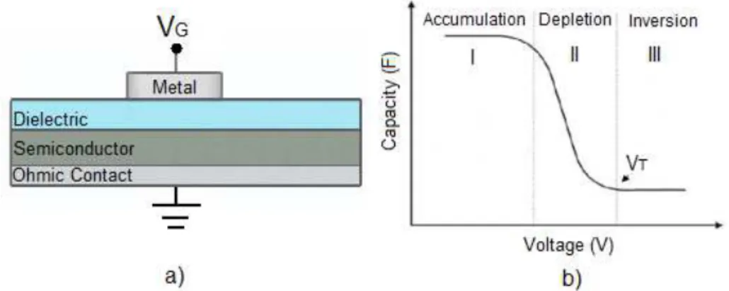
Capacitors are part of electronic circuits used to store electric energy by the accumulation of unbalanced level of electrical charges within and are at the basis for dielectric application, development and performance. There are several types, sizes and shapes of capacitors, but the typical structure consists of two conductors, designed plates, which transport equal but opposites charges (- q and + q) with an insulator between them with a specific thickness (d) [45]. The charge is given by the potential difference (V) between the plates and by the capacitance (C):
q = CV (1.1)
The capacitance of the capacitors, measured in Farads, with parallel plates depends of the plates area (A), the thickness of the dielectric (d) between them, the dielectric constant of the insulating material (k) and vacuum permittivity (ε0). Thus, C depends on the plates itself but is independently on the charge or potential difference [39, 46].
C = kε0Ad (1.2)
In Metal-Insulator-Semiconductor (MIS), the capacitance changes with the applied voltage due to the presence of a semiconductor, such as silicon. To achieve the capacitance value in MIS structures, shown in Figure 1.3 a), the characterisation is done with capacitance-voltage (CV) curves and involves the application of a bias voltage at the capacitor terminals. The voltage applied is then divided to the semiconductor and the insulating oxide, so according to that, the total capacitance (CT) of the MIS structure is equal to the capacities of the oxide (Cox) and the semiconductor depletion layer (CD) associated in series [45, 47–49]:
1 CT =
1 Cox+
1
4
As a result, there are three operation domains in a MIS capacitor, shown in Figure 1.3 b) accordingly to the applied voltage sweep.
Figure 1.3: a) MIS structure and b) Example of a typical CV curve for a p-type semiconductor based MIS.
I) With no voltage applied, the p-type semiconductor has holes, or majority carriers, in the valence band. When the MIS structure is forward biased, which means, a negative voltage (VG) is applied between the top electrode (metal gate) and the semiconductor, more holes will appear in the valence band on the insulator-semiconductor interface. This phenomenon occurs because the metal negative charge causes an equal net positive charge to accumulate at the insulator-semiconductor interface. This operation domain is called accumulation.
For a MIS capacitor with p-type semiconductor, the dielectric capacitance is measured in the accumulation region, because the voltage in this region is negative enough for the capacitance to remain constant, being the semiconductor capacitance infinite and the CV curve almost plane. Moreover, in this region, the CT of the capacitor is given by Cox, since the capacitor behaves as one parallel plate capacitor. II) When a small positive voltage is applied between the electrodes of the capacitor, the major carriers are repelled from the dielectric-semiconductor interface. This state of semiconductor is called depletion because the surface of the semiconductor has no more major carriers. This area of the semiconductor acts as a dielectric because it can no longer contain or conduct charge. The total capacitance measured is now equal to Cox and semiconductor CD in series, resulting in a decrease value of measured capacitance. Since the capacitance in the metal gate increases, the depletion region starts to disappear, which leads to the reduction of the capacitance.
III) The positive voltage in the metal gate, creates electron-holes pair and attracts electrons, or minor carriers, towards the gate. Once again, due to the excellent properties of the insulator, the minor carriers accumulate in the dielectric-substrate interface. This layer of minor carriers is called inversion layer since the carrier polarity is inverted. When VG is higher than the threshold voltage (VT), the depletion region reaches a maximum depth and further gate-voltage increases do not further deplete the semiconductor. When the depletion region reaches maximum depth, CT measured in high frequencies is Cox in series with CD. This capacitance is often referred as the minimum capacitance, and in CV curve reaches a plateau, as seen in Figure 1.3 b) [12, 39, 41, 47, 50].
1.4
Thin Film Transistors (TFTs)
Thin film transistors (TFTs) have in the past decades become one of the most, if not the most, relevant device in microelectronics, mainly used as on-off switches in active matrix backplanes of flat panel displays (FPDs). A TFT is a specific field effect transistor (FET), comprising three electrodes, gate, drain and source, one semiconductor placed between the drain and source, and a dielectric (insulator) placed between the gate electrode and the semiconductor (Figure 1.4) [2, 41].
5
The most common TFTs structures are the staggered and coplanar, depending if the source-drain and gate electrodes are on opposite sides or on the same side of the semiconductor. In each structure, there are two possible configurations, top-gate and bottom gate, depending on whether the gate electrode is on top or bottom of the structure.
Figure 1.4: Structure of a TFT in a staggered bottom-gate configuration.
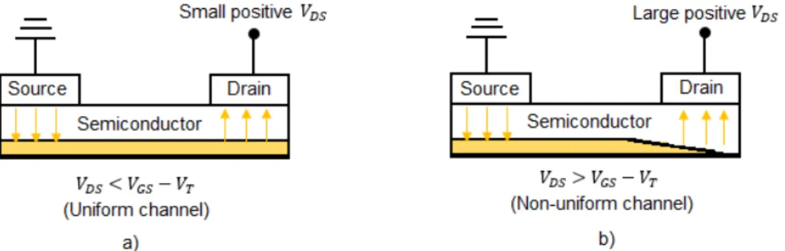
TFTs have two different working domains, depending of the voltage applied between the drain and source (VDS). Assuming an n-type TFT, if the gate voltage is lower than the threshold voltage (VGS <
VT), no matter the value of the VDS applied, the channel modulation will not occur, corresponding to the
TFT off-state. The ideal operation of an n-type TFT depends on the presence of electrons accumulation in the channel between the dielectric and semiconductor, as explained above, which only happens if VGS> VT. For VGS> VT, provided that a positive voltage VDS is applied, current flows between the drain and source electrodes (IDS). For a small but positive VDS, IDS increase linearly to the voltage applied,
corresponding to the linear regime. The TFT is on saturation regime when IDS is constant with the increasing VDS [2, 39, 41, 51].
➢ Linear regime, when VDS< VGS− VT, IDS is described by [2, 51]:
IDS=WL CiµFE[(VGS− VT)VDS−12 VDS2] (1.4)
Where, Ci is the gate capacitance per unit area, µFE is the field effect mobility, W is the channel width and L is the channel length. For very small VDS, the quadratic term can be neglected, yielding a linear
relation between IDS and VDS. In this situation, the accumulated charges are considered to be uniformly
distributed throughout the channel (Figure 1.5 a)) [2, 51].
Figure 1.5: Schematics of different operation regimes of a TFT in on-state a) linear regime b) saturation
regime (pinch-off).
6
IDS=2L CW iµSAT(VGS− VT)2 (1.5)
Where µSAT is the saturation mobility. In this regime, the accumulation layer near the drain region becomes depleted, leading to the saturation of IDS. This phenomenon is referred as pinch-off (Figure 1.5
b)) and starts to occur when VDS= VGS− VT [2, 51].
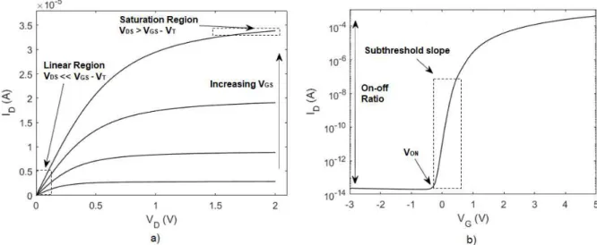
The static characteristics of TFTs are accessed by their output and transfer characteristics, as shown in Figure 1.6 a) and b), respectively.
Figure 1.6: Typical a) output and b) transfer characteristics of a n-type oxide TFT.
In the output characteristics, VDS is swept for different values of VGS, allowing one to see both TFT
regimes described above. The transfer characteristics, where VGS is swept for a constant VDS, allows to
extract numerous number of quantitative electrical parameters, such as on-off ratio, turn-on voltage Von,
mobility (µ) and subthreshold slope (SS), described below [39]:
SS = (|𝜕log (𝐼𝜕𝑉 𝐷)
𝐺𝑆 |) −1
𝑚𝑎𝑥
(1.6)
The mobility of a TFT can be extracted using two different methods, according to the regime:
➢ Field effect mobility (µFE) – obtained from the transconductance (𝑔𝑚), linear regime:
µ𝐹𝐸 =𝑊𝑔𝑚
𝐿 𝐶𝑖𝑉𝐷𝑆 (1.7)
➢ Saturation mobility (µSAT)– obtained from the 𝑔𝑚, saturation regime:
µ𝑆𝐴𝑇 =
(𝜕√𝐼𝜕𝑉𝐷𝑆
𝐺𝑆 ) 2
𝑊 2𝐿 𝐶𝑖
7
2
Materials and Methods
In order to study the influence of polyvinylpyrrolidone (PVP) on the aluminium oxide dielectric produced by solution, different concentrations of organic material for two PVP materials of different molecular weight. To fully understand the properties of the hybrid dielectric in TFTs, two standard semiconductors IGZO and zinc-tin oxide (ZTO) developed by the researchers of CENIMAT were used [52].
2.1
Hybrid AlO
x/PVP Precursor Solutions Preparation and Characterisation
The dielectric precursor solutions were prepared with aluminium nitrate nonahydrate (Al(NO3)3 . 9H2O,
Roth, ≥ 98%), dissolved in 10 mL of 2-methoxyethanol (2-ME, 𝐶3𝐻8𝑂2, ACROS Organics, 99 %), in
a concentration of 0.1 M. For combustion reaction precursor solutions, the fuel urea (CO(N𝐻2)2,
Sigma-Aldrich, 98 %) was added to the precursor solutions after they had been under constant stirring for 10 min. To conclude, the polyvinylpyrrolidone (PVP) was added ((C6H9NO)n, Sigma-Aldrich, molecular
weight of 10000 and 40000, PVP 1 and PVP 2 respectively), to the precursor solutions which were maintained under constant stirring for at least 1 hour. All precursor solutions were stirred at 450 rpm in air environment at room temperature, to a volume of 10 mL and were filtrated through 0.20 µm hydrophilic filters. The solution combustion synthesis of Al2O3 from aluminium nitrate and urea
reaction can be seen in Annex A.
To guarantee the redox stoichiometry of the reaction, for aluminium nitrate based precursors the urea to aluminium nitrate molar proportion was 2:5:1 (Annex A). Different percentages of PVP, 0.2 %, 0.5 %, 0.8 %, 1 %, 5 %, 10 % and 25 %, either for PVP 1 or PVP 2 were added. These percentages are the weight of the polymer in solution volume (10 mL).
Thermal, chemical and physical characterisation of the precursor solutions were performed by thermogravimetry and differential scanning calorimetry (TG-DSC), Fourier Transform Infrared (FTIR) spectroscopy and viscometer. TG-DSC analysis were performed under air atmosphere up to 550 °C with a 10 °C/min heating rate in an aluminium crucible using simultaneous thermal analyser, Netzsch (TG-DSC – STA 449 F3 Jupiter). FTIR data was verified using an Attenuated Total Reflectance (ATR) sampling accessory (Smart iTR) equipped with a single bounce diamond crystal on a Thermo Nicolet 6700 Spectrometer. The spectra were acquired with a 45° incident angle in the range of 4500-525 cm-1 and with a 4 cm-1 resolution. The pH was also studied, and the analysis was obtained using simple colour strips method.
The viscosity tests were performed using a Cap01 spindle at a temperature of 30 °C. The characterisation was done using different rotations per minute (rpm), in order to guarantee an optimal study of the viscosity properties of the precursor solutions and an optimal correlation factor, BROOKFIELD Cap 2000+.
2.2
Thin Film Deposition and Characterisation
Prior to deposition all substrates (p-type silicon wafer and soda-lime glass with an area of 2.5×2.5 cm2) were cleaned in an ultrasonic bath at 60 °C in acetone for 15 min, then in 2- isopropanol for 15 min and dried under nitrogen (N2) prior to a brief cleaning in deionised water; followed by a 15 min UV/Ozone surface activation step for a distance lamp of 7 cm using a PSD-UV Novascan system.
Thin films were deposited by spin coating, a single layer of all the conditions of Al2O3 with PVP1 or
PVP2 precursor solutions with a concentration of 0.1 M for 35 s at 2000 rpm (Laurell Technologies). This was followed by an immediate hot plate annealing at 200 °C for 30 min in ambient conditions, to ensure the exothermic reaction.
8
The films structure was assessed by glancing angle X-ray diffraction (GAXRD) performed by an X’Pert PRO PANalytical powder diffractometer using with Cu Kα line radiation (λ = 1.540598 Å) with angle of incidence of the X-ray beam fixed at 0.75 °.
The surface morphology was investigated by atomic force microscopy (AFM, Asylum MFP3D) and scanning electron microscopy (SEM, Zeiss Auriga Crossbeam electron microscope). Spectroscopic ellipsometry measurements to determine the thickness of thin films deposited on silicon substrates were
made over an energy range of 1.5−5.0 eV with an incident angle of 70 ° using a Jobin Yvon Uvisel
system. The acquired data were modulated using the DELTAPSI software, and the fitting procedure was done pursuing the minimization of the error function (𝜒2).
ATR FTIR spectroscopy characterisation of thin films deposited on Si substrates was performed under the same conditions as described above for precursor solutions. The optical properties were obtained using a Perkin Elmer lambda 950 UV/VIS/NIR spectrophotometer, where the transmittance (T) was obtained from 200 nm to 800 nm for thin films deposited on glass substrates.
2.3
Electronic Devices Fabrication and Characterisation
Metal−insulator-semiconductor (MIS) capacitors were produced by Al2O3/PVP 1 or Al2O3/PVP 2 thin
film deposition onto p-type silicon substrates (1−10 Ω cm). Aluminium gate electrodes (80 nm thick) with an area of 7.85 × 10⁻³ cm2were deposited by resistive thermal evaporation via shadow mask. An 80 nm thick aluminium film was also deposited on the back of the silicon wafer to improve electrical contact. Electrical characterisation was performed measuring both the capacitance−voltage and capacitance-frequency characteristics in the range of 1 kHz to 1 MHz of the devices using a semiconductor characterisation system (KeySight B1500A).
The TFTs were produced in a staggered bottom-gate, top-contact structure by depositing Al2O3/PVP 1
or Al2O3/PVP 2 thin films onto p-type silicon substrates, as described above. The semiconductor film
was sputtered onto the Al2O3/PVP 1 and Al2O3/PVP 2 thin films via shadow mask by radiofrequency
magnetron sputtering without intentional substrate heating in an AJA ATC 1300-F system present in the CEMOP cleaning room. The IGZO deposition, from a ceramic target ((LTS Chemical) Inc.), parameters were a composition target of 1:2:2, an Air:O2 flow ratio of 14:3, a pressure deposition 2.3 mTorr, a power of 100 W, pre-sputtering time of 10 min and a deposition time of 18 min 40 s to obtain a 30 nm thickness. A cross section of produced devices was performed by focused ion beam (FIB). In FIB milling experiments, Ga+ ions were accelerated to 30 kV at 5 pA and the etching depth was around 200 nm. The ZTO semiconductor film deposition was sputtered using AJA ATC 1800 and a target with 1:1 Zn:Sn atomic ratio. The ZTO parameters were: Air:O2 flow ratio of 50:5.36, a pressure deposition 2.3 mTorr, a power of 160 W, a pre-sputtering time of 10 min and a deposition time of 7 min to obtain a 30 nm thickness.
Finally, source and drain aluminium electrodes (80 nm thick) were deposited by resistive thermal evaporation via shadow mask, defining a channel width (W) and length (L). Hereafter the IGZO and ZTO TFTs with the dielectric layers were annealed at 180 °C, for 1 hour in air. An 80 nm thick aluminium film was also deposited on the back of the silicon wafer to improve electrical contact. The current−voltage characteristics of the devices were obtained using a semiconductor parameter analyser (Agilent 4155C) attached to a microprobe station (Cascade M150) inside a Faraday cage, in the dark and room temperature.
9
3
Results and Discussion
In this chapter, the results concerning the precursor solutions characterisation, the thin films characterisation and electric characterisation of MIS capacitors and TFTs will be presented and discussed.
3.1
Hybrid AlO
x/PVP precursor solution characterisation
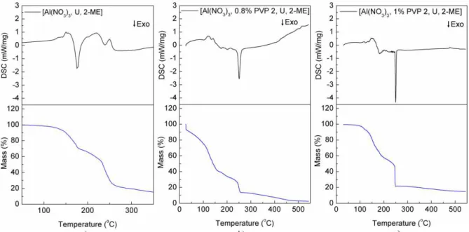
The first step was to perform a thermal analysis to investigate the decomposition behaviour of the metal oxide precursors. Figure 3.1 shows the thermogravimetry (TG) and differential scanning calorimetry (DSC) results for aluminium nitrate Al(NO3)3 precursor solution, as well as the same precursor solution
with 0.8 % and 1 % of PVP 2, using urea (U) as fuel to ensure the combustion reaction and 2-methoxyethanol (2-ME) as solvent.
Figure 3.1: TG-DSC analysis of a) aluminium nitrate precursor solution b) aluminium nitrate precursor with 0.8
% of PVP 40000 and c) aluminium nitrate precursor with 1 % of PVP 40000. All the solutions used U as fuel and 2-ME as solvent.
The aluminium nitrate precursor using urea as fuel and 2-ME as solvent, without the polymer PVP, exhibits an exothermic peak near the 177 °C and a smaller endothermic peak at 250 °C attributed to the degradation of residual organics.
As shown in Figure 3.1, aluminium nitrate precursor with PVP 40000 exhibit an intense exothermic peak at 250 °C, corresponding to the abrupt mass loss that occurs, regardless of the PVP percentage. Given this, PVP in the precursor solution leads to a shift of the exothermic peak towards higher temperatures, meaning that higher temperature might be needed for the combustion reaction to occur and produce the metal oxide. However, the TG-DSC sample preparation requires concentration of precursor solution and is expected that in film form the required temperature is lower. A smaller endothermic peak is obtained at 127 °C, attributed to the solvent evaporation [27].
Thermal analysis of the precursor solutions indicate that the minimum temperature required for full degradation is 250 °C, right after the exothermic peak.
The FTIR spectra of hybrid AlOx/PVP precursor solutions was performed to identify the elements
10
Figure 3.2: FTIR spectra of hybrid precursor solutions made with a) PVP 10000 and b) PVP 40000.
As Figure 3.2 shows, all the hybrid precursor solutions have many organic peaks between 1200 cm-1 and 800 cm-1, associated with 2-ME. This result is important to understand the amount of organics present on the precursor solutions and what needs to be removed, since the organics can influence the good performance of the device. Moreover, both spectra show vibrational modes typical of 2-ME and PVP. Most of the peaks in the spectra are from 2-ME, which is expected since it is the main component of the precursor solution. For higher PVP % their characteristic peaks become more evident, such as at 1680 cm-1. In addition, there is no difference between the spectra of PVP 1 and PVP 2 because it is the same material, only the molar mass is different.
For lower PVP %, is expected that the bands of PVP do not become visible due to the small amount of PVP used.
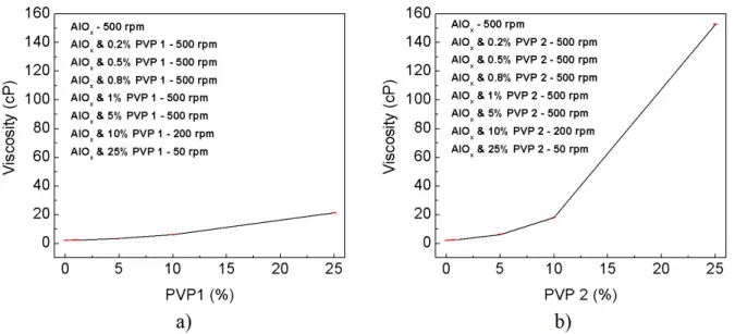
The viscosity analysis of the hybrid precursor solutions was done to study the influence that different concentrations of PVP had when depositing the thin film using spin-coating, associated with the solution dispersion. The viscosity of the solutions measured are visible in Figure 3.3.
Figure 3.3: Viscosity analysis of hybrid precursor solution with a) PVP 10000 and b) PVP 40000.
11
The hybrid precursor solutions with PVP 2, have higher viscosity in comparison with PVP 1 above 1 % of the respective polymer, which is expected since the PVP 2 molecular weight is four times higher than the molecular weight of PVP 1.
The influence of the increase viscosity of the precursor solutions is also visible on the solution dispersion when the spin coating is done, making the thin film much more heterogeneous as noted by optical microscope images in Annex C.
By changing the viscosity properties of the solution, this can be applied in different techniques, like inkjet printing and screen printing, in future work.
The pH analysis of the precursor solutions was performed to study the influence of PVP in aluminium nitrate precursor solution, using a simple strip colorimetric method.
pH measurement of precursor solution show that regardless of the PVP molecular weight, for small PVP concentrations the acidity does not change when compared with the precursor solution with only aluminium nitrate, with a constant value of 2-3, avoiding hydroxides formation. Increasing the PVP concentration slightly increase the pH value.
3.2
Thin Films Characterisation
3.2.1
Optical Characterisation
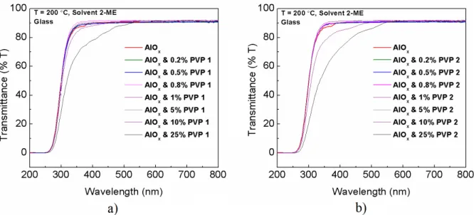
The transmittance analysis of thin films produced with the hybrid precursor solutions was measured on glass between 190-800 nm. By analysing Figure 3.4, it was observed that transmittance is around 91 % for small PVP concentrations and becomes less transparent when the polymer concentrations is higher. This behaviour is clearer in Figure 3.4 b), because as mentioned in section 3.1, the viscosity of the hybrid precursor is higher when using PVP 2, hence the transmittance becomes highly affected for higher PVP concentrations, particularly above 5 %.
Figure 3.4: Transmittance spectra of thin films in a glass substrate a) AlOx with different PVP 1 concentrations
and b) AlOx with different PVP 2 concentrations.
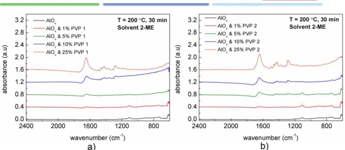
The FTIR spectra of hybrid AlOx/PVP thin films was performed to identify the elements through
characteristic spectra and notice the disappearance of organics peaks, still present on the hybrid precursor solutions seen in section 3.1. The study was performed under the same conditions as the precursor solutions.
12
Figure 3.5: FTIR spectra of various hybrid thin films a) AlOx/PVP 1 b) AlOx/PVP 2.
The main peaks can be seen at 1650 cm-1, 1423 cm-1, 1290 cm-1, 1105 cm-1 and 615 cm-1 and the Table 1 shows the corresponding chemical bond to their respective peak. After correction of the atmosphere contribution, the spectra for all samples are found to be similar, with only slight changes. The most significant change is the increase of the peak at 1650 cm-1 with the increase of PVP %.
Table 1: Characteristic absorbance peaks and associated vibrational modes of the corresponding chemical bonds
for the spectrum of AlOx/PVP thin film on silicon [54, 55].
Position (cm-1) Chemical Bond
1650 C=O, C-N (Stretch)
1423 C-N, CH2 (Sissor)
1290 CH2 (Wag), C-N (Stretch)
1105 Si-O (Transversal Optic Stretching)
615 Al-O2 (Transversal Optic Bending)
3.2.2
Spectroscopic Ellipsometry
The thickness of all dielectric thin films was measured by spectroscopic ellipsometry due to small thickness. Figure 3.6 shows the thickness of all the thin films measured.
Figure 3.6: Thickness of hybrid thin films of a) PVP 10000 and b) PVP 40000 measured with spectroscopic
13
As expected, the thickness of the thin films increases with PVP concentration, regardless of molar mass, but it is also clear that the increasing of thickness is more significant when used PVP 2, as expected from viscosity results seen in section 3.1. The model should be improved in order to achieve more reliable results concerning 𝜒2, particularly to higher than 1 % of PVP in alumina thin films. Another option is to use profilometry in these conditions. In Annex D, the table regarding the thickness of these films are displayed, as well as the mathematic model used to characterise the thin films.
The thickness of two hybrid dielectrics films with 2 layers each was also studied. The results can be seen in Table 2.
Table 2: Thickness (nm) of multilayer hybrid dielectric thin films.
AlOx/PVP with 2 layers
1% PVP 1 92.50 ± 0.35
1% PVP 2 116.28 ± 1.1
The results show that the thickness of these multilayer hybrid dielectrics have twice as much thickness as the monolayer hybrid dielectrics with the same amount of PVP.
3.2.3
Structure and Morphological Characterisation
The structure of the hybrid thin films AlOx/PVP, deposited on silicon substrates, was studied using glancing angle x-ray diffraction. The structure of the dielectric thin film is truly important because amorphous structures do not suffer from grain boundaries, allowing to have low leakage current, a surface much smoother and uniform films, affording better interface properties with the semiconductor layer [2, 40].
The absence of diffraction peaks in the diffractograms, shown in Figure 3.7, confirms the amorphous structure of the deposited hybrid films on Si, independently of the PVP molar mass and concentration. The diffractograms of were performed in smaller ranges since expected diffraction peaks for Al2O3 are within that range [56–59].
Figure 3.7: GAXRD diffractograms of hybrid dielectric thin films produced at 200 °C of a) AlOx/PVP 1 and b)
AlOx/PVP 2.
The phase of AlOx was not performed because it is known from previous research that even at 350 °C it is amorphous [31].
14
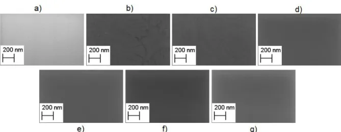
(AFM). The determination of the surface roughness (Rms) was acquired in alternate mode and the topographic images were analysed in data analysis software Gwyddion.
Figure 3.8 shows that the roughness of the dielectric thin films decreases with the increase of PVP concentration until 0.8 %, nevertheless remains below 2.5 nm for 1 % of PVP which reveals an adequate smooth surface.
Figure 3.8: Morphological characterisation of hybrid dielectrics deposited onto Si substrate a) AlOx b) AlOx/0.5
% PVP 1 c) AlOx/0.8 % PVP 1 d) AlOx/1 % PVP1 e) AlOx/0.5 % PVP 2 f) AlOx/0.8 % PVP 2 g) AlOx/1 % PVP
2.
To evaluate the surface of the dielectrics, measurements using scanning electron microscopy (SEM) was performed.
Figure 3.9: Surface characterisation of dielectric films deposited on Si substrate with a 200 µm scale of a) AlOx
b) AlOx/0.2 % PVP 1 c) AlOx/0.2 % PVP 2 d) AlOx/0.5 % PVP 1 e) AlOx/0.5 % PVP 2 f) AlOx/0.8 % PVP 1 g)
AlOx/0.8 % PVP 2.
The images obtained in SEM confirm the amorphous nature of the hybrid dielectrics, as well as a smooth and uniform surface, regardless of the PVP and their percentage.
Another important aspect in the dielectric layer characterization is its elemental composition. This characterization was performed with SEM equipped with energy dispersive X-ray (EDS). This analysis allows the identification of chemical elements that constitute the dielectric, and the main objective was to observe the atomic % difference of carbon in different hybrid dielectrics.
Table 3: Carbon atomic percentage of hybrid dielectrics measured by EDS
PVP Type C Atomic (%)
AlOx/0.2 % PVP
C Atomic (%) AlOx & 0.8 % PVP
PVP 1 15.30 21.98
15
As depicted from Table 3, the increase concentration of PVP in the dielectric increases the carbon on the films. Moreover, the hybrid dielectric with PVP 400000 exhibit more atomic % of carbon in comparison to the dielectric with PVP 10000. Because the PVP 40000 has a larger chain, is harder to remove the carbon residuals and because of that, the residual C % is superior. Although the amount of material used in PVP 10000 and PVP 40000 is the same, the way the atoms are distributed is different because the PVP 40000 has larger chains (molecular weight four times superior), even though the global amount is identical.
The morphology of IGZO TFTs with a hybrid solution based dielectric thin film annealed at 180 °C for 30 min was studied using SEM-FIB. SEM-FIB cross-section images of bottom gate (AlOx/0.8 %PVP 2)/IGZO TFTs produced on highly doped p-Si (gate) with aluminium source/drain contacts are shown in Figure 3.10.
Figure 3.10: SEM-FIB cross section image of bottom gate AlOx with PVP 2/IGZO TFTs produced on highly
p-Si (gate) with aluminium source/drain contacts.
The average thickness of aluminium source/drain electrodes and the hybrid dielectric measured in this mode, showed similar thickness results achieved in ellipsometry for the dielectric and the 80 nm postulated. The IGZO layer is difficult to see because of the small thickness (30 nm) compared to all the other layers.
All the semiconductors were patterned to achieve a channel with W/L = 10 (Annex F) and the concentration of AlOx studied for all the conditions was always 0.1 M.
3.3
Electrical Characterisation of Hybrid solution based AlO
x/PVP capacitors
The performance of TFTs is highly dependent on the characteristics of the insulator and the properties of the interface dielectric-semiconductor. For this, the insulating layer has been studied using metal-insulator-semiconductor (MIS) structures.
The characterisation of these structures is made by different curves, capacitance-voltage (CV), capacitance-frequency (Cf) and current-voltage (IV), which enables to attain information about the devices leakage current, the dielectric constant and the breakdown field of the dielectric layer.
The capacitance is an important parameter to measure since it is important in lowering the operating voltage. A large capacitance is known to accumulate more carriers which allows the device to turn on at a lower voltage. However, large capacitances dielectrics are known to have other issues such as high leakage current and structural imperfections, due to the small thickness of the dielectric layer.
16
The Cf curves enable to see the changes of capacitance with the frequency (in a range of 1 kHz to 1 MHz) to different applied voltages VGS. The IV curves allow to determine the current behavior when it
passes through the device according to VGS.
The frequency chosen to measure capacitance of the dielectrics was 100 kHz to have all the dielectrics under the same conditions, since in certain cases, for lower frequencies the capacitance increases exponentially with the decreasing frequency, which can be explained due to ionic polarisation contribution and consequently may influence the mobility value, making it unreliable.
The dielectric constant of the films characterised were obtained to study the variation of this parameter when organic material is introduced.
3.3.1
Influence of PVP 1 in AlO
xcapacitors
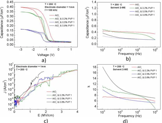
Figure 3.11 exhibits all the measurements done regarding the MIS capacitors when using hybrid dielectrics with PVP 10000.
Figure 3.11: a) Capacitance-voltage (CV) b) capacitance-frequency (Cf), c) current-voltage (IV) and d) dielectric
constant-frequency curves characteristics of p-type Si/(AlOx/PVP 1)/Al MIS capacitors produced with hybrid
solution precursor using urea (U) as fuel in 2-methoxyethanol (2-ME) annealed at 200 °C for 30 min.
The hybrid dielectric with 0.8 % PVP have a lower capacitance when compared to the other dielectrics, Figure 3.11 a), which is expected, since the capacitance decreases with the increase thickness and this dielectric is the thicker compared to the others. The hysteresis appears to decrease with the implementation of PVP 1 due to the local confinement of mobile ions inside the polymer networks and consequent suppression of electron-double-layer (EDL) effects [46, 61].
In Figure 3.11 b), it is possible to see a slight variation of the capacitance with the frequency when comparing the AlOx dielectric with the hybrid dielectrics, moreover towards lower frequencies the capacitance slightly increases due to the presence of mobile ions.
17
d)), and it is visible that to lower frequencies the dielectric has higher k in particularly in the hybrid dielectrics with higher PVP concentration.
Using the equation 1.2, the dielectric constant of the films was obtained.
Table 4: Dielectric constant of AlOx and hybrid films of AlOx/PVP 1.
Temperature Dielectric Thickness (nm) Capacitance (nF/cm2) Constant (k) Dielectric
200 °C
Al2O3 15.21 398 6.84
Al2O3 & 0.2%
PVP1 20.26 349 7.99
Al2O3 & 0.5%
PVP1 32.08 165 5.98
Al2O3 & 0.8%
PVP1 42.95 164 7.96
As depicted from Table 4, the dielectric constant of Al2O3 was lower than expected (~9), but still in agreement with reported values for solution process aluminium oxide [21]. The hybrid dielectrics appear to have higher dielectric constant, except the dielectric with 0.5 % PVP, because of their superior thickness and mobile ions in the polymer network combined with Al2O3 [46].
The MIS capacitors characterisation of hybrid dielectrics with high PVP 1 concentrations were also obtained but achieved low capacitance values because of their high thickness (Annex E). Their dielectric constant was also evaluated.
3.3.2
Influence of PVP 2 in AlO
xcapacitors
Figure 3.12 exhibits all the measurements done regarding the MIS capacitors when using hybrid dielectrics with PVP 40000.
Figure 3.12: a) Capacitance-voltage (CV) b) capacitance-frequency (Cf) and c) current-voltage (IV) curves
characteristics of p-type Si/(AlOx/PVP 2)/Al MIS capacitors produced with hybrid solution precursor using urea
18
Similar to what was seen with the hybrid dielectrics with PVP 1, the dielectrics using PVP 2 exhibit the same characteristics. Figure 3.12 a) shows that the capacitance of the hybrid dielectrics decreases with the increasing PVP concentration, as well as the hysteresis parameter, due to the same reason mentioned for PVP1.
The capacitance only suffers slight variation with the frequency, making these dielectrics stable at a wide range of frequencies when compared with the ones using PVP 1. Considering Figure 3.12 c), the hybrid dielectrics with higher PVP 2 concentrations, possess less leakage current density and the breakdown voltage tends to decrease, due to higher densification in the film.
The dielectric constant of these dielectrics is shown in Table 5. This parameter is higher when the dielectric has PVP 40000 than without, due to the same reason mentioned earlier for PVP 10000. Even though the dielectric constant is an intrinsic property of the materials, by using the equation 1.2, the different thicknesses and consequently capacitances, the higher values of dielectric constant of the insulators when using PVP 40000 can be explained.
Table 5: Dielectric constant of AlOx and hybrid films of AlOx/PVP 2.
Temperature Dielectric Thickness (nm) Capacitance (nF/cm2) Constant (k) Dielectric
200 °C
Al2O3 15.21 398 6.84
Al2O3 & 0.2%
PVP2 21.27 235 5.65
Al2O3 & 0.5%
PVP2 35.33 221 8.82
Al2O3 & 0.8%
PVP2 49.35 123 6.86
The capacitors using hybrid dielectric with high PVP 2 concentrations were also obtained, but the capacitance values measured were extremely low (Annex E). Their dielectric constant was also evaluated.
All dielectrics produced presented a high density of leakage current owing to the presence of fixed charges attributed to structural defects in the dielectric-silicon interface. The effect of trapped charge in the dielectric, typically located at the interfaces of the constituent layers of the capacitor, must also be considered [39].
Considering the results obtained in Figure 3.11 and Figure 3.12, for both PVP 10000 and PVP 40000 respectively, even though the capacitors made with the hybrid dielectric with PVP 1 achieved higher capacitance values, the variation of the capacitance with frequency is lesser in the hybrid dielectrics with PVP 2, especially at higher percentages.
The breakdown voltage was better in the hybrid dielectrics with PVP 1, because of the smaller thickness in comparison with dielectrics produced with PVP 2. Still, before reaching the breakdown voltage and for the same electric field applied, the hybrid dielectrics with PVP 2 presented less leakage current density.
The relation between the k and the frequency was also performed as seen in Figure 3.12 d) and, it is observed the same phenomenon as when using PVP 10000.
3.3.3
Influence of the number of hybrid dielectric layers
19
Figure 3.13: a) Capacitance-voltage (CV) b) capacitance-frequency (Cf) and c) current-voltage (IV) curves
characteristics of p-type Si/ 2layers of AlOx/PVP /Al MIS capacitors produced with hybrid solution precursor
using urea (U) as fuel in 2-methoxyethanol (2-ME) annealed at 200 °C for 30 min.
According to Figure 3.13 a), both hybrid dielectrics exhibit better capacitances than the monolayer hybrid dielectrics, regardless of the PVP. Although the thickness of the hybrid film with PVP 2 is higher, the capacitance is still better, which do not follow the equation 1.2. This can be due to enhanced interface formed with PVP 2. In the capacitance-frequency curves there is a considerable variation of the capacitance with frequency due to the mobility charge carriers according to the hopping conduction mechanism. Suggesting that the dielectric constant of the structure is frequency-dependent relaxation [62].
The leakage current density tends to increase with the number of layers of the hybrid dielectrics. One more layer results in one more interface, where the defects can become more relevant, compromising the relation between higher dielectric thickness less leakage current, being the last one to prevail. Table 6 shows the dielectric constant of these multilayer hybrid dielectrics.
Table 6: Dielectric constant of multilayer hybrid films of AlOx/PVP
Temperature Dielectric (2 layers)
Thickness
(nm) Capacitance (nF/cm2) Constant (k) Dielectric
200°C
Al2O3 & 1% PVP1 92.50 77.35 8.01
Al2O3 & 1% PVP2 116.28 97.40 12.80
20
3.4
TFTs Electrical Characterisation
The hybrid thin films of AlOx/PVPusing different precursor solutions in 2-ME has been implemented in TFTs with different semiconductors, IGZO and ZTO by sputtering, for being standards semiconductors (deposited by sputtering), allowing to focus on the dielectric behaviour on TFTs under different conditions. The hybrid thin films with high PVP percentages (≥ 1 %), either PVP 1 or PVP 2, could not be measured since the channel did not modulate.
3.4.1
IGZO TFTs with AlO
x/PVP 1 hybrid dielectric
Figure 3.14 a) shows a higher Ioff current when PVP is introduced, resulting in a smaller current ratio, but exhibits less gate leakage current. In addition, the output transfer curves of AlOx/TFT and hybrid 0.8 % PVP 1/TFT and the trend of the TFTs electrical parameters are presented in Figure 3.14 b) and c), respectively.
The output characteristics revealed that the TFTexhibited a clear pinch-off and excellent saturation as shown by the flatness of the IDS curves for high VDS, except the last VGS, due to the resistance contact, concerning the hybrid TFT. Given this, both output curves obtained demonstrate that the entire thickness of the IGZO channel was completely depleted of free electrons. The saturation IDS of the TFTs containing only AlOx was higher than that of the AlOx/PVP device, explained by the resistance of the channel layer and better electrical properties of the inorganic materials. All the TFTs with hybrid dielectric made presented similar output curves. The Table 7 depicts the values shown in Figure 3.14 c). The higher On/Off ratio was achieved by the AlOx dielectric, moreover, the ratio tends to decrease with more PVP because of the gate dielectric and the carrier concentration of the IGZO channel layer [8]. Still, it was expected the current ratio to decrease because of the organic material.
Figure 3.14: a) transfer curves, b) output curves and c) electrical parameters variation of IGZO/TFTs with hybrid
dielectrics of PVP 10000.
Subthreshold slope swing (SS) is an important device performance parameter for high-speed and low-power operation, in other words, is related to the dielectric-semiconductor interface quality, by interface trap states. The increase value of this parameter, means higher defects densities for dielectrics with more organics (PVP). The higher value of trapping states is reflected on the TFT, since it decreases the mobility of the carriers, explaining the decrease of mobility and On/Off ratio [8, 63].
21
The threshold suffers a negative VT shift. This instability behaviour is caused by the mobile ions present in the dielectric. A significant amount of positively charged mobile ions move towards the dielectric-semiconductor interface. Although these positive mobile ions contribute for the accumulation of electrons in IGZO channel layer, due to the slow response characteristics of mobile ions, they tend to remain near the dielectric-semiconductor interface causing a negative shift of transfer curves [64–66].
Table 7: Characteristic parameters of IGZO/AlOx/PVP 1 TFTs for different concentrations of dielectric annealed
at 200 °C.
Dielectric SS (V/dec)
VON
(V) Ion/Ioff
Hysteresis (V)
VT (V)
µsat (cm2/V∙s)
AlOx
0.092 ± 0.004
0.072 ± 0.003
(1.40 ± 0.15) ×105
0.073 ± 0.007 0.297 ± 0.026 23.81 ± 0.24
AlOx & 0.2% PVP1
0.203 ± 0.017
0.372 ± 0.105
(8.83 ± 1.29) ×103
0.076 ± 0.010 0.302 ± 0.092 14.78 ± 1.82
AlOx & 0.5% PVP1
0.202 ± 0.032
0.233 ± 0.147
(5.14 ± 0.52
×103
0.099 ± 0.041 0.168 ± 0.104 17.20 ± 1.88
AlOx & 0.8% PVP1
0.290 ± 0.049
0.501 ± 0.090
(2.07 ± 1.13) ×103
0.154 ± 0.058 0.374 ± 0.110 11.51 ± 1.19
3.4.2
IGZO TFTs with AlO
x/PVP 2 hybrid dielectric
From Figure 3.15 the On/Off ratio of the TFTs decrease with PVP 2, according to the transfer curves, still, for more PVP is exhibited less gate leakage current, except for 0.5 % PVP. The Von shifts towards zero for higher PVP 2 percentages, as shown Figure 3.15 c). The output curve with PVP 2 showed equal characteristics in comparison with the TFTs with PVP 1.
Figure 3.15: a) transfer curves, b) output curves and c) electrical parameters variation of IGZO/TFTs with hybrid
22
The output curves show that the inorganic TFT have higher output impedance in the saturation region, and the flatness of the curves are more evident.
The transfer curves shown in Figure 3.15 a) displayed worst On/Off ratio for hybrid dielectrics than for the inorganic TFT, which is natural because organics have worst electrical properties. In addition, there is a slight decrease of the gate leakage current when PVP is introduced.
SS increases with PVP 2, due to higher defects densities in the dielectrics. Nevertheless, the SS parameter is smaller when using PVP 2 then PVP 1, meaning lesser interface trap states at the dielectric-semiconductor, which is related to a more compacted and dense film, enhancing the interface properties. As the TFTs with PVP 1, the VT also suffered a negative shift due the same reasons already mentioned in section 3.4.1. It is achieved minimal hysteresis due to the local confinement of mobile ions inside the polymer networks [46].
The superior mobility can be described by the aforementioned polymer network confinement of the mobile ions in the hybrid gate dielectric. Moreover, the formation of electric double layer (EDL) at the dielectric-semiconductor interface, enhances the electrical properties of the TFTs. The formation of EDL is due to the mobile ions, including -OH that resides in the gate dielectric, allowing a substantial number of electrons to be accumulated near the dielectric-semiconductor interface [46]. In addition, the thickness in these hybrid dielectrics is higher leading to lesser capacitance values, resulting in higher mobilities, as described in equation 1.8 shown in section 1.4.
For lower frequencies the capacitance increases exponentially because of the response time to changes in the electric field applied or due to the ionic polarisation contribution. For those reasons the dielectric capacitance might be underestimated and consequently the mobility can also become overestimated. Moreover, the electronic mobility of IGZO depends on the number of hydroxyl group content in the dielectric film, thus the mobility is higher with PVP 40000 since there are more OH groups [63]. To help the comprehension of Figure 3.15 c), Table 8 is portrayed below.
Table 8: Characteristic parameters of IGZO/AlOx/PVP 2 TFTs for different concentrations of PVP annealed at
200 °C.
Dielectric
SS (V/dec)
VON
(V) Ion/Ioff
Hysteresis (V)
VT (V)
µsat (cm2/V∙s)
AlOx
0.092 ± 0.003
-0.072 ± 0.004
(1.40 ± 0.12) ×105
0.073 ± 0.007 0.297 ± 0.026 23.81 ± 0.24
AlOx & 0.2% PVP2
0.143 ± 0.007
-0.358 ± 0.002
(1.15 ± 0.07) ×104
0.051 ± 0.008 -0.363 ± 0.019 30.90 ± 1.90
AlOx & 0.5% PVP2
0.152 ± 0.009
-0.315 ± 0.035
(1.09 ± 0.20) ×104
0.036 ± 0.008 -0.270 ± 0.033 20.03 ± 2.69
AlOx & 0.8% PVP2
0.169 ± 0.012
0.078 ± 0.004
(4.75 ± 1.44) ×103
0.026 ± 0.003 0.123 ± 0.061 40.24 ± 1.13
23
Regarding the TFTs with hybrid dielectrics, the TFTs that achieved enhanced properties were the ones made with PVP 40000. These TFTs had better interface properties between the dielectric and semiconductor, reflected in smaller values of SS. In addition, both On/Off ratios and mobilities obtained had enhanced results. The mobilities achieved in the TFTs with PVP 40000 were even higher than the TFT with AlOx. Moreover, the turn-on voltage of the TFTs was closer to zero and the leakage current was lower. Therefore, polymer with higher molecular weight offers enhanced electrical properties, mainly because it can better fill the pores formed by using solution-base processes.
A comparison between the mobilities obtained in this work and recent research regarding TFTs using hybrid dielectrics can be seen in Annex G.
3.4.3
Influence of the semiconductor layer
Figure 3.16 shows the transfer and output curves of the hybrid ZTO/TFTs, followed by Figure 3.17 that presents all the TFTs parameter variation. According the figures mentioned, is possible to understand that the quality of the interface between the hybrid dielectric and ZTO is worse in comparison with the IGZO.
Figure 3.16: Transfer curves of ZTO/(AlOx/PVP 1)/TFTs and its output transfer, a) and b) respectively and transfer
curves of ZTO/(AlOx/PVP 2)/TFTs and its output transfer, c) and d) respectively.
The output curves are optimal, since there is a clear pinch-off and excellent saturation as shown by the flatness of the curves. The device containing PVP 40000 exhibited larger output impedance in the saturation region than the device containing PVP 10000.
![Figure 1.2: Relationship between the band gap and the dielectric constant for different materials considered to be high-k dielectrics [39]](https://thumb-eu.123doks.com/thumbv2/123dok_br/16698382.743915/25.892.279.625.91.378/figure-relationship-dielectric-constant-different-materials-considered-dielectrics.webp)