Glass Microfluidic platforms for molecular
detection by SERS
Dissertação para Obtenção do Grau de Mestre em Engenharia Micro e Nanotecnologias
Orientador: Prof. Doutor Hugo Manuel Brito Águas, Faculdade de Ciências e Tecnologia da Universidade Nova de Lisboa
Co-orientadores: Doutora Ana Cláudia Madeira Botas Gomes Pimen-tel, Faculdade de Ciências e Tecnologia da Universi-dade Nova de Lisboa
Prof. Doutor José Ricardo Franco Tavares, Facul-dade de Ciências e Tecnologia da UniversiFacul-dade Nova de Lisboa
Júri
Presidente: Prof. Doutor Rodrigo Martins Arguente: Doutor César Laia
i
Glass Microfluidic platforms for molecular detection by SERS
Copyright © [Bernardo Matos Alves Costa Ferreira], Faculdade de Ciências e Tecnolo-gia, Universidade Nova de Lisboa.
iii
Two roads diverged in a yellow wood, And sorry I could not travel both And be one traveller, long I stood And looked down one as far as I could To where it bent in the undergrowth;
Then took the other, as just as fair, And having perhaps the better claim, Because it was grassy and wanted wear; Though as for that the passing there Had worn them really about the same,
And both that morning equally lay In leaves no step had trodden black. Oh, I kept the first for another day! Yet knowing how way leads on to way, I doubted if I should ever come back.
I shall be telling this with a sigh Somewhere ages and ages hence: Two roads diverged in a wood, and I—
I took the one less traveled by, And that has made all the difference.
v
Acknowledgements
No final desta longa e importante etapa na minha vida, queria agradecer a todos que de uma forma ou outra me acompanharam, me ajudaram e tornaram este momento pos-sível. Deste modo quero começar por agradecer à Faculdade de Ciências e Tecnologias da Universidade de Lisboa, e ao departamento de Ciências dos Materias por me terem acolhido tão bem durante estes anos neste grande curso de Micro e Nanotecnologias. Por isso, agradeço também, ao Prof. Dr. Rodrigo Martins e à Prof. Dra, Elvira Fortunato por terem criado este curso e dado todas as ferramentas necessárias e não só, para a formação de engenheiros com espirito crítico, prática laboratorial e bases que poucos ou nenhum outro curso têm. Queria também agradecer ao departamento de conservação e restauro por disponibilizarem o Raman.
De seguida gostaria de agradecer ao meu orientador Hugo Águas por me ter acei-tado neste projecto e acompanhado durante todo o processo com a partilha de conheci-mentos, ideias e sempre disponível. À minha coorientadora Dra. Ana Pimentel, por me ter ajudado na síntese de nanorods e partilhado ideias que me ajudaram em várias situa-ções. Ao meu coorientador Professor Ricardo Franco pelos conselhos, ajuda e encoraja-mento ao longo do projecto. À Mestre Andreia Araújo por todo o tempo disponibilizado, pelas várias deposições na câmara limpa, e todas as ideias, conhecimentos e orientações ao longo do projeto. À Mestre Maria João, por toda a paciência, ajuda no Raman, enco-rajamento, constante disponibilidade, por me guiar e apoiar em todo este percurso. À Daniela Gomes pelas magníficas imagens SEM, sem elas a tese não seria a mesma coisa. À Alexandra Gonçalves e à Sónia Pereira pela paciência, ajuda, disponibilidade e boa disposição. À Ana Carolina pela ajuda no laser. Ao Pedro Alves pela ajuda no PDMS. A todos os colegas, amigos que me acompanharam neste percurso. Obrigado Paul, Jaime, Rodrigo, Anas, Andreia, Rosa, Tomás, Iris, Bruno, Emanuel, Gonçalo, Almeida, Gabi.
A todos os meus amigos, que me têm acompanhado sempre, desde sempre. Tocha e Vítor, especialmente, por todos estes anos a aturar-me, um Obrigado. Aos meus grandes amigos Flores, um irmão para mim, Nandes, César e Braga, tamos cá! Sem vocês não seria a mesma coisa.
Glass Microfluidic platforms for molecular detection by SERS
vi
motivação. Aos meus avós por todo o seu apoio, carinho, força e todos os bons momentos. To Jana, thank you for all the patience, all this moments.
Há sem dúvida quem ame o infinito, Há sem dúvida quem deseje o impos-sível,
Há sem dúvida quem não queira nada -
Três tipos de idealistas, e eu nenhum deles:
Porque eu amo infinitamente o finito, Porque eu desejo impossivelmente o possível,
Porque eu quero tudo, ou um pouco mais, se puder ser,
Ou até se não puder ser...
vii
Resumo
Atualmente têm sido desenvolvidas tecnologias para a deteção de contaminantes alimen-tares face à crescente preocupação na saúde pública. Todavia, os métodos hoje existentes são morosos, dispendiosos e complexos para serem aplicados na indústria alimentar. As-sim, o presente trabalho tem como objetivo o desenvolvimento de um dispositivo de mi-crofluídica viável para o uso da espectroscopia de Raman aumentada pela superfície (SERS).
A SERS consiste numa técnica simples, robusta, sensível e rápida para a deteção de componentes vestigiais, podem ser vantajosamente aplicada à deteção de contaminantes alimentares. Foi realizado um estudo dos vários parâmetros de síntese hidrotermal assis-tido por microondas para crescimento de nanorods de óxido de zinco (temperatura, o tempo e pH). Posteriormente, os nanorods de óxido de zinco foram revestidos por nano-partículas de prata (espessuras de 2, 4, 6 e 8 nm), formadas por deposição física de vapor (PVD) de prata, originando o substrato SERS, AgNP@ZnONR. A eficiência dos vários substratos produzidos foi semelhante independentemente da espessura de prata aplicada, observando-se valores de enhancement factor (EF) de SERS entre ~105- ~106.
Paralela-mente foram desenvolvidos nanorods em forma de obeliscos tendo resultado numa boa eficiência em SERS, apresentando EF~106.
Finalmente, foi criado um dispositivo de microfluídica em PDMS o qual permitiu conduzir uma solução de rodamina-6G sendo observado o seu sinal de SERS no interior do dispositivo. Os ensaios desenvolvidos no decorrer da presente dissertação permitiram inferir sobre o comportamento do sinal de SERS em relação aos parâmetros geométricos dos componentes do substrato para SERS.
ix
Abstract
Nowadays due to increasing concerns in public health, technologies have been developed for the sensitive detection of food contaminants. Since current methods are time-consum-ing, expensive and complex to operate, this project has as the objective to develop a mi-crofluidics device for surface enhanced Raman spectroscopy (SERS).
SERS consists in a simple, robust, sensitive and fast technique for detection of ves-tigial components that can be advantageously adapted to the detection of food contami-nants. In order to develop an appropriate substrate for SERS, a study was performed of different parameters for the hydrothermal synthesis of zinc oxide nanorods (temperature, time and pH). Afterwards, they were covered with silver nanoparticles with different thicknesses (2, 4, 6 e 8 nm) deposited by physical vapour deposition (PVD), originating the substrate Ag NPs@ZnONRs. The efficiency of the different substrates was similar, regardless the thickness of silver, with enhancement factor (EF) values around 105~106.
Simultaneously, obelisk nanorods were developed with good SERS efficiency, and EFs around 106.
Finally, it was created a microfluidics device in PDMS, which allowed to observe the SERS signal of a rhodamine-6G solution in its interior. The assays performed in the work allowed to infer the behaviour of SERS signal with different geometric parameters of components of SERS substrates.
xi
Contents
Acknowledgements ... v
Resumo ... vii
Abstract ... ix
Contents ... xi
Index of Tables ... xiii
Index of figures ... xv
1 Introduction ... 1
1.1 Surface-Enhanced Raman Spectroscopy ... 1
1.2 General concepts of SERS... 3
1.3 ZnO structures ... 4
1.4 Microfluidics device ... 5
2 Materials and Methods ... 7
2.1 Deposition of the ZnO seed layer ... 7
2.2 Synthesis of ZnO Nanostructures ... 7
2.3 Deposition of Ag nanoparticles ... 8
2.4 SERS Analyte ... 8
2.5 Fabrication of the Microfluidics chip ... 9
2.6 Characterization techniques... 10
3 Results and discussion ... 13
3.1 Morphological characterization ... 13
3.2 Characterization of Ag nanoparticles ... 21
3.3 Raman and SERS signal of Rhodamine 6G ... 23
3.4 SERS assays for ZnO NRs with Ag NP ... 25
3.5 SERS efficiency with Obelisk Nanorods ... 29
3.6 Fabrication of PDMS microfluidics device ... 32
4 Conclusion and Future Perspectives ... 35
References... 37
5 Attachments ... 41
Attachment A ... 41
Attachment B ... 43
Attachment C ... 45
Attachment D ... 47
Glass Microfluidic platforms for molecular detection by SERS
xiii
Index of Tables
Chapter 3 – Results and discussion
Table 3. 1 - Vibrational bands assignments for R6G. ... 25 Table 3. 2 – Dimensions of obelisk nanorods. ... 31 Table 3. 3 - Dimensions of Microfluidics device. ... 33
Chapter 5 – Attachments
Table 5. 1 - Laser parameters for Microfluidics device pattern ... 41 Table 5. 2 - Diameter and length variation of ZnO NRs at different temperatures and
xv
Index of figures
Chapter 1 - Introduction
Figure 1.1 - Energy diagram representing (from left to right) the elastic Rayleigh scattering and the inelastic Stokes (left) and Stokes (right) Raman scattering (adapted from4,6). ... 1
Figure 1.2 – A) Schematic representation of Raman analysis (right side) and SERS with metal NPs (left side); B) Illustration of LSPR effect; C) Electromagnetic
enhancement for dimer configurations of two spheres. ... 2 CHAPTER 2–MATERIALS AND METHODS
Figure 2. 1 - Schematic of production of ZnO NRs with Ag NPs: a) glass substrate; b) sputtering of ZnO seed layer on the glass substrate; c) growth of ZnO nanorods by hydrothermal method assisted by microwave radiation; d) e-beam silver film and formation of Ag NPs. ... 8 Figure 2. 2 - Schematic of SERS platform analysis with R6G: a) SERS platform of ZnO
NRs with Ag NPs; b) Drop of 2 µL of R6G onto SERS platform; c) SERS signal measurement with excitation laser 633 nm. ... 9 Figure 2. 3 - Schematic of the production of microfluidic device: (A) PDMS substrate;
(B) Etching of the PDMS by CO2 laser, making the microfluidics channel and
well; (C) UVO treatment of PDMS substrate and glass substrate with SERS platform; d) Sealing of SERS platform with PDMS by applying pressure; (E) Microfluidics device. ... 10
CHAPTER 3RESULTS AND DISCUSSION
Figure 3.1 - SEM images taken from the top of ZnO NRs produced by hydrothermal growth at the indicated times and temperatures. ... 14 Figure 3. 2 - Changes in density with: a) number of NRs per µm2 with different
synthesis temperature; b) number of NRs per µm2 with different synthesis time; c)
area occupied by NRs with synthesis temperature; d) area occupied by NRs with synthesis time. ... 15 Figure 3. 3 - Variation of ZnO NRs length and diameter with synthesis temperature. .. 15 Figure 3. 4 - Variation of NRs length and diameter with synthesis time ... 16 Figure 3. 5 – SEM images of ZnO NRs synthesized with different pH values: a) 7; b) 9; c) 11; d) 12. ... 17 Figure 3. 6 - Representative XRD pattern of ZnO NRs; indexed peaks corresponding to
Glass Microfluidic platforms for molecular detection by SERS
xvi
Figure 3. 7 - Variation of ZnO grain size with seed layer thickness. ... 19 Figure 3. 8 - SEM image of ZnO NRs grown with different seed layers thickness: a) 100
nm; b) 150 nm; c) 200 nm; d) 300 nm (left side); SEM images of cross section of ZnO NRs with different seed layer thicknesses. a) 100 nm; b) 150 nm, c) 200 nm; d) 300 nm (right side). ... 19 Figure 3. 9 – Variation of ZnO NRs length and diameter with seed layer thickness. (The lines are only for visual aid). ... 20 Figure 3. 10 - Growth rate of ZnO NRs with different seed layer thicknesses. (The lines are only for visual aid). ... 21 Figure 3. 11 - SEM image of ZnO NRs with different Ag NPs thickness of 2, 4, 6 and 8
nm. ... 22 Figure 3. 12 - a) Absorptance spectra of SERS substrates with uncoated ZnO NRs and
ZnO NRs with 2 nm, 4 nm, 6 nm and 8 nm mass thickness of silver. b) Ag NPs diameter with Ag NPs film thickness. ... 23 Figure 3. 13 - UV-Vis absorption spectrum of R6G with its molecular structure inset. 23 Figure 3. 14 - Raman and SERS spectrum of R6G. (a) Raman spectrum of 10-3 M R6G
aqueous solution (x10 magnified) and (b) SERS spectrum of 103 M R6G aqueous
solution on glass substrate with Ag NPs@ZnO NRs under 633 nm laser excitation. ... 24 Figure 3. 15 - Average EF calculated using the vibrational bands areas at 1509 cm-1 for:
a) 2 nm Ag NPs; b) 4 nm Ag NPs; c) 6 nm Ag NPs; d) 8 nm Ag NPs. ... 26 Figure 3. 16 - Average EF values with Nanorods length. ... 27 Figure 3. 17 - Schematic image of the fabrication of an arrays of ZnO NRs decorated
with Ag NPs on glass substrate (adapted from52). ... 27
Figure 3. 18 - SERS spectrum of R6G using different inclination. ... 29 Figure 3. 19 - XRD pattern of ZnO obelisk NRs; indexed peak corresponding to the
typical wurzite hexagonal structure. ... 30 Figure 3. 20 – SEM images of obelisk nanorods with: a) Ag film. High and low
magnification; b) Ag NPs deposited by PVD. ... 31 Figure 3. 21 – Comparison of the average EF values of obelisk Ag film with obelisk
NPs and Standard hexagonal NRs with NPs. ... 32 Figure 3. 22 - PDMS microfluidics device image (left) and its schematic with R6G
(right). ... 33 Figure 3. 23 - SERS spectrum of R6G in PDMS device. (a) Background spectrum of
device without R6G; b) SERS spectrum of 10-4 M R6G in PDMS device under 633
xvii CHAPTER 5–ATTACHMENTS
Figure 5. 1 - XRD of ZnO seed layer thickness: a) 100 nm; b) 150 nm; c) 200 nm; d) 300 nm. ... 45 Figure 5. 2 - Average EF values calculated using the vibrational bands areas at 1360 and
1509 cm-1 for: a) 2 nm Ag NPs; b) 4 nm Ag NPs; c) 6 nm Ag NPs; d) 8 nm Ag NPs. ... 47 Figure 5. 3 - Average EF values of different Ag thickness with NRs length: a) 173 nm;
xix
Abbreviations
Absp Absorptance
AgNP Silver nanoparticle
CE Chemical enhancement
CO2 Carbon dioxide
EF Enhancement Factor
EM Electromagnetic enhancement
FWHM Full width at half maximum
GC Gas chromatography
HeNe Helium-neon laser
HPLC High-performance liquid chromatography LAFED Laser assisted flow deposition
LSPR Localized surface plasmon resonance
NP Nanoparticle
NRs Nanorods
PDMS Polydimethylsiloxane
PVD Physical vapour deposition
Rtot Total reflectance
R6G Rhodamine 6G
SEM Scanning electron microscopy
SEM-FIB Scanning electron microscopy-Focused ion beam SERS Surface-enhanced Raman spectroscopy
UV-Vis Ultraviolet-Visible
UVO Ultraviolet-Ozone
Ttot Total transmitance
XRD X-Ray Diffraction
Glass Microfluidic platforms for molecular detection by SERS
xxi
Symbols
Au Gold
Ag Silver
C Carbon
CRAMAN Raman concentration
CSERS SERS concentration
CH2 Methylene
IRAMAN Raman intensity
ISERS SERS intensity
M Molar
Min Minute
nm Nanometers
µL Microliter
xxiii
Motivation and objectives
Nowadays despite extensive methods to protect public health, disease outbreaks from harmful chemicals and microbial threats still occur. Although the continuous ad-vances in chemical analysis such as gas chromatography (GC)1 and high-performance
liquid chromatography (HPLC)2 led to significant improvements in automation,
measure-ment time, sensitivity and accuracy, they still suffer certain disadvantages, such as the need of trained personnel, complex and time-consuming sample preparation.
As an alternative, a promising technique is the surface-enhanced Raman spectros-copy (SERS). SERS allows to screen single or multiple contaminant classes simultane-ously, is simple, fast, inexpensive and a reliable method.3
Zinc oxide was chosen as the platform for the SERS structures for its electrical properties, low price and excellent performance in supporting SERS substrates. ZnO pro-vides the possibility to create nanostructures, which, when coupled with Ag, can generate higher detection sensitivity and thus stronger signal enhancements.
Microwave-assisted synthesis has fast reaction time (compared to conventional method such has furnace), less thermal losses and allows the control of kinetic conditions (time, temperature and pressure), making it a very interesting and promising technique for the development of zinc nanostructures.
Thermal evaporation assisted by electron beam was used to obtain silver nanopar-ticles (AgNP). This process promotes a good homogeneity and stability, by forming self-assembled NPs.
For its precise control and ability to create a lab-on-a-chip, microfluidics devices offer great advantages for SERS platforms towards point of need applications.
Glass Microfluidic platforms for molecular detection by SERS
xxiv
1
1
Introduction
1.1
Surface-Enhanced Raman Spectroscopy
In early 20th century two vibrational spectroscopy methods appeared infrared (IR)
and Raman via two different mechanisms: the direct absorption of photons (IR) and the inelastic scattering of photons (Raman). These molecular vibrations were unique for every given molecular structure. Raman spectroscopy has been less used than IR due to its relative weak signals, fluorescence interference and high cost of equipment. As an advantage in relation to IR spectroscopy, especially for biological systems, Raman has less interference from water signals.4,5
Raman spectroscopy relies on the inelastic scattering of a photon from a molecule where the frequency changes precisely matching the difference in vibrational energy lev-els (Figure 1.1).5
Glass Microfluidic platforms for molecular detection by SERS
2
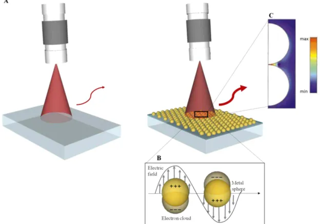
In 1974 it was found that weak Raman scattering signals can be greatly enhanced using noble metal nanostructures (Figure 1.2).6,7
Figure 1.2 – A) Schematic representation of Raman analysis (right side) and SERS with metal NPs (left
side); B) Illustration of LSPR effect; C) Electromagnetic enhancement for dimer configurations of two spheres.
1.1.1
Electromagnetic enhancement effect
The electromagnetic enhancement (EM) is due to the interaction of an electromag-netic wave with a metal surface. The electromagelectromag-netic wave, with a specific angular fre-quency, excites resonantly the delocalized conduction electrons in a metal (plasmons), resulting in an amplification of the electromagnetic fields near the surface.4,8,9
When the valence electrons of the metal nanoparticle are in a collective oscillation with the frequency of the incident light, occurs the LSPR (Figure 1.2).4,10
1.1.2
Chemical enhancement
3
(1.1)
the metal, resulting in a change of the Raman scattering cross-section of the molecule. This changes lead to enhancements in the range of one to three order of magnitude for Raman scattering, significantly smaller than EM.4,11
1.2
General concepts of SERS
The most common SERS active substrates are gold (Au) and silver (Ag) colloids with diameters between 10 and 200 nm. The utilization of colloidal nanoparticle solution presents an advantage as a SERS substrate because it minimizes the burning of samples due to heat dissipation through water, allowing the use of high laser power to enhance the Raman signal. Moreover, the presence of large numbers of nanoparticles allows the ac-quisition of a stable average-spectrum. However, one drawback associated with liquid colloidal nanosubstrates is the required nanoparticle aggregation, where an uncontrolled exaggerated nanoparticles clump may happen, leading to a loss of LSPR.3,12
Comparing Ag and Au, Ag presents a higher enhancement due to being more plas-monically active in visible and near IR regions, but Ag is air sensitive while gold is more chemically stable and able to be conjugated with biomolecules.9,13,14
SERS enhancement depends highly on the substrates designs, LSPR can be modu-lated using a variety or parameters as shape, dimension, interparticle gap and environ-mental surroundings. Thus, the possibilities for manufacturing SERS active surfaces in-novative techniques are vast, as nanolithography15, self-assembly techniques16 and
chem-ical synthesis of colloidal metal nanoparticles17.
1.2.1
SERS enhancement factor and
hot spots
SERS enhancement factor (EF) quantifies the overall Raman signal enhancement by comparing the average SERS signal for the adsorbed molecule on a metal surface, normalized with the normal Raman signal of the same molecule in solution. The average SERS EF can be calculated using the following equation18:
𝐸𝐹 =𝐼𝐼𝑆𝐸𝑅𝑆
𝑅𝐴𝑀𝐴𝑁×
𝐶𝑅𝐴𝑀𝐴𝑁
𝐶𝑆𝐸𝑅𝑆
Where ISERS and IRAMAN are the intensities of a particular vibrational band in an
analyte spectrum (in this project: 1360 and 1509 cm-1 for R6G), for SERS and normal
Raman spectra respectively; while CRAMAN is the concentration that produces Raman
Glass Microfluidic platforms for molecular detection by SERS
4
metallic nanostructure.12 In some literature this formula can be reported as analytical
en-hancement factor (AEF).
Raman signal enhancements as high as 1014 can occur in hot spots on SERS
sub-strate due to the combined electromagnetic (EM), chemical enhancement (CE) and reso-nance signal enhancement mechanisms.9,13 The hot spots are localized between adjacent
nanoparticles (< 10 nm) (near-field regions), (Figure 1.2 C) responsible for the global SERS effect. Hence, SERS is a highly distance-dependant phenomenon and the shape and structure of the nanostructures affect significantly the enhancement. A very close gap between the nanoparticles is therefore beneficial for the creation of extremely strong lo-calized electric fields enhancements.19,20
1.3
ZnO structures
Zinc oxide (ZnO) nanostructures have been the subject of intensive studies due to their remarkable chemical and physical properties. ZnO is a n-type semiconductor with a wide and direct band gap of 3.3 eV. ZnO physical and chemical properties depend on size, shape, morphology, and crystallinity of the synthesized nanostructures.21–23
Several chemical, electrochemical and physical techniques have been used to grow ZnO nanostructures with different morphologies, as such electrodeposition23,24,
electro-spinning25,26, laser assisted flow deposition (LAFED)27 and hydrothermal synthesis28,
whether by conventional heating or by microwave radiation.23,29
1.3.1
Microwave-assisted synthesis
This technique provides the opportunity to complete reactions, by using different power, in shorter times (minutes), since microwaves are able to transfer directly the energy to the reactive species (molecular heating), promoting reactions and transformations that are difficult and require a longer time in conventional heating.23,29
5
1.4
Microfluidics device
Microfluidics is becoming highly attractive in bioanalysis for its precise control and ma-nipulation of biological samples. Its small size allows the creation of portable lab-on-a-chip devices that facilitate the low detection limits required in biological target identifi-cation. Small devices result in faster reaction times, better temperature control, low en-ergy consumption, parallelisation and portability.30
Although SERS is a highly specific and sensitive analytical technique it is challeng-ing to obtain repeatable and reproducible results under complex experimental conditions. Those problems can be overcomed using a microfluidic channel, for a more regular ge-ometry and minimizing the damage to the biological analytes, the recording time and the sample volumes.31
Microfluidic devices are commonly made from polydimethylsiloxane (PDMS) and other polymers. They can be manufactured by moulding techniques, such as photolithog-raphy and soft lithogphotolithog-raphy which are cheap and suitable for the mass scale production. PDMS is biocompatible, thermally stable up to 150 ºC, has the ability to replicate features with approximately 1 nm resolution and excellent optical properties. PDMS can be sealed reversibly onto substrates by conformal contact due to its elasticity by plasma or UVO treatment. For this reasons PDMS was the chosen material for the present work.7
7
(2.1) (2.2) (2.3)
2
Materials and Methods
In this section, an experimental description is made of the synthesis of the ZnO nanorods and the subsequent deposition of AgNPs techniques by PVD. The substrates fabricated were then tested for SERS efficiency.
2.1
Deposition of the ZnO seed layer
The first step for the fabrication of the Ag NP@ZnO NRs is the deposition of a single layer of ZnO seed on a glass substrate by sputtering at room temperature. A ceramic oxide target with a purity of 99 % has been used for the deposition with the following condi-tions: power density P = 8.2 Wcm-2, distance between the target and substrate, d = 15 cm,
deposition pressure, pd = 4 × 10⁻³ mbar. Prior to the depositions, the chamber was
evac-uated, using a turbo-molecular pump, to 10-6 mbar. For each seed layer thickness it was
used different deposition times: 1 h for 100 nm; 1 h 30 min for 150 nm; 2 h for 200 nm and 3 h for 300 nm.
2.2
Synthesis of ZnO Nanostructures
The ZnO NRs have been synthesized with an aqueous solution of 25 mM zinc nitrate hexahydrate (Zn(NO3)2·6H2O; 98 %, CAS:10196-18-6) and 25 mM
hexamethylenetet-ramine (C6H12N4)2; 99 %, CAS: 100-97-9), both from Sigma Aldrich. Different
parame-ters were tested: synthesis time (5 min, 15 min, 30 min, 45 min), temperature (70 ºC, 100 ºC, 130 ºC, 150 ºC) and pH (7, 9, 11 and 12).32
The aqueous solutions of zinc nitrate and hexamethylenetetramine produce the following chemical reactions33:
(𝐶6𝐻12𝑁4) + 6𝐻2𝑂 → 6𝐻𝐶𝐻𝑂 + 4𝑁𝐻3
𝑁𝐻3+ 𝐻2𝑂 → 𝑁𝐻4++ 𝑂𝐻−
2𝑂𝐻−+ 𝑍𝑛2+→ 𝑍𝑛𝑂(𝑠) + 𝐻 2𝑂
The ZnO obelisk NRs were grown in an aqueous solution of 0.1 M of zinc nitrate hexahydrate (Zn(NO3)2·6H2O; 98%, CAS:10196-18-6) and 0.02 M ammonium chloride
Glass Microfluidic platforms for molecular detection by SERS
8
of the solution was adjust to 10.5 using ammonia.34 The obelisk nanorods were
synthe-sised at 100 ºC for 15 min.
For the growth of ZnO nanostructures, a seeded substrate (20 x 20 mm) was placed face down in the vessel. The synthesis were carried out in a microwave Discover SP, from CEM, with a microwave power of 40 W. After each process, the materials were cleaned with isopropyl alcohol and deionized water.
2.3
Deposition of Ag nanoparticles
The nanoparticles were formed using electron gun-assisted evaporation technique ( Fig-ure 2. 1). The temperatFig-ure was kept at 150 ºC during the thermal evaporation of Ag mass-equivalent layer thickness (2, 4, 6 and 8 nm), with a deposition pressure of 10-5 mbar at a
deposition rate of 0.07 nm·s-1. The thickness and growth rates were inferred by a
cali-brated quartz crystal detector.
Figure 2. 1 - Schematic of production of ZnO NRs with Ag NPs: a) glass substrate; b) sputtering of ZnO
seed layer on the glass substrate; c) growth of ZnO nanorods by hydrothermal method assisted by micro-wave radiation; d) e-beam silver film and formation of Ag NPs.
2.4
SERS Analyte
Tetraethylrhodamine hydrochloride (Rhodamine 6G – R6G) was purchased from Sigma Aldrich without further purification. Due to its high Raman cross section, this compound is commonly used as an analyte to evaluate SERS activity in the substrates. Concentra-tions of R6G solution were from 10-3 M for the control and 10-6 M for all samples. The
9
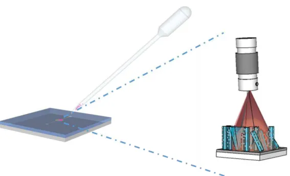
Figure 2. 2 - Schematic of SERS platform analysis with R6G: a) SERS platform of ZnO NRs with Ag NPs;
b) Drop of 2 µL of R6G onto SERS platform; c) SERS signal measurement with excitation laser 633 nm.
2.5
Fabrication of the Microfluidics chip
The PDMS was prepared by mixing the base and the curing agent in a 10:1 ratio of weight. The mixture was stirred and degassed in a vacuum desiccator for 1h. Afterwards, the PDMS was poured into a Petri dish, and degassed again to remove the bubbles and ther-mally cured on a levelled hot plate at 80 ºC. Following, the microfluidics layout was etched by a CO2 Laser (10.6 µm), VLS universal system 3.5 with the time and potency
variation presented in attachment A.
Glass Microfluidic platforms for molecular detection by SERS
10
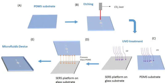
Figure 2. 3 - Schematic of the production of microfluidic device: (A) PDMS substrate; (B) Etching of the PDMS by CO2 laser, making the microfluidics channel and well; (C) UVO treatment of PDMS substrate
and glass substrate with SERS platform; d) Sealing of SERS platform with PDMS by applying pressure; (E) Microfluidics device.
2.6
Characterization techniques
Morphological characterization. The morphology of the NRs was examined by SEM-FIB using a Carl Zeiss AURIGA Crossbeam workstation instrument equipped with an Oxford X-ray Energy Dispersive Spectrometer. The dimensions of the ZnO nanorods were determined from SEM micrographs of 20 individual nanorods, using ImageJ soft-ware.
The crystallinity of the as-prepared materials was determined using a PANalytical
X’Pert PRO MRD X-ray diffractometer, with a monochromatic Cukα radiation source
(wavelength 1.540 598 Å). XRD measurements have been carried out from 10º to 60º (2θ), with a scanning step size of 0.016º.
Optical characterization. The UV-Vis spectroscopy was used to characterize the Ag NPs after their synthesis. The reflectance and transmittance spectra was obtained with UV-VIS-NIR spectrometer (Perkin Elmer lambda 950 UV/VIS/NIR) equipped with an inte-grating sphere, in the wavelength range of 300 – 1100 nm.
11
13
3
Results and discussion
In this chapter the results from the developed work are presented and discussed. This project had the main objective of study the production of SERS substrates using ZnO NRs coated with Ag NPs aiming to maximise their SERS efficiency, and to apply them in a microfluidics chip, to test its viability. Hence, different synthesis parameters of ZnO NRs were tested, followed by morphological, structural and optical characterization through SEM, DRX and UV-Vis spectroscopy respectively and finally Raman spectroscopy was used to analyse SERS efficiency.
3.1
Morphological characterization
In order to study the ZnO NRs produced by hydrothermal growth assisted by microwave radiation, different parameters were tested, such as synthesis temperature, time, pH and ZnO seed layer thickness. The morphology and the ZnO NRs distribution was observed by SEM images.
3.1.1
Effect of temperature and time on the ZnO NRs Synthesis
In Figure 3.1 it is showed the SEM image of the ZnO NRs growth using different synthe-sis times (5, 15, 30 and 45 min) and synthesynthe-sis temperatures (70, 100, 130 and 150 ºC).
Glass Microfluidic platforms for molecular detection by SERS
14
Figure 3.1 - SEM images taken from the top of ZnO NRs produced by hydrothermal growth at the indi-cated times and temperatures.
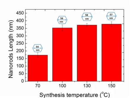
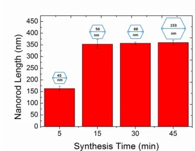
It was observed that by increasing the synthesis temperature from 70 ºC to 100 ºC there was a significant growth of the length of ZnO NRs, around 200 nm. For higher temperatures (130 and 150 ºC), the ZnO NRs did not show a dramatic increase of the growth, leading to a stagnation phase after reaction, possibly because the reagents reached a maximum point and the growth of the NRs stalls, Figure 3. 3. The diameter remained slightly the same. As the synthesis time and temperature increased, the density of nano-rods per area decreased (Figure 3. 2 a, b). Simultaneously, as the time and temperature of the NRs synthesis are increased, the occupied area of NRs per µm2 also increase.
More-over, higher synthesis temperature and time, the longer and wider are the ZnO nanorods, leading to a higher occupation of the glass substrate, with a smaller density.
15
Figure 3. 2 - Changes in density with: a) number of NRs per µm2 with different synthesis temperature; b)
number of NRs per µm2 with different synthesis time; c) area occupied by NRs with synthesis temperature;
d) area occupied by NRs with synthesis time.
Figure 3. 3 - Variation of ZnO NRs length and diameter with synthesis temperature.
Glass Microfluidic platforms for molecular detection by SERS
16
significant increase of diameter is due to Ostwald ripening effect, where the tiny crystal-lites nucleate first followed by the growth of the larger particles due to the energy differ-ence between large and smaller particles.36,37 However their length did not change
signif-icantly after 15 min.
Figure 3. 4 - Variation of NRs length and diameter with synthesis time
Hence the ZnO NRs showed a preferential growth toward vertically and after sta-bilizing the NRs expand horizontally, has it has been described in the literature.22,38–42
3.1.2
Effect of pH on the ZnO NRs synthesis
In the literature is referred that the increasing the pH of the synthesis solution, to grow ZnO NRs by hydrothermal method in the oven, will lead to flower-like nanostruc-tures.21,43,44 Thereby, a study of the influence of pH on ZnO NRs using hydrothermal
17
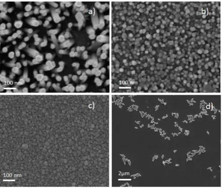
Figure 3. 5 – SEM images of ZnO NRs synthesized with different pH values: a) 7; b) 9; c) 11; d) 12.
With the rise of the pH value of the synthesis solution, using ammonia, the ZnO NRs morphology changed considerably. At a pH value of 9, Figure 3. 5 b), the NRs were significantly smaller (compared to pH 7, Figure 3. 5 a); at pH 11 (Figure 3. 5 c) there was no growth of structure, and at pH 12 (Figure 3. 5 d) there are the appearance of small structures dispersed in the substrate was observed. The results are in accordance to what is described in the literature.43 For the formation of NRs it is influenced by a competition
between crystal growth and etching, therefore, neutral or acidic conditions are required for its formation. According to the literature, by increasing the pH, the morphology of the NRs changes from rods (pH value of 7) to flower-like (around pH 12),43 however, the
fully grown flower like nanostructures were never obtained.
3.1.3
Effect of ZnO Seed layer thickness on the ZnO NRs synthesis and
structural analysis
Glass Microfluidic platforms for molecular detection by SERS
18
(3.1)
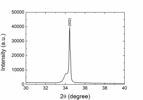
Figure 3. 6 - Representative XRD pattern of ZnO NRs; indexed peaks corresponding to the typical wurzite hexagonal structure.
Figure 3. 6 shows a representative spectrum of all samples with different ZnO NRs obtained by the different synthesis. The sample shows one peak at 34.45 degrees corre-sponding to hexagonal wurzite ZnO crystalline structure, with lattice constants of a=0.3296 nm and c=0.52065. At 34.11 degrees, there is a small protuberance due to the effect of the seed layer (attachment C). All the samples shown have (002) as the preferred orientation, which is in good agreement with literature values.21 The observed high
inten-sity and narrow spectral width of the XRD pattern prove that the ZnO NRs are highly crystalline and with no impurities detected.22It was observed that as the seed layer
thick-ness increased, the intensity of the signal also increased due to its higher crystallinity, has already reported by literature (attachment C).21,22,40
The grain size D, of the ZnO seed layers was calculated by XRD using Scherre’s equation:
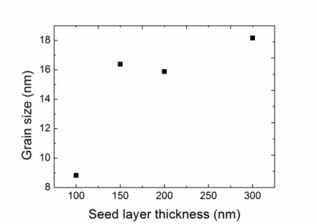
𝐷 = 0.94 × 𝜆 × 𝛽 × 𝑐𝑜𝑠𝜃
where λ is the wavelength of the X-ray radiation, β is the full width at half maximum
(FWHM) and θ the Bragg’s angle. In Figure 3. 7, it is showed the calculated grain size
19
Figure 3. 7 - Variation of ZnO grain size with seed layer thickness.
As expected from the literature, by increasing the seed layer thickness, the grain size also increases.40 Also crystallinity of the ZnO seed layer is improved (attachment C),
making the NRs more aligned, as it can be observed in Figure 3. 8.45–47
The diameter and length of the NRs with different seed layer thicknesses was meas-ured by ImageJ surface imaging and cross-section respectively, Figure 3. 8.
Figure 3. 8 - SEM image of ZnO NRs grown with different seed layers thickness: a) 100 nm; b) 150 nm; c) 200 nm; d) 300 nm (left side); SEM images of cross section of ZnO NRs with different seed layer
thicknesses. a) 100 nm; b) 150 nm, c) 200 nm; d) 300 nm (right side).
Glass Microfluidic platforms for molecular detection by SERS
20
Figure 3. 9 – Variation of ZnO NRs length and diameter with seed layer thickness. (Guide lines for visual aid).
When measuring the dimensions of the NRs, it was expected an increase of the diameter as the seed layer thickness increased, due to the larger grain size. The length of the ZnO NRs, in this case, also increases with the seed layer thickness, which contradicts the results reported in the literature for hydrothermal growth by conventional heating, where NRs length decreases with the seed layer thickness. There were no reports regard-ing the effect of the seed layer on the length of ZnO NRs growth by microwave assisted synthesis.
Also, as the seed layer thickness decreases, there is an increase of density of the NRs, seen Figure 3. 2. As the grain size increases, there are less nucleation points, leading to a smaller density of NRs.32,40,45
21
Figure 3. 10 - Growth rate of ZnO NRs with different seed layer thicknesses. (Trend line for visual aid).
3.2
Characterization of Ag nanoparticles
After ZnO NRs morphology studies, the samples with different morphologies were sub-mitted to PVD for Ag NPs deposition. This last experimental step originated the SERS platforms. The samples were chosen for its higher available area for Ag NPs coupling, leading to more NPs per NRs.
The samples chosen for the following work were Ag NPs with different diameters: 2, 4, 6 and 8 nm onto NRs synthetized with different temperatures (70, 100, 130 and 150 ºC), with synthesis time of 15 minutes. For the study of the ZnO seed layer thickness (100, 150, 200 and 300 nm) and the obelisk nanorods, only the Ag NPs with 6 nm were deposited.
Glass Microfluidic platforms for molecular detection by SERS
22
(3.2) Figure 3. 11 - SEM image of ZnO NRs with different Ag NPs thickness of 2, 4, 6 and 8 nm.
The SEM image of Figure 3. 11 revealed a highly dense and uniform distribution of Ag NPs without large-scaled agglomerates for the NP with 2 and 4 nm thickness. The nanoparticles with 6 and 8 nm thickness, on the other hand, shown the formation of ag-glomerates.
After PVD, the LSPR spectral position and the wavelength range of the SERS sub-strates was determined. Absorptance spectra (Figure 3. 12) were determined from the total reflectance (Rtot) spectra and total transmittance (Ttot) and was calculated using the
following equation:
𝐴𝑏𝑠𝑝 = 100 − 𝑅𝑡𝑜𝑡− 𝑇𝑡𝑜𝑡
There are two characteristic bands present in the absorptance spectra of the SERS substrates: the quadrupole resonances and the dipole resonances. The shorter wavelength peaks correspond to the quadrupole resonances (around 350 nm), whereas the broader peaks, at longer wavelengths, correspond to the dipolar resonances of the Ag NPs. The dipole resonance is due to the collective oscillation of the electrons. This oscillation is determined by four factors: the density of electrons, the effective electron mass, and the shape and size of the charge distribution.8,48,49 Hence, the increase of the Ag mass
23
Figure 3. 12 - a) Absorptance spectra of SERS substrates with uncoated ZnO NRs and ZnO NRs with 2 nm, 4 nm, 6 nm and 8 nm mass thickness of silver. b) Ag NPs diameter with Ag NPs film thickness.
Theoretically to obtain high enhancements require that the incident radiation and the Stokes Raman shifted radiation are in resonance with the metal nanostructure.9
Figure 3. 13 - UV-Vis absorption spectrum of R6G with its molecular structure inset.
3.3
Raman and SERS signal of Rhodamine 6G
Glass Microfluidic platforms for molecular detection by SERS
24
it can generate high fluorescence yield which would prevent the observation of the Raman spectrum.35,51Therefore, the excitation laser wavelength used in this project was 633 nm.
The spectra presented in Figure 3. 14 corresponds to the Raman spectrum of a 10-3
M R6G aqueous solution drop in a glass slide and the SERS spectrum of 10-6 M R6G
aqueous solution on a ZnO NRs with Ag NPs SERS substrate using the 633 nm wave-length excitation laser.
Figure 3. 14 - Raman and SERS spectrum of R6G. (a) Raman spectrum of 10-3 M R6G aqueous solution
(x10 magnified) and (b) SERS spectrum of 103 M R6G aqueous solution on glass substrate with Ag
NPs@ZnO NRs under 633 nm laser excitation.
In both Raman and SERS spectra, the two main vibrational bands correspond to the aromatic C-C stretching modes at 1361 and 1509 cm-1. The assigments of the vibrational
25 Table 3. 1 - Vibrational bands assignments for R6G.
Experimentally observed
bands (cm-1)
Assignment
Raman SERS
1030
1127 in plane C-H bending
1310 1310 In plane xanthene ring breathing, N-H bending, CH2 waggling
1362 1361 Xanthene ring stretching, in plane C-H bending
1509 1509 Aromatic C-C stretching, xanthene ring stretching, C-N stretching, C-H bending, N-H bending
1574 Xanthene ring stretching, in plane N-H bending
1597 1597
1649 1649 Xanthene ring stretching, in plane C-H bending
As can be observed the vibrational bands of the two spectra are coincident, however the SERS signal is more intense and presents a lower noise, despite using a three orders of magnitude lower concentration of R6G. This image clearly illustrates the effect ob-tained by a good SERS substrate on the Raman spectrum of an analyte.
3.4
SERS assays for ZnO NRs with Ag NP
To compare the intensity of the signal from SERS substrates to normal Raman EF values are usually used. In this project, the SERS assays were performed by testing different Ag NPs size with the different ZnO NRs obtained, using drops of 2 µL of R6G solution.
The areas of the vibrational bands at 1360 cm-1 and 1509 cm-1 from R6G SERS
spectra were used to calculate the average EF values. Using a concentration of 10-6 M the
following histograms (with the four different Ag thicknesses) with their average EF val-ues and respective standard-deviations (SD) were calculated for the 1509 cm-1 vibrational
band (the complete histograms with 1360 cm-1 and 1509 cm-1 are presented in the
Glass Microfluidic platforms for molecular detection by SERS
26
It was expected for the average EF values to increase with the longer ZnO NRs due to an increase of Ag NPs density per area and therefore a higher number of Ag NPs would contribute to the SERS signal.
As it can be seen in Figure 3. 15, the expected behaviour did not occur (only EF for the vibrational band of 1509 cm-1 are represented). Using the same NPs size, with
ent NRs length, hence more Ag NPs per area of NRs, there was not a significant differ-ence of the average EF values or a clear correlation between NR length and NP size. All average EF values for the different samples were localized between 105 and 106. A
pos-sible explanation for these results can be attributed to the vertical orientation of the ma-jority of the NRs, hindering the SERS signal from the Ag NPs located at the bottom of the NRs. For the 2 nm mass thickness of Ag (Figure 3.15 a) there is a tendency for the increase of EF with the NRs length, this is attributed to the lower size of the Ag NPs that allow more signal from the bottom of the NRs to contribute to the global EF value. The same can be observed for the 4 nm mass thickness of Ag (Figure 3.15 b) up to 378 nm of NRs length. For larger NPs the effect is lost, and no correlations are found.
Figure 3. 15 - Average EF calculated using the vibrational bands areas at 1509 cm-1 for: a) 2 nm Ag
27
Additionally it was studied the average EF values with the different seed layers thickness, using Ag NPs with 6 nm thickness. Results are presented in Figure 3. 16.
Figure 3. 16 - Average EF values with Nanorods length.
As it was expected from the results obtained previously, the average EF values re-mained approximately the same for the different nanorods length.
For a better understanding of these results, Figure 3. 17 elucidates the fabrication process of the SERS nanostructures.
Figure 3. 17 - Schematic image of the fabrication of an arrays of ZnO NRs decorated with Ag NPs on glass substrate (adapted from52).
Glass Microfluidic platforms for molecular detection by SERS
28
aligned with the nanoparticles attached throughout their surface. Possibly, the values of the average EF for different NRs was not affected by the length of the nanorods because of the polarization of the excitation laser, as it is known that near field distribution (hot spots) have a strong dependence on polarization.53 Since NRs are well aligned, the laser
could only reach the superficial NPs coupled in the NRs. Therefore, only the hot spots localized in the surface were activated, resulting in the same average EF value for the different samples tested.
In terms of Ag thickness variation, for the same NR, it was expected that a higher thickness would result in a creation of clusters, and eventually, the formation of films, which would lead to a loss of the LSPR and consequently a decrease of the EM. However, although the Ag NPs showed an increase of aggregation, they did not change drastically the efficiency of SERS (Figure 3. 11 and attachment E).
Due to the number of available NPs in the NRs for enhancing the SERS signal, not being considerably different, even though the longer NRs have more nanoparticles per nanorod, the NPs in the same NR create hot spots parallel to the laser and, therefore, they do not increase the average EF values. Hence, the thickness of the NP does not impact significantly the average EF value, particularly for the longer NRs and NPs above 4 nm Ag mass film thickness as explained above.
29
Figure 3. 18 - SERS spectrum of R6G using different inclination.
In Figure 3. 18, it is possible to confirm that with a different inclination the signal intensity increases considerably. The respective EF value obtained was around 106,
which, although, was not significantly higher, it was highest EF value attained in the present work.
3.5
SERS efficiency with Obelisk Nanorods
In order to determine the influence of the NRs top morphology a different study was performed using NRs with obelisk form (Figure 3. 20). In this case, to obtain the obelisk tips, it was used a different solution, where hexamethylenetetramine was replaced with ammonium chloride.33 The obelisk NRs were grown at a temperature of 100ºC for 15
min.
Glass Microfluidic platforms for molecular detection by SERS
30
Figure 3. 19 - XRD pattern of ZnO obelisk NRs; indexed peak corresponding to the typical wurzite hexag-onal structure.
By magnifying the spectra it is possible to observe a single peak at 34.25 degrees, corresponding to the crystallographic plans of the hexagonal wurtzite ZnO structure.54 As
in the previous samples, the obelisk NRs also showed a small protuberance at 34.10 de-grees, due to the seed layer. The sample showed (002) as the preferred orientation, which is in good agreement with literature values21. The high intensity of the peak indicates that
the NRs are well aligned and perpendicular to the substrate, as it was observed in SEM images. The high intensity and narrow spectral width show that the nanorods are highly crystalline and with no impurities detected.22
31
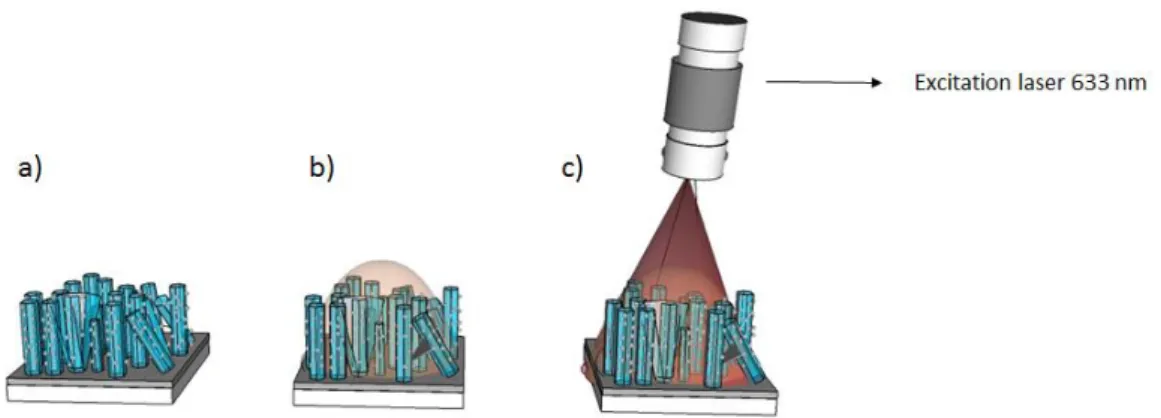
Figure 3. 20 – SEM images of obelisk nanorods with: a) Ag film. High and low magnification; b) Ag NPs deposited by PVD.
In this case, the length obtained when compared with the average length of the previous studied NRs (360 nm) is expressively higher, and the NRs showed a very high density. The density of obelisk nanorods was higher compared to the standard hexagonal NRs, 311 NRs per µm2, as the occupation of NRs per µm2 was around 95%.
Table 3. 2, shows the dimensions of the obelisk nanorods.
Table 3. 2 – Dimensions of obelisk nanorods.
Length (nm) Diameter (nm)
Obelisk NR 1500 171.9
The Ag NPs obtained in the obelisk ZnO NRs were uniform and had an average diameter of 63 nm.
Glass Microfluidic platforms for molecular detection by SERS
32
Figure 3. 21 – Comparison of the average EF values of obelisk Ag film with obelisk NPs and Standard hexagonal NRs with NPs.
The average EF values obtained between the obelisk film NR and the obelisk NP nanorods is approximately the same, around 106. This results are in agreement with those
obtained in the standard hexagonal nanorods with NPs. In the case of the obelisk NRs with Ag thin film, the hot spots are localized only at the sharp protuberances of the rods, and in the obelisk NRs with Ag NPs, the hot spots occur in the inter-gaps of nano-particles in different nanorods. The fact that the average value of EF for film and NP obelisk nanorods suggest that the number of active hot spots created in both is approxi-mately the same. Therefore, like in the hexagonal nanorods, the hot spots are localized mainly in the superficial area of the ZnO Ag structure. Additionally, the enhancement created by the NPs on their own was similar to the enhancement created in the tips of the obelisk NRs.
3.6
Fabrication of PDMS microfluidics device
Knowing the inherent advantages of PDMS microfluidics devices (e.g. high precise con-trol and portability), a device was assembled. Since the used SERS platforms have silver nanoparticles, the microfluidic device also minimise the oxidation of Ag and, conse-quently, degradation of the SERS platform.
First, using a CO2 laser, the channels and well of the microfluidic devices were
33
and 0.05 s/cm respectively), Figure 3. 22. Second, using a UVO treatment (for 30 minutes), the PDMS was bonded to the glass substrate with the NRs previously grew at 100 ºC for 15min.
Figure 3. 22 - PDMS microfluidics device image (left) and its schematic with R6G (right).
The R6G was injected in the channel with a syringe and, with vacuum, pulled to the well. Table 3. 3 presents the diameter of the well and the channels, measured by con-focal microscope.
Table 3. 3 - Dimensions of Microfluidics device.
Well diameter (nm) Channel diameter (nm) Channel depth (nm) Microfluidics device
1x10⁶ 341 161
First it was measured the background signal of the PDMS without R6G and after the SERS spectra of R6G with a concentration of 10-4 M, Figure 3. 23. It was chosen a
concentration of 10-4 M, instead of 10-6 M, for a better perception of the injected R6G in
the microfluidics channel (R6G at 10-4 M has a strong pink colour, which allows a visual
control of the injection of the analyte in the channel).
Since the PDMS was etched using a laser technique, the walls of the channels and well presented a certain roughness. To decrease the formation of this roughness, instead of using laser, using photolithography technique could be a suitable solution for a smoother surface.
Glass Microfluidic platforms for molecular detection by SERS
34
Figure 3. 23 - SERS spectrum of R6G in PDMS device. (a) Background spectrum of device without R6G; b) SERS spectrum of 10-4 M R6G in PDMS device under 633 nm laser excitation.
This spectra is in good agreement with the literature35, where R6G can be easily
identified.
35
4
Conclusion and Future Perspectives
The main objective of this project was to develop efficient nanostructures for SERS ap-plications. For that, different parameters of hydrothermal growth synthesis of ZnO NRs were tested (temperature, time and pH), as well as different seed layer thicknesses (100, 150, 200 and 300 nm) with different Ag nanoparticles thickness (2, 4, 6 and 8 nm) depos-ited by PVD technique.
By increasing the synthesis temperature and time, there is a significant increase in the nanorods length and after an increase of the NRs width, due to the preferential growth ratio of the ZnO NRs. With longer synthesis times, the nanorods obtained have a wider diameter, indicating that after growing vertically, they expand horizontally.
When increasing the pH of the synthesis solution, flower petal like ZnO nanostructures were obtained (pH~12), while NRs formation stopped for pH higher than 7. The formation of ZnO NRs is determined by the competition between crystal growth and etching (caused by acidic conditions).
In the study of the influence of the seed layer thickness, it was possible to conclude that thicker seed layers led to higher crystallinity and larger grain size of the ZnO film. The length and diameter of the NRs increased significantly due to the larger grain size and Ostwald ripening effect. The increase of length with seed layer thickness is possibly due to the larger grain size and crystallinity, leading to a more stable and fast growth, although, it has not been reported yet in the literature.
The use of different ZnO NRs length had the intention of increasing the sensitive area for SERS, allowing the deposition of more nanoparticles, therefore, resulting in a formation of more hot spots and consequentially, an increased enhancement. However, there was no considerable change of enhancement with different nanorods length, using the same NP thickness. Possibly, since the NRs are vertically aligned and the excitation laser is perpendicular to the substrate, only the hot spots closer to the surface are activated, while the ones located in the lower NP are not. Here, the created hot spots are localized between the Ag NP of parallel NRs, while the gaps inter nanoparticles, of the same nano-rod are not activated. This phenomenon has already been reported in literature, where the polarization of the excitation laser is stated to have a variance of four order of magnitude in the EF value.12,20,53 In this present work, instead of changing the polarization of the
Glass Microfluidic platforms for molecular detection by SERS
36
an increase of the SERS signal. Thus, the homogeneity of the average EF values with different NRs length, is indicative of this behaviour. Still, the ZnO NRs showed to be a highly performing reproducible platform for SERS devices.
The study of Ag NPs thickness was tested with the purpose of determine the most efficient in SERS. Although the thicker NPs had a small formation of aggregates, it did not have a direct impact on the average EF value. Since the formation of aggregates would lead for a change of the LSPR, resulting in a change in the EF value. Still, all Ag NPs thicknesses presented good average EF values, around 106 for a concentration of 10-6 M.
The ZnO obelisk nanorods presented a high density, around 95 % of area occupied by NRs. The average enhancement factor values for the obelisk nanorods with thin Ag film were considerable, around 106, similar to the obelisk nanorods with Ag NPs and the
standard hexagonal NRs.
For a more precise control, manipulation and portability it was developed a PDMS microfluidics device. The device showed a good SERS efficiency, and the R6G was de-tected through the PDMS.
In conclusion, all SERS platforms obtained had good SERS efficiency. The overall enhancement factor values for every SERS platform were around 106, using a
concentra-tion of 10-6 M of R6G. It was successfully developed a promising microfluidics device,
using the optimized ZnO NRs, where it was possible detected the analyte (R6G).
37
References
1. Fasano, E., Cirillo, T., Esposito, F. & Lacorte, S. Migration of monomers and plasticizers from packed foods and heated microwave foods using QuEChERS sample preparation and gas chromatography/mass spectrometry. LWT - Food Sci. Technol. 64, 1015–1021 (2015).
2. Hickert, S., Bergmann, M., Ersen, S., Cramer, B. & Humpf, H. U. Survey of Alternaria toxin contamination in food from the German market, using a rapid HPLC-MS/MS approach. Mycotoxin Res. 32, 7–18 (2016).
3. Zheng, J. & He, L. Surface-Enhanced Raman Spectroscopy for the Chemical Analysis of Food. Compr. Rev. Food Sci. Food Saf. 13, 317–328 (2014).
4. Schlücker, S. Surface-Enhanced Raman Spectroscopy : Concepts and Chemical Applications Angewandte. 4756–4795 (2014). doi:10.1002/anie.201205748 5. Siebert, F. & Hildebrandt, P. Theory of Infrared Absorption and Raman
Spectroscopy. Vibrational Spectroscopy in Life Science (Wiley-VCH Verlag GmbG & Co. KGaA, 2008). doi:10.1002/9783527621347.ch2
6. Kleinman, S. L. et al. Structure Enhancement Factor Relationships in Single Gold Nanoantennas by Surface-Enhanced Raman Excitation Spectroscopy. J. Am. Chem. Soc. 135, 301–308 (2013).
7. Wang, C. & Yu, C. Analytical characterization using surface-enhanced Raman scattering (SERS) and microfluidic sampling. Nanotechnology 26, 92001 (2015). 8. Araújo, A. et al. Highly efficient nanoplasmonic SERS on cardboard packaging
substrates. Nanotechnology 25, 415202 (2014).
9. Schlücker, S. Surface-enhanced raman spectroscopy: Concepts and chemical applications. Angew. Chemie - Int. Ed. 53, 4756–4795 (2014).
10. Le Ru, E. C. & Etchegoin, P. G. Rigorous justification of the |E|4 enhancement factor in Surface Enhanced Raman Spectroscopy. Chem. Phys. Lett. 423, 63–66 (2006).
11. Valley, N., Greeneltch, N., Duyne, R. P. Van & Schatz, G. C. A Look at the Origin and Magnitude of the Chemical Contribution to the Enhancement Mechanism of Surface-Enhanced Raman Spectroscopy (SERS): Theory and Experiment. Phys. Chem. (2013). doi:10.1021/jz4012383
12. LeRu, E. C., Meyer, M., Etchegoin, P. G., Le Ru, E. C. & Blackie, E. Surface Enhanced Raman Scattering Enhancement Factors: A Comprehensive Study. J. Phys. Chem. C 111, 13794–13803 (2007).
13. Sakano, T. et al. Surface enhanced Raman scattering properties using Au-coated ZnO nanorods grown by two-step, off-axis pulsed laser deposition. J. Phys. D. Appl. Phys. 41, 235304 (2008).
Glass Microfluidic platforms for molecular detection by SERS
38
Raman Spectroscopy. Annu. Rev. Anal. Chem. 1, 601–626 (2008).
15. Coluccio, M. L. et al. Silver-based surface enhanced Raman scattering (SERS) substrate fabrication using nanolithography and site selective electroless deposition. Microelectron. Eng. 86, 1085–1088 (2009).
16. Khlebtsov, B. N., Khanadeev, V. A., Yu, M., Bagratashvili, V. N. & Khlebtsov, N. G. SERS Substrates Based on Self-Assembled PEGylated Gold and Gold – Silver Core – Shell Nanorods. (2013). doi:10.1021/jp408359p
17. Fales, A. M., Yuan, H. & Vo-Dinh, T. Development of hybrid silver-coated gold nanostars for nonaggregated surface-enhanced raman scattering. J. Phys. Chem. C 118, 3708–3715 (2014).
18. Baca, A. J. et al. Molded plasmonic crystals for detecting and spatially imaging surface bound species by surface-enhanced Raman scattering. Appl. Phys. Lett. 94, 100–102 (2009).
19. Halvorson, R. A. & Vikesland, P. J. Surface-enhanced Raman spectroscopy (SERS) for environmental analyses. Environ. Sci. Technol. 44, 7749–7755 (2010). 20. Mohiddon, M. A., Sangani, L. D. V. & Krishna, M. G. Scanning near field optical microscopy of gold nano-disc arrays fabricated by electron beam lithography and their application as surface enhanced Raman scattering substrates. Chem. Phys. Lett. 588, 160–166 (2013).
21. Mostafa, N. Y., Heiba, Z. K. & Ibrahim, M. M. Structure and optical properties of ZnO produced from microwave hydrothermal hydrolysis of tris(ethylenediamine)zinc nitrate complex. J. Mol. Struct. 1079, 480–485 (2015). 22. Caglar, Y., Gorgun, K. & Aksoy, S. Effect of deposition parameters on the
structural properties of ZnO nanopowders prepared by microwave-assisted hydrothermal synthesis. Spectrochim. Acta - Part A Mol. Biomol. Spectrosc. 138, 617–622 (2015).
23. Pimentel, A. et al. Synthesis of long ZnO nanorods under microwave irradiation or conventional heating. J. Phys. Chem. C 118, 14629–14639 (2014).
24. Li, A. et al. Direct electrodeposition of ZnO nanotube arrays in anodic alumina membranes. J. Phys. Chem. C 111, 7288–7291 (2007).
25. Rodrigues, J. et al. Synthesis, structural and optical characterization of ZnO crystals grown in the presence of silver. Thin Solid Films 520, 4717–4721 (2012). 26. Park, J. A., Moon, J., Lee, S. J., Lim, S. C. & Zyung, T. Fabrication and characterization of ZnO nanofibers by electrospinning. Curr. Appl. Phys. 9, S210– S212 (2009).
27. Imran, M., Haider, S., Ahmad, K., Mahmood, A. & Al-masry, W. A. Fabrication and characterization of zinc oxide nanofibers for renewable energy applications. Arab. J. Chem. 1–6 (2013). doi:10.1016/j.arabjc.2013.01.013
39
29. Pimentel, A. et al. Effect of solvents on ZnO nanostructures synthesized by solvothermal method assisted by microwave radiation: a photocatalytic study. J. Mater. Sci. 50, 5777–5787 (2015).
30. Kim, D. et al. Microfluidic-SERS devices for one shot limit-of-detection. Analyst 139, 3227–3234 (2014).
31. Liu, G. L. & Lee, L. P. Nanowell surface enhanced Raman scattering arrays fabricated by soft-lithography for label-free biomolecular detections in integrated microfluidics. Appl. Phys. Lett. 87, (2005).
32. Pimentel, a et al. Microwave Synthesized ZnO Nanorods Arrays for UV Sensors : a Seed Layer Annealing Temperature Study. (2016). doi:10.3390/ma9040299 33. Schmidt-Mende, L. & MacManus-Driscoll, J. L. ZnO - nanostructures, defects,
and devices. Mater. Today 10, 40–48 (2007).
34. Kim, G. S., Ansari, S. G., Seo, H. K., Kim, Y. S. & Shin, H. S. Growth and morphological study of zinc oxide nanoneedles grown on the annealed titanate nanotubes using hydrothermal method. J. Appl. Phys. 102, (2007).
35. Jensen, L. & Schatz, G. C. Resonance Raman Scattering of Rhodamine 6G as Calculated Using Time-Dependent Density Functional Theory. Phys. Chem. 5973–5977 (2006).
36. Polsongkram, D. et al. Effect of synthesis conditions on the growth of ZnO nanorods via hydrothermal method. Phys. B Condens. Matter 403, 3713–3717 (2008).
37. Wood, A. et al. Size Effects in Zno: The Cluster to Quantum Dot Transition. Aust. J. Chem. 56, 1051–1057 (2003).
38. Wahab, R. et al. Low temperature solution synthesis and characterization of ZnO nano-flowers. Mater. Res. Bull. 42, 1640–1648 (2007).
39. Umar, A., Kim, S. H., Lee, Y. S., Nahm, K. S. & Hahn, Y. B. Catalyst-free large-quantity synthesis of ZnO nanorods by a vapor-solid growth mechanism: Structural and optical properties. J. Cryst. Growth 282, 131–136 (2005).
40. Song, J. & Lim, S. Effect of Seed Layer on the Growth of ZnO Nanorods. J. Phys. Chem. C 111, 596–600 (2007).
41. Tay, C. B., Chua, S. J. & Loh, K. P. Investigation of morphology and photoluminescence of hydrothermally grown ZnO nanorods on substrates pre-coated with ZnO nanoparticles. J. Cryst. Growth 311, 1278–1284 (2009).
42. Liu, Y. & Gao, W. Growth process, crystal size and alignment of ZnO nanorods synthesized under neutral and acid conditions. J. Alloys Compd. 629, 84–91 (2015).
43. Baruah, S. & Dutta, J. pH-dependent growth of zinc oxide nanorods. J. Cryst. Growth 311, 2549–2554 (2009).
Glass Microfluidic platforms for molecular detection by SERS
40
45. Ghayour, H., Rezaie, H. R., Mirdamadi, S. & Nourbakhsh, A. A. The effect of seed layer thickness on alignment and morphology of ZnO nanorods. Vacuum 86, 101– 105 (2011).
46. Ting, C. C. et al. Compact and vertically-aligned ZnO nanorod thin films by the low-temperature solution method. Thin Solid Films 518, 4156–4162 (2010). 47. İkizler, B. & Peker, S. M. Effect of the seed layer thickness on the stability of ZnO
nanorod arrays. Thin Solid Films 558, 149–159 (2014).
48. Kelly, K. L., Coronado, E., Zhao, L. L. & Schatz, G. C. The Optical Properties of Metal Nanoparticles: The Influence of Size, Shape, and Dielectric Environment. J. Phys. Chem. B 107, 668–677 (2003).
49. Attanayake, T., Premaratne, M. & Agrawal, G. P. Characterizing the Optical Response of Symmetric Hemispherical Nano-dimers. Plasmonics 10, 1453–1466 (2015).
50. Nakayama, K., Tanabe, K. & Atwater, H. A. Plasmonic nanoparticle enhanced light absorption in GaAs solar cells. Appl. Phys. Lett. 93, 5–8 (2008).
51. Smith, W. E. Practical understanding and use of surface enhanced Raman scattering/surface enhanced resonance Raman scattering in chemical and biological analysis. Chem. Soc. Rev. 37, 955–964 (2008).
52. Tang, H. et al. Arrays of cone-shaped ZnO nanorods decorated with ag nanoparticles as 3D surface-enhanced raman scattering substrates for rapid detection of trace polychlorinated biphenyls. Adv. Funct. Mater. 22, 218–224 (2012).
53. McLellan, J. M., Li, Z. Y., Siekkinen, A. R. & Xia, Y. The SERS activity of a supported ag nanocube strongly depends on its orientation relative to laser polarization. Nano Lett. 7, 1013–1017 (2007).
54. Jurablu, S., Farahmandjou, M. & Firoozabadi, T. P. Multiple-layered structure of obelisk-shaped crystalline nano-ZnO prepared by sol–gel route. J. Theor. Appl. Phys. 9, 261–266 (2015).
41
5
Attachments
Attachment A
Table of laser parameters for etching the PDMS.
Table 5. 1 - Laser parameters for Microfluidics device pattern
Drawn diameter
(mm) Laser Power (%) Velocity (%)
Thickness drawn
(mm)