Universidade Federal do Ceará
CENTRO DE CIÊNCIAS
DEPARTAMENTO DE FÍSICA
PROGRAMA DE PÓS-GRADUAÇÃO EM FÍSICA
UNIVERSITEIT ANTWERPEN
FACULTEIT WETENSCHAPPEN
DEPARTEMENT FYSICA
Ariel Adorno de Sousa
VAZAMENTOS DE CORRENTES E INEFICIÊNCIA DE
CORRENTE DE TRANSPORTE EM NANOESTRUTURAS
SEMICONDUTORAS INVESTIGADAS ATRAVÉS DE
PROPAGAÇÃO DE PACOTES DE ONDA
CURRENT LEAKAGE AND TRANSPORT INEFFICIENCY
IN SEMICONDUCTOR NANOSTRUCTURES
INVESTIGATED BY QUANTUM WAVE PACKET
STUDIE VAN STROOM LEKKAGE EN TRANSPORT
INEFFICIËNTIE IN HALFGELEIDER NANOSTRUCTUREN
DOORMIDDEL VAN QUANTUM GOLF PAKKETTEN
Universidade Federal do Ceará
CENTRO DE CIÊNCIAS
DEPARTAMENTO DE FÍSICA
PROGRAMA DE PÓS-GRADUAÇÃO EM FÍSICA
UNIVERSITEIT ANTWERPEN
FACULTEIT WETENSCHAPPEN
DEPARTEMENT FYSICA
VAZAMENTOS DE CORRENTES E INEFICIÊNCIA DE
CORRENTE DE TRANSPORTE EM NANOESTRUTURAS
SEMICONDUTORAS INVESTIGADAS ATRAVÉS DE
PROPAGAÇÃO DE PACOTES DE ONDA
CURRENT LEAKAGE AND TRANSPORT INEFFICIENCY
IN SEMICONDUCTOR NANOSTRUCTURES
INVESTIGATED BY QUANTUM WAVE PACKET
STUDIE VAN STROOM LEKKAGE EN TRANSPORT
INEFFICIËNTIE IN HALFGELEIDER NANOSTRUCTUREN
DOORMIDDEL VAN QUANTUM GOLF PAKKETTEN
Thesis presented within the pos-graduation at the Department of Physics of the Federal University of Ceará, as part of the requisites necessary to obtain the title of Ph.D. in Physics.
Promoter: Prof. Dr. Andrey Chaves
Co-Promoter: Prof. Dr. Gil de Aquino Farias
Co-Promoter: Prof. Dr. François M. Peeters
Dados Internacionais de Catalogação na publicação Universidade Federal do Ceará
Biblioteca do Curso de Física
S696v Sousa, Ariel Adorno de
Vazamentos de correntes e ineficiência de corrente de transporte em nanoestruturas semicondutoras investigadas através de propagação de pacotes de onda / Ariel Adorno de Sousa. – Fortaleza, 2015.
150 F: il. algumas color. enc.; 30 cm.
Tese (Doutorado em Física) - Universidade Federal do Ceará, Centro de Ciências, Departamento de Física, Programa de Pós-Graduação em Física, Fortaleza, 2014.
Orientador: Prof. Dr. Andrey Chaves.
Coorientação: Prof. Dr. Gil de Aquino Farias. Coorientação: Prof. Dr. François M. Peeters.
Área de concentração: Física da Matéria Condensada. Inclui índice.
1. Nanotecnologia. 2. Semicondutores intrínseco. 3. Sistemas de Poços Quânticos. 4. Tunelamento quântico. 5. Pacote de ondas. I. Chaves, Andrey (Orient.). II. Farias, Gil de Aquino (Coorient.). III. Peeters, François (Coorient.). M. IV. Título.
"A human being is a part of the whole called by us universe, a part limited in
time and space. He experiences himself, his thoughts and feeling as something
separated from the rest, a kind of optical delusion of his consciousness. This
delusion is a kind of prison for us, restricting us to our personal desires
and to affection for a few persons nearest to us. Our task must be to free
ourselves from this prison by widening our circle of compassion to embrace
all living creatures and the whole of nature in its beauty"
Acknowledgments
First, I thank my family, especially my parents Ary Izá and Cleide Adorno. I would like to express my sincere gratitude to them for everything that they did for me, giving me the opportunity to study, supporting me and helping me during my whole life. I thank my wife, Juliana Lemes, for being by my side for the last 5 years. I can not imagine my life without her. I thank her for the good moments and also for the bad ones that we stayed together. Based on these years, I can say that the best choice in my life was you. Thank you so much for everything that you did for me.
I thank Professor Andrey Chaves for being my promoter the long time of the my Ph.D. It has been hard to work with completely different tools, but you have always tried to direct me to the right path. I thank you for being sincere in all the stages of my academic trajectory.
I thank Professor Gil de Aquino Farias for the motivation that he gave me. I had some tough moments during my the academic path, but the few words I heard from him during these times were enough to make me confident that I could get over the problems and make a good job at the end.
I thank Professor François M. Peeters by the support that he gave me in Antwerp along the time of the my sandwich Ph.D.
I thank Professor Teldo Anderson da Silva Pereira for kindly helping me every time I had trouble solving the problem he suggested, and for positively encouraging me to keep going.
I thank the other member of the jury, Prof. Nilson Almeida, for the time spent review-ing this work, as well as for their very important comments, corrections and suggestions that made possible to improve the quality of the final version of this thesis. In view of my academic background, I appreciate the discussions and exchanges of this thesis.
viii
Gadelha, Khosrow, Levi Leite, Lucian Covaci, Massoud Masir, Mehdi, Rebeca de Holanda, Rodrigo Almeida, Silvia Helena, Slavisa Milovanovic, Vagner Bessa, Victor Fernández, Willian Muñoz. I can not forget my several friends out of the university: Angélica Silva, Derivânia, Dulce, Eduardo, Eliezel, Everaldo, Luciano Guerra, Ricardo, Rosa Pereira, Rosana, Taciana and my close relatives.
In special, I thank my close friends Diego Rabelo, Thiago de Melo and Thiago Bonelli. Diego Rabelo and I worked together for three years and half, where I faced the challenges of science with a very good friend that he was and I thank him for all his support. Thiago de Melo is a great person with admirable personality, and Thiago Bonelli is a good boy, he is “Palmeirense”.
I would like to thank all the agencies that gave me financial support like: Brazilian agency CAPES for the financial support during my stay in Belgium through the sandwich program fellowship, under agreement number, BEX-7177/13-5, the Flemish Science Foun-dation (FWO-VI), the Bilateral programme between CNPq and FWO-VI, and Brazilian Science Without Borders (CsF).
Resumo
Os avanços nas técnicas de crescimento tornaram possível a fabricação de estruturas semicondutoras quase-unidimensionais em escalas nanométricas, chamadas pontos, fios, poços e anéis quânticos. Interesse nessas estruturas tem crescido consideravelmente, não só devido às suas possíveis aplicações em dispositivos eletrônicos e à sua manipulação química fácil, mas também porque eles oferecem a possibilidade de explorar experimentalmente vários aspectos de confinamento quântico, espalhamento e fenômenos de interferência. Em particular, neste trabalho, investigamos as propriedades eletrônicas e de transporte em poços quânticos, fios e anéis, cujas dimensões podem ser alcançados experimentalmente. Para isto, resolvemos a equação de Schrödinger dependente do tempo utilizando o método
Split-operator em duas dimensões.
Nesta tese, abordamos quatro trabalhos, sendo o primeiro uma analogia ao Paradoxo de Braess para um sistema mesoscópico. Para isso, utilizamos um anel quântico com um canal adicional na região central, alinhado com os canais de entrada e saída. Este canal extra faz o papel do caminho adicional em uma rede de tráfego na teoria dos jogos, similar ao caso do paradoxo de Braess. Calculamos as auto-energias e a evolução temporal para o anel quântico. Surpreendentemente, o coeficiente de transmissão para algumas larguras do canal extra diminuiu, semelhante ao que acontece com redes de tráfego, onde a presença de uma via extra não necessariamente melhora o fluxo total. Com a analise dos resultados obtidos, foi possível determinar que neste sistema o paradoxo ocorre devido a efeitos de interferência e de espalhamento quântico.
No segundo trabalho, foi feita uma extensão do primeiro, (i) aplicando-se um campo magnético, onde foi possível obter o efeito Aharonov-Bohm para pequenos valores do canal extra e controlar efeitos de interferência responsáveis pelo paradoxo mencionado, e (ii) fazendo também a aplicação de um potencial que simula a ponta de um microscópio de força atômica (AFM) interagindo com a amostra - este potencial é repulsivo e sim-ula um possível fechamento do caminho em que o pacote de onda se propaga. Assim, neste trabalho, realizamos uma contra-prova do primeiro, onde observamos que com o posicionamento da ponta do AFM sobre canal extra, se diminui o efeito de redução de corrente devido ao paradoxo de Braess.
No terceiro trabalho, realizamos uma análise de tunelamento entre dois fios quânticos separados por uma certa distância e calculamos qual a menor distância para qual ocorre tunelamento significativo nesse sistema eletrônico. Este trabalho é de fundamental im-portância para o manufaturamento de dispositivos nanoestruturados, porque nos permite investigar qual a distância mínima para a construção de um circuito eletrônico sem que haja interferências nas transmissões das informações.
con-x
Abstract
Advances in growth techniques have made possible the fabrication of quasi one-dimensional semiconductor structures on nanometric scales, called quantum dots, wires, wells and rings. Interest in these structures has grown considerably not only due to their possi-ble applications in electronic devices and to their easy chemical manipulation, but also because they offer the possibility of experimentally exploring several aspects of quantum confinement, scattering and interference phenomena. In particular, in this work, we in-vestigate the electronic and transport properties in quantum wells, wires and rings, whose dimensions can be achieved experimentally. For this purpose, we solve the time-dependent Schrödinger equation using the split-operator method in two dimensions.
We address four different problems: in the first one, the electronic transport proper-ties of a mesoscopic branched out quantum ring are discussed in analogy to the Braess Paradox of game theory, which, in simple words, states that adding an extra path to a traffic network does not necessarily improves its overall flow. In this case, we consider a quantum ring with an extra channel in its central region, aligned with the input and output leads. This extra channel plays the role of an additional path in a similar way as the extra roads in the classical Braess paradox. Our results show that in this system, sur-prisingly the transmission coefficient decreases for some values of the extra channel width, similarly to the case of traffic networks in the original Braess problem. We demonstrate that such transmission reduction in our case originates from both quantum scattering and interference effects, and is closely related to recent experimental results in a similar mesoscopic system.
In the second work of this thesis, we extend the first system by considering different ring geometries, and by investigating the effects of an external perpendicular magnetic field and of obstructions to the electrons pathways on the transport properties of the system. For narrow widths of the extra channel, it is possible to observe Aharonov-Bohm oscillations in the transmission probability. More importantly, the Aharonov-Bohm phase acquired by the wave function in the presence of the magnetic field allows one to verify in which situations the transmission reduction induced by the extra channel is purely due to interference. We simulate a possible closure of one of the paths by applying a local electrostatic potential, which can be seen as a model for the charged tip of an atomic force microscope (AFM). We show that positioning the AFM tip in the extra channel suppresses the transmission reduction due to the Braess paradox, thus demonstrating that closing the extra path improves the overall transport properties of the system.
xii
since it provides information on the minimum reasonable distances between the electron channels in miniaturized electronic circuits, where quantum tunnelling and interference effects will start to play a major role.
Abstracte
Vooruitgang in groeitechnieken heeft het mogelijk gemaakt de vervaardiging van quasi-ééndimensionale halfgeleiderstructuren op nanometer schaal, genaamd quantum dots, draden en ringen. De interesse in deze structuren is aanzienlijk gegroeid niet alleen vanwege hun mogelijke toepassingen in elektronische apparaten en hun gemakkelijke chemische manipulatie, maar ook omdat ze de mogelijkheid bieden voor experimenteel onderzoek van verschillende aspecten van kwantumopsluiting, verstrooiing en interfer-entie verschijnselen. In het bijzonder, in dit werk onderzoeken we de elektronische en transport eigenschappen van kwantumputten, draden en ringen, met afmetingen die ex-perimenteel kunnenworden gerealizeerd. Voor dit doel, lossen we de tijdsafhankelijke Schrödingervergelijking op met behulp van de split-operator methode in twee dimensies. We beschouwen vier projecten: in de eerste, werden de transport eigenschappen van een mesoscopisch vertakte quantum ring bestudeerd in analogie met de Braess Paradox van speltheorie, die, in eenvoudige woorden, stelt dat het toevoegen van een extra pad naar een verkeersnetwerk niet per se een verbetering geeft van de totale stroom. In dit geval beschouwen we een quantum ring met een extra kanaal in het centrale gebied, dat een verbinding geeft tussen de input en output kanalen. Dit extra kanaal speelt de rol van een extra geleidingspad op soortgelijke wijze als de extra wegen in de klassieke Braess paradox. Onze resultaten tonen aan dat in dit systeem, de transmissie coëfficiënt verrassend vermindert voor sommige waarden van de extra kanaalbreedte, vergelijkbaar met het geval van verkeersnetwerken in het oorspronkelijke Braess probleem. We tonen aan dat zulke transmissie vermindering een gevolg is van zowel quantum verstrooiing als interferentie effecten, en dit resultaat is nauw verwant met recente experimenten aan vergelijkbare mesoscopische systemen.
Het tweede deel van dit proefschrift is een uitbreiding van het eerste deel waarbij verschillende ring geometrieën worden onderzocht en het effect van een extern loodrecht magnetisch veld. Voor smalle breedtes van het extra kanaal, vinden we dat het mogelijk is om Aharonov-Bohm oscillaties waar te nemen in de transmissie waarschijnlijkheid. Belangrijker, met behulp van de Aharonov-Bohm fase van de golffunctie verkregen in aanwezigheid van het magnetische veld is het mogelijk om na te gaan in welke situaties de verlaging van de transmissie zoals geïnduceerd door het extra kanaal louter een gevolg is van interferentie. We simuleren de mogelijke sluiting van één van de paden doormiddel van een lokaal elektrostatische potentiaal, die kan worden beschouwd als een model voor de tip van een geladen atomaire kracht microscoop (AFM). Wanneer de AFM tip gepositioneerd is in het extra kanaal onderdrukt het de transmissie vermindering vanwege de Braess paradox, waaruit blijkt dat het sluiten van het extra pad een verbetering geeft van de algehele transport eigenschappen van het systeem.
halfgelei-xiv
der quantumdraden die gescheiden zijn door een eindige korte afstand. In deze studie onderzoeken we de minimale afstand waarbij een aanzienlijke tunneling tussen de halfgelei-derdraden optreedt. Dit is van fundamenteel belang voor de productie van toekomstige nanostructuur apparaten, want het geeft informatie over de minimale toegestane afstand tussen elektronkanalen in geminiaturiseerde elektronische schakelingen, waarbij quantum tunneling en interferentie-effecten een belangrijke rol gaan spelen.
Contents
Acknowledgments vii
Resumo ix
Abstract xi
Abstracte xiii
List of Figure xvii
List of Tables xxii
1 Introduction 23
1.1 Brief Historical Overview . . . 23
1.2 Energy Bands . . . 24
1.3 Adiabatic Approximation and Effective Mass . . . 25
1.4 The Envelope-Function Approximation . . . 30
1.5 Low-Dimensional Semiconductor Systems . . . 30
1.5.1 Quantum Dot . . . 31
1.5.2 Quantum Wires . . . 32
1.5.3 Quantum Wells . . . 33
1.5.4 Quantum Rings . . . 34
1.6 The Aharonov-Bohm Effect . . . 35
1.7 Braess paradox and game theory . . . 37
1.8 Quantum wire devices . . . 40
1.9 Outline of this thesis . . . 41
2 Theoretical Model 43 2.1 The split-operator technique . . . 44
xvi
2.3 Imaginary-time evolution . . . 51
3 Braess paradox at the mesoscopic scale 53 3.1 Theoretical model . . . 54
3.2 Results and discussion . . . 55
4 Wave packet propagation through branched quantum rings 64 4.1 Theoretical model . . . 65
4.2 Results and Discussion . . . 67
4.2.1 Influence of an external magnetic field . . . 71
4.2.2 Effect of extra (obstructing) potentials . . . 73
5 Quantum tunneling between bent semiconductor nanowires 78 5.1 Theoretical model . . . 80
5.2 Transport properties . . . 82
6 Dielectric mismatch and shallow donor impurities in GaN/HfO2 quan-tum wells 91 6.1 Theoretical Model. . . 93
6.2 Results and Discussion . . . 96
7 Summary 102 7.1 Concluding remarks of the thesis . . . 102
7.2 Future prospects . . . 103
Bibliographical References 105
Publications related to this thesis 114
Publications not related to this thesis 142
Index 147
List of Figures
1.1 (a) Scientists John Bardeen (standing left), Walter Houser Brattain (stand-ing right) and William Bradford Shockley (seated); (b) first transistor in history based on semiconductors, manufactured by Bardeen, Brattain and Houser; and (c) first integrated circuit, produced and developed by Jack S. Kilby. Both were invented in the last century [6]. . . 23
1.2 (a) Formation of energy bands due to the approach of a large number of atoms in a solid semiconductor (b)Electron’s energy bands (el), light hole
(lh), heavy hole (hh) and split-off (so) in a semiconductor with gap Eg. The hatched regions illustrate the occupation of electrons with T >0K [20]. 25 1.3 Micrograph image obtained by scanning an electron to three types of
quan-tum dots: circular, square and triangular, manufactured by self-assembly method [36]. . . 32
1.4 Quantum wires (a) SEM’s image for the GaAs material with wire radius 50 nm grown with LCG techniques, [37](b)SEM image for the GaP material with radius 50 nm grown with LGC techniques, [37] (c) TSEM Image for AlGaAs nanowire perpendicular growth of Al, Ga, As and O, respectively, reference bar equals 50 nmgrown with techniques MBE, [38] and (d)AFM image of a Si nanowire on the Au substrate with radius 10nm grown with techniques VLS, [47] . . . 33
1.5 Physical structure of a quantum well of AlGaAs/GaAs and representation of the potential profile of this heterostructure. In the right side, (I) repre-sents the alloy AlGaAs and (II) reprerepre-sents the GaAs. . . 34
xviii
1.7 Illustration of experience proposed by Aharonov-Bohm. Between two slits a magnetic field B is applied. It is different from zero only in the inner region of the applied field, but the vector potential (shown by solid lines) is different from zero in all space, with cylindrical symmetry causing opposite effects on the path 1 and 2. . . 35
1.8 Scheme to the paradox of Braess (a) A network paths systems starting at point A and ends at point B and (b) Systems paths adding an extra path in the central region with fixed time in extra path.. . . 39
1.9 (a) A scanning electron micrograph of a 2µm×2µmsilicon nitride paddle.
The supporting rods are 230 nm wide and 3 µm long, and the thickness of
the device layer is 240 nm. (b) A scanning electron micrograph of silicon nitride suspended wires. The length of the wires varies form 1 to 8 µm.
Adapted from [78]. . . 40
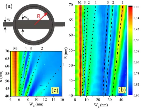
3.1 (a) Sketch of the system under investigation: a quantum ring with average radiusR, attached to input (left) and output (right) channels with the same
width as the ring (W = 10nm), and to an extra horizontal channel of width Wc. (b) Contour plots of the transmission probabilities as a function of the extra channel width and ring radius. The solid, dashed and dotted lines indicate seven minima that are discussed in the text. A zoom of the 4 nm
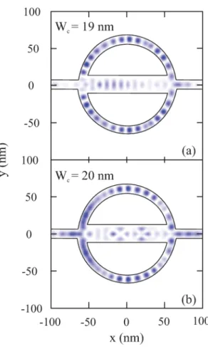
< Wc <16nm region with the logarithm of the transmission is shown in (c). 55 3.2 Snapshot of the propagating wave function at t = 900fs for two values of
the extra channel width: 19 nm (a) and 20 nm (b). . . 57
3.3 Probability density currents as a function of time, calculated (a) in the input lead and (b) in the extra channel, for different values of the extra channel width Wc, for wave packet energyǫ= 70 meV. . . 58 3.4 (a) Eigenstates of a finite quantum well as a function of its width. (b)
Diagram representing the energy sub-bands in the input lead and in the extra channel. The horizontal dotted line is the average energy of the wave packet used in Figs. 3.1 and 3.3, and the shaded area in (a) illustrates the FWHM of the energy distribution of this wave packet. . . 60
3.5 (a) Transmission probabilities as a function of the extra channel width in the vicinity of the minimum labeled asM in Fig. 3.1(a), for several values
of the wave packet energy ǫ = 70 (bottom curve), 80, ... 180 meV (top
curve). The curves were shifted 0.1 up from each other, in order to help visualization. (b) Energy levels (solid) as a function of the channel width, plotted in a log scale, along with two fitting functions (dashed curves), for large (f1) and small (f2) values of the channel width. (c) Numerically
obtained (symbols) positions of the M minima as a function of the wave
xix
3.6 Transmission probabilities for aǫ = 70 meV wave packet scattered by two
kinds of defects in the lead-ring junction: a Gaussian attractive potential of depth VG (solid, bottom axis) and widthσG = 5 nm, and a circular bump of radius Rb (dashed, top axis), which are schematically illustrated in the lower and upper insets, respectively. . . 62
4.1 Sketch of the systems under investigation. (a) Half quantum ring with leads and channel aligned, (b) circular quantum ring with an extra channel in the perpendicular direction, (c) square ring with non-aligned leads and channel, and (d) circular quantum ring with leads and channel aligned. . . 65
4.2 Transmission probability as function of channel width Wc. The frames (a), (b), (c) and (d) refer collectively as the corresponding systems presented in Fig. 4.1. The WP have kinetic energies ε1 (black, dotted line), ε2 (red,
dashed line),ε3 (blue, solid line), propagating in the subband ground state,
while the other is in the first excited state with kinetic energy ε3 (green
dash-dotted line). . . 67
4.3 Time-dependent probability current through the extra channel, calculated for kinetic energy ε1. The different frames refer to the systems in Fig. 4.1. 69
4.4 Snapshots of the squared wave function att = 460fs, for different channel width Wc and kinetic energy ε1. . . 70
4.5 Projection of the wave function on the ground state (top graphics) and first-excited subbands (bottom graphics) as function of channel width Wc, calculated at the output lead. Kinetic energyε1(black dotted line), ε2 (red
short-dot line), and ε3 (blue solid line). This figure is ordered in the same
sequence Fig. 4.1. . . 71
4.6 Contour plots of the transmission probabilities as a function of the extra channel width Wc and magnetic fieldB. This figure is ordered in the same sequence as Fig. 4.1. . . 72
4.7 Transmission probability as function of the channel widthWc for quantum rings depicted in (a) Fig. 4.1(c) and (b) Fig. 4.1(d), respectively. The kinetic energy used was ε1 and each color curve represents a transmission
probability for a specific magnetic field, ranging from 0 (purple) to 1 T (red). 74
4.8 Schematic diagram for an AFM tip potential over quantum rings repre-sented by the dots (1), (2) and (3). The solid arrows indicate the direction of the tip displacement, while the dash line arrows indicate the final posi-tion of the tip. Tip (1) is fixed in the central region for each system. . . 75
xx
5.1 Potential profile scheme for the QWs studied in this work. The two QWs are separated from each other by a distance W2, ranging from 0 to 4.8 nm.
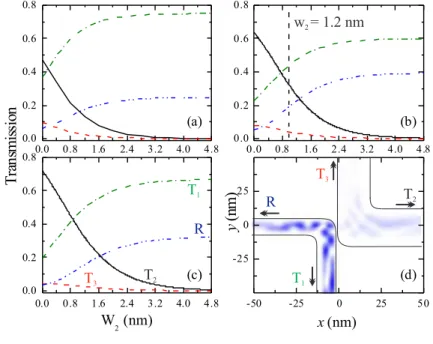
The smooth connections between vertical and horizontal wire are described by circles of radius RW =W1/2 and RL =L/2. . . 80 5.2 (a)-(c) Wave packet transmissions (T) and reflexion (R) probabilities as
function ofW2for a well width ofL=W1. The transmissions are calculated
in three different points in the QWs: bottom T1 (green, dash dot line), top
T3 (red, dash line) right T2 (black, solid line), while the reflexion R (blue,
dash dot dot line) is calculated at the left side, as shown in (d). The wave packet energies used are (a)ε1, (b)ε2 and (c)ε3. (d) Snapshot of the wave
function calculated att = 160 fs forL=W1 and W2 =1.2 nm as depicted
by the vertical dash line in (b). . . 82
5.3 The same result as shows in Fig. 5.2, but now for L= 2W1. . . 83
5.4 Transmission coefficient (T2 + T3) as function of the well widthL, for wave
packet energies (a) ε1 and (b) ε3. Three W2 distance were considered: 0
nm (black, solid line), 1.2 nm (red, dash line) and 2.4 nm (blue, dotted line). 84
5.5 (a) Bottom energy of the different subbands as function of the quantum well width L. Schematic diagrams that represents the subband energies as
function of the wave vector kx in the x direction, for output width of (b)
L= 5 nm, (c)L=10 nm, and (d) L= 20 nm. The horizontal dashed-dot lines represents the average energy of the wave packet, ε1 and ε3.. . . 85
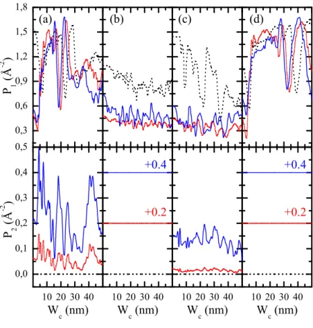
5.6 Projection of the wave function on the ground state P1, first-excited P2
and second-excited subbands P3 integrated in time, for the output width
L = W1, panels column (a) and L = 2W1, panels column (b), as function
of the distance W2 calculated at position 158 nm in the right-lead. . . 86
5.7 The total time-dependent probability current for wave packet energy of ε1
(black, solid line), ε2 (red, dash line) andε3 (blue, dotted line). Results for
different distances W2 are plotted in column (a) W2 = 0 nm, and column
(b) W2 =2.4 nm. The output widthLis in the first rowL=W1/2, second
row L=W1, and third row L= 2W1. . . 87
5.8 Conductance in the output quantum wire as a function of the distanceW2.
Wavepacket energy is ε1 (black, solid lines), ε2 (red, dashed lines) and ε3
(blue, dotted lines) for quantum well L width of (a) 10 nm and (b) 20 nm. 88
5.9 (Color online) Conductance of the quantum wire as a function of kinetic energy wave packet for the three possible output leads G1 (dotted), G2
(solid) and G3 (dashed), with well widths L = 5 nm (blue), L = 10 nm
(black) and L = 20 nm (red). The W2 distance is given by (a) 0 nm, (b)
xxi
6.1 (a) Energy potential ∆Ee(ze) due to conduction band edge descontinuity (red
dashed line) and the potential Σe(ze) due to self-energy corrections (black solid
line). (b) Total potentialV (r) = ∆Ee(ze) +Σe(ze) +Ve−im(r)in thezdirection
(black solid line) and electron ground state wave function (blue dashed line). (c) Coulomb potentialVe−m(r)of electron-impurity interaction in 3D plot. (d) Total
potential V(r) in 3D plot. . . 94
6.2 (Color online) Waves functions projection in the(yz)plane for the ground state, first and second excited states. In (a) the impurity is located inzim= 0nm and
in (b) the impurity iszim= 5nm far from the center of the QW. The z-projection
of the total potentialV(z), in eV, are depicted for QWs with width ofL= 5 nm. 96
6.3 (Color online) Left panels: Electron energy for ground state (black solid line), first (blue dashed line) and second (red doted line) excited state in QW for (a) narrow L = 5 nm QW width and (b) wide L = 10 nm HfO2/GaN QW width.
Right panels: Electron-impurity binding energy for ground state (black solid line), first (blue dashed line) and second (red dotted line) excited state energy as function of impurity position for a (c) narrow (L = 5nm) QW and (d) wide
L = 10 nm HfO2/GaN QW. The dark yellow line-sphere depict the electron
energy (left) and electron-impurity binding energy (right) in narrow (top) and wide (bottom) AlN/GaN QW, and the green dash-dot line shows the effect of the image charges in GaN/HfO2 QW. . . 97
6.4 Schematic diagram of different interactions between electron and their image charges, electron and impurity as well as electron and impurity image charges for GaN/AlN (a)-(c) and in GaN/HfO2 (b)-(d) QWs. In (a)-(b) the impurity is
located in the well region while in (c)-(d) the impurity is located in the barrier region. . . 98
6.5 Electron center-of-mass as function of the impurity position (zim) for (a) narrow
(L= 5 nm) and (b) wide (L= 10nm) QWs. The ground state, first and second excited states are represented by black solid, blue dashed and red dotted lines, respectively. The gray line-sphere depict the standard deviation in position σx
for narrow and wide QWs. . . 99
List of Tables
1.1 - Number and degree of confinement for different degrees of freedom of heterostructures [30] . . . 31
5.1 - Exponential fitting to transmission probabilities T2 shown in Figs. 5.2
1
Introduction
1.1
Brief Historical Overview
In recent decades, technical advances have enabled a large number of experimental studies of semiconductor heterostructures [1, 2, 3, 4, 5]. The pioneers in manufacturing devices based on semiconductors were John Bardeen, William Shockley and Walter H. Brattain, and the transistor they produced is known as the point-contact transistor [6]. Figure 1.1 shows the three researchers (a), the first transistor they developed (b), and the first integrated circuit (c). Through these and other technological advances, we now have extremely efficient electronic devices. Semiconductor devices presents very interest-ing optical and transport properties, which lead to several technological application and represent the vanguard of the electronic devices manufacturing.
Figure 1.1: (a) Scientists John Bardeen (standing left), Walter Houser Brattain (standing right) and William Bradford Shockley (seated); (b) first transistor in history based on semiconductors, manufactured by Bardeen, Brattain and Houser; and (c) first integrated circuit, produced and developed by Jack S. Kilby. Both were invented in the last century [6].
1.2. ENERGY BANDS 24
proposed the fabrication of an artificial periodic structure consisting of alternate layers of two dissimilar semiconductors with layer thickness of the order of nanometers nowadays knows Superlattices. This work enabled numerous subsequent studies that continue to
bring great technological advances.
Techniques such as MBE [2] (molecular beam epitaxy), MOCVD [3] (metalorganic chemical vapor deposition), CVD [4] (chemical vapor deposition) in addition to VLS [5] (vapor-liquid-solid) constitute the vanguard of growth of semiconductor devices, allowing not only the fabrication of Tsu and Esaki’s superlattices, but also artificial lattices of
quantum dots, nanowires and rings [9,10,11,12]. This brought the possibility to observe and control the optical and electronic properties of theses semiconductor nanostructures [13, 14, 15, 16]. Theoretical Ab initio works have also successfully described properties
by ab initial calculations, tight-binding models, k·p Hamiltonians and effective mass
approximation, based on the envelope function [17, 18,19].
1.2
Energy Bands
In order to understand the mechanism responsible for the electrical current in semi-conductor materials and their applications in nanotechnology, a study of energy bands in these materials is necessary. Electrons in an isolated atom are characterized by discrete and quantized energy levels, which correspond to the atomic orbitals 1s, 2s, 2p, 3p, 3d, ... and satisfy the Pauli exclusion principle. In an isolated atom, the calculation is based on the Schrödinger equation, and the solution is exact for low atomic number elements. In a solid, where there is a large number of atoms close to each other, the exact calculation becomes very complicated. This is because the electrons and nucleus of each atom inter-act with the electrons and the nuclei of neighboring atoms. An electron in level 1s in one of these atoms can also occupy this same level in another atom: it will have two distinct wave functions that describe the two possible states, but sharing the same energy, i.e., have a double degeneracy. The degeneracy is “broken” when several atoms are proximate, thereby forming an almost continuous energy band.
Because there are a lot of atoms (N ∼1023cm−3) disposed periodically in the crystal
lattice, energy states are distributed through continuous energy bands, which are sepa-rated from each other by a prohibited zone. The allowed energy states are defined as
energy bandsand the forbidden zone is the gap, as shown in Fig. 1.2.
Semiconductors at 0 K temperature behave as insulators, having all allowed energy states occupied below the Fermi level, while all allowed energy states above the Fermi level are unoccupied1. The lowest energy states are in the so called
valence band, while
the states with the highest energy are in theconduction band. The semiconductor gap
is the energy corresponding to the difference between the top of the valence band and the
1
The Fermi wavelength is given by: λF = 2π/ 3π2n
1/3
1.3. ADIABATIC APPROXIMATION AND EFFECTIVE MASS 25
discrete levels Conduction band
Valence band
Gap
Distance between atoms
Energy
(a)
Conduction band
Valence band
hh lh el
so
<100>
Ex
E(K)
K <111>
G
X L
Eg
ESO
(b)
Figure 1.2: (a) Formation of energy bands due to the approach of a large number of atoms in a solid semiconductor (b)Electron’s energy bands (el), light hole (lh), heavy hole
(hh) and split-off (so) in a semiconductor with gap Eg. The hatched regions illustrate
the occupation of electrons withT > 0K [20].
minimum of the conduction band, and the Fermi energy in an intrinsic semiconductor 2
is the center of the energy gap [20].
Figure 1.2 (a) illustrates the allowed energy states that fills the bands in a semicon-ductor when a large number of ions are made closer. Figure1.2 (b) represents the energy bands as a function of the k wave vector.
1.3
Adiabatic Approximation and Effective Mass
In order to understand the electronic properties of semiconductor materials, it is nec-essary to investigate the behavior of their electrons when subjected to external fields. To describe such many bodies system, we will initially neglect thespin-orbit interaction and
other relativistic contributions [20, 21].
An ideal crystal consists of an infinite set of ions located near the sites a lattice, forming an electron gas that move in the ion field. The basic properties of the crystal depend on the electron dynamics in this lattice and the understanding of this problem depends on the solution of the Schrödinger equation, including electron, electron-ion and electron-ion-electron-ion interactelectron-ions. That allows us to study different aspects of the crystal such as its electronic and ionic dynamics and their interactions with various perturbations, including impurities and external fields.
The complete Schrödinger equation for n electrons and N ions, written in terms of
the electronic coordinates, r1, r2, r3, ..., rn and ionic coordinates R1, R2, R3, ..., RN are:
2
1.3. ADIABATIC APPROXIMATION AND EFFECTIVE MASS 26 " − n X i=1 ~2
2mi∇
2 i− N X k=1 ~2
2Mk∇
2 k+ n X i<j=1 1 4πε0
e2
|ri−rj|
+
N X
I<j
1 4πε0
ZIZJe2 |Ri−Rj|
− n,N X
i,I
1 4πε0
ZIe2 |RI −ri|
#
Ψ (r1, ...,rn, R1, ..., RN) =EΨ (r1, ...,rn, R1, ..., RN), (1.1)
where the first term is the electrons kinetic energy, the second is the kinetic energy of ions, the third is the electron-electron Coulomb interaction potential, the fourth term is the ion-ion Coulomb interaction potential, and the fifth is the potential energy of Coulomb interaction between the electron and the ions. |ri −rj|, |RI −RJ|, |RI −ri|
are, respectively the distances between the electroni and the electronj, ionI and ion J, and between the ionI and the electron i.
As the electron mass is less than the ion mass by a factor of approximately 1/1800
(mi ≈ 1.8×10⁻³MI), the electron’s kinetic energy is much higher than that of the ions.
The electronic distribution continually adjusts itself with the positions of the ions, which at any time can be considered the same. This suggests that the ions remain approximately at rest. This hypothesis is called adiabatic approximation (Born and Oppenheimer 1927) [22]. It can be expressed by writing the wave function Ψ (r1, ...,rn, R1, ..., RN), where
electron coordinates are collectively represented byrand the ionic coordinates collectively represented byR:
Ψ (r,R) =ψ(r,R)ϕ(R), (1.2)
where ψ(r,R) is the electronic eigenfunction, which depends on the coordinated r of
electrons and coordinate R of ions, appearing as a fixed parameter. This eigenfunction
satisfies the Schrödinger equation :
" − n X i=1 ~2
2mi∇
2 i− n X i<j=1 1 4πε0
e2
|ri−rj| − n,N X
i,I
ZI
4πε0
e2
|RI −ri| #
ψ(r,R) =Ee(R)ψ(r,R),
(1.3)
whereEe(R)is the electronic eigenvalues, which depend on the coordinate R. The
func-tion ϕ(R) is the ionic eigenfunction and satisfies
" − N X I=1 ~2
2MI∇
2
I + Φ (R) #
ϕ(R) =Eϕ(R), (1.4)
1.3. ADIABATIC APPROXIMATION AND EFFECTIVE MASS 27
Φ (R) =Ee+ N X
I<j
ZIZJ
4πε0
e2
|Ri−Rj|
(1.5)
is the effective potential energy of the ions andE is the total energy. Eq. 1.4 is the ionic Schrödinger equation and arises from the substitution of eq. 1.2 in eq. 1.1.
The ionic coordinates R in eq. 1.4 are arbitrary. Nevertheless, if ions occupy the
equilibrium positionR0 of the crystal structure, the electron-ion interaction potential
be-comes periodic, with the same periodicity as the crystal lattice. The number of terms in eq. 1.4 is much smaller that in Eq. 1.1; however, even with the adiabatic approximation, the exact solution of eq. 1.3 is not possible. We then consider that electrons are indistin-guishable and independent particles and that each electron moves under the influence an average potential Vcr(r), which describes the electron-ion interactions. Thus, the motion
of a single electron can be described by the Schrödinger equation:
p2
2m0
+Vcr(r)
ψn,k(r) = En,kψn,k(r). (1.6)
In an ideal crystal structure, the potential Vcr(r) is periodic, and the wave function
describes a Bloch state:
ψn,k(r) = eikrun,k(r), (1.7)
whereeik.r is a plane wave function, andu
n,k(r) is a Bloch function, which has
periodic-ity of the crystal lattice (un,k(r) =un,k(r+R)) and describes the behavior of the wave
function within an unit cell. Substituting eq. 1.4 in eq. 1.3, we have:
H un,k(r) =En,kun,k(r), (1.8)
where we identify the Hamiltonian as
H=
− ~
2
2m0∇ 2+V
cr(r) + ~2k2
2m0
+ ~
m0 k.p
. (1.9)
If we take the center of the Brillouin zone, at the point Γ(k =0), the solution to eq. 1.8
form a complete set of functionun,0(r) (for n=1,2,3,...) which allows us to calculate the
wave function for anyk6= 0 as a linear combination of Bloch functions.
un,k(r) = ∞ X
n′
cn,n′un′,0(r), (1.10)
1.3. ADIABATIC APPROXIMATION AND EFFECTIVE MASS 28
As our interest is focused on the study of electrons that are located in the conduction band, which is quite far from the valence band (except for narrow gap semiconductors which are not investigated here) we can simplify the model by considering a single of a band. The wave function of an excited state of an electron in the conduction band is formed by a Bloch function and the corresponding envelope function. In this way thek·p
Hamiltonian is expanded into a basic element given by eq. 1.10
hun,0|Hkp| un,0i=En,0+
~2k2
2m∗ i
, (1.11)
This model leads to a form of energy dispersion occurring in the equivalent model of free electrons, or conduction band region near the pointk =0 is approximately parabolic
shape. However, the curvature differs from that of the parabolic free electrons dispersion, and depends on the specific composition and structure of the semiconductor. This curva-ture is introduced by means of an empirical parameter called effective mass (m∗
e), which
can be calculated by applying perturbation theory to thek·p Hamiltonian. In this sense,
the unperturbed Hamiltonian and the perturbative term are defined, respectively, as
H0 =−
~
2m0∇ 2 +V
cr(r), (1.12)
and
H′
= ~
2
2m0|
k2|+ ~
m0
k·p, (1.13)
The energy En,k, corrected up to the second order, is given by:
En,k =En,0 +
X
α=x,y,z ~2kα2
2
"
1
m0
+ 2
m2 0
X
n′ Pα
n,n′ 2
En,0−En′,0 #
, (1.14)
where the termPα
n,n′is an empirical parameter determined either experimentally or by first principles calculating, and the term in brackets, identified as the inverse of the effective mass, can be condensed as
1
m∗ =
1
m0
+ 2
m2 0
X
n′ Pα
n,n′ 2
En,0−En′,0
. (1.15)
Thus, the energy obeys
E(k) = En,0+
~2k2
1.3. ADIABATIC APPROXIMATION AND EFFECTIVE MASS 29
Therefore, in the case of an infinite periodic crystal, which has no confining direction (Bulk), the envelope function of the conduction band is a plane wave, according to the Bloch theorem, eq. 1.7. From the point of view of kinematics, a Bloch electron, has acceleration given by:
ak = ∂vk
∂t =
1
~
∂
∂t[∇kE(k)],
ak =
1
~
∂ ∂t
∂E(k)
∂p , (1.17)
where we use the relation vk = ∇kωk = 1~∇kE(k), that is, the electron velocity in the state k is equal to the gradient of the energy band in reciprocal space. The acceleration
can be rewritten as:
ak =
1
~
∂ ∂t
∂E(k)
∂k dk
dt =
1
~2
∂2
∂ki∂kj ·
F, (1.18)
where we use p = ~k and F = dp/dt = ~dk/dt. Comparing the latter equation with
Newton’s second law, we have:
F=~2
∂2E(k)
∂ki∂kj −1
a. (1.19)
so that the effective mass can be expressed as:
m∗ i,j =~2
∂2E(k)
∂ki∂kj −1
. (1.20)
Eq. 1.20 is the effective mass tensor for an electron band, whose components are:
1
mi,j
= 1
~2
∂2E(k)
∂ki∂kj
, (1.21)
Thus, a Bloch electron excited by an external force field behaves as if it had an anisotropic mass, that differs from the free electron massme. The effective mass
implic-itly incorporates all the information about the lattice structure that leads to the energy band E(k). For some crystals, non-diagonal components of the effective mass tensor are
nonzero. Thus, an applied electric field in a certain direction of the crystal can cause electron acceleration in a different direction. In most semiconductors the effective mass tensor is diagonal and in isotropic crystals in particular, the tensor reduces to a scalar:
m∗
= ~
2
∂2E(k
)/∂k2
1.4. THE ENVELOPE-FUNCTION APPROXIMATION 30
Note that the valence band normally has three branches, called light hole, heavy hole and split-off, due to their different effective masses, as one can see in Fig. 1.2(b). The theoretical expressions found for the electrons effective mass are also valid for holes, and in general, their values change as the crystal structure, periodicity of the lattice and the chemical composition of the material. Within the so-called effective mass approximation, the electrons (holes) in the conduction (valence) band of a material are considered as free moving particles, where the influence of any external potential is added to the effective continuum model Hamiltonian, and interactions with other electrons and lattice ions are all taken into account by introducing of the effective mass3
1.4
The Envelope-Function Approximation
The envelope-function approximation is a mathematical formalism which allows the use of the effective mass approximation to study heterostructures materials, through the Hamiltonian
H= p
2
2m∗ +V(r). (1.23)
The method assumes as an approximation that all materials constituting the het-erostructure have similar type of crystalline lattice and similar network structure so that we can assign the same Bloch function on the entire system.
In this work, we use the effective-mass approach, which considers a crystal infinite size. For calculation purposes, we will now consider limited heterostructures nanoscale sizes, because when we consider that the system is limited by the crystal size, the electron is also confined within the limits of this heterostructure. This is what divides the quantized energy spectrum into discrete levels at the bottom of the conduction band. The spatial confinement potential is defined by V(r), which in turn is defined by the energy bands
mismatch between materials forming the heterostructure.
A great advantage of using these approximations is in the fact that they simplify the inclusion additional perturbations, such as electric or magnetic fields, in the theoreti-cal description of the charge carriers dynamics. This task often resorts simply to the introduction of an extra potential term in the Hamiltonian of eq. 1.23 [22,23, 24].
1.5
Low-Dimensional Semiconductor Systems
It is impossible to think of modern physics or solid state physics and not to refer semiconductor heterostructures, particularly quantum wells, wires and dots [25]. The
3
1.5. LOW-DIMENSIONAL SEMICONDUCTOR SYSTEMS 31
possibility of nanomanufacturing these devices was the fundamental piece for numerous articles published since the 70’s [7, 8].
The carriers confinement potential in these systems arises from the mismatch between the energy bands in the heterostructures, since the heterostructure materials are separated by different gaps and different electronic properties, such mismatch attracts carriers to the region where the potential is lower. The fraction of the difference between the gaps which is responsible for confining electrons, is called conduction band-offset. The band-offset is a parameter usually obtained from experimental results, but it can also be calculated by means of the electron affinity, using the vacuum level as reference[20].
The carriers confinement can occur in one, two or three dimensions, as shown in Table 1.1 where the mathematical rule Gconf +Gf reedom = 3 is kept. In one dimensional
confinement, the system has two degrees of freedom (2-D), as in quantum wells; in two dimensional confinement, electrons are free to move only in 1-D, such as in quantum wires, or nanowires. Finally, when there is confinement in all directions, the carriers have zero degrees of the freedom, 0-D, as in quantum dots, which are sometimes called artificial atoms [31].
Table 1.1: - Number and degree of confinement for different degrees of freedom of heterostructures [30]
System Gconf Gf reedom
Bulk 0 3
Quantum Wells 1 2
Quantum Wires 2 1
Quantum Dots 3 0
1.5.1
Quantum Dot
Quantum dot is a semiconductor structure with a size comparable to the Fermi wave-length. Its charge carriers are confined in all directions, so that electronic states are fully quantized [32]. Quantum dots are also known as artificial atoms because their electronic behavior is similar to that of an atom, but differs regarding the potential: in the the case of a quantum dot, the potential is step-like, while for the atom, the potential is Coulombic [30]. Recently, self-organized quantum dots have been grown by the Stranski-Krastanow method [33]. Quantum dots grown using this technique have the symmetry of a semi-ellipsoid, where the deposited materials are grown from the bottom up. Fig. 1.3 shows three quantum dots grown by the self-assembly process.
1.5. LOW-DIMENSIONAL SEMICONDUCTOR SYSTEMS 32
Figure 1.3: Micrograph image obtained by scanning an electron to three types of quantum dots: circular, square and triangular, manufactured by self-assembly method [36].
widely used in theoretical works [34, 35]. This implies that the energy spectrum in the z direction have energy levels transitions with higher energy than those in the(x, y)-plane.
In this way, we justify the study of the electronic behavior only in the (x, y)-plane, saving considerable computational time to obtain results.
1.5.2
Quantum Wires
Wires with diameters of a few nanometers, which can be considered effectively as 1-D structures have been recently manufactured [37,38] and studies of carriers (electrons and holes) confinement effects have been demonstrated with different levels of sophistication [15, 18, 39, 40]. For application as non-volatile memories, Zhu et al [13] have recently shown that silicon nanowires (Si) surrounded by a dielectric with high constant dielectric (high-k dielectric), as shown in Figure 1.4, exhibit excellent recording operations and good resistance. This shows that materials with high dielectric constant, growing around low-dimensional structures continues to attract the attention of researchers in order to extend Moore’s Law [41].
Silva et al [15] presented a study of excitons properties in cylindrical nanowiresSi1−xGex
surrounded by a silicon matrix, assuming the two known forms of band alignments, namely type-I and type-II 4. The method used by the authors is based on the effective mass and
envelope function approximations. Actually in general, theoretical studies on this subject are based on: (i) the use of the effective mass approximation, (ii) self-consistent solution of the Schrödinger and Poisson equations in cylindrical coordinates, providing theoretical descriptions of electronic and optical properties of the quantum wires [15]; (iii) methods based on first principles calculations (ab-initio methods) [45], which require high compu-tational cost and, therefore, are limited for studies of nanowires with diameters between
4
Regarding the type of quantum wires, they may be classified as type-I or type-II. When the alignment of the bands occurs in such way that in the same layer we have a quantum well both for electrons and for holes, this configuration presents features of type-I. But in case that we do not have this type of alignment, i.e. when the electrons and holes are confined in different semiconductor layers, the potential
1.5. LOW-DIMENSIONAL SEMICONDUCTOR SYSTEMS 33
c
D
Figure 1.4: Quantum wires (a) SEM’s image for the GaAs material with wire radius 50 nm grown with LCG techniques, [37](b)SEM image for the GaP material with radius 50 nm grown with LGC techniques, [37] (c) TSEM Image for AlGaAs nanowire perpendic-ular growth of Al, Ga, As and O, respectively, reference bar equals 50 nm grown with techniques MBE, [38] and (d)AFM image of a Si nanowire on the Au substrate with radius
10nm grown with techniques VLS, [47]
1 and 2 nm; (iv) tight-binding, Approximating the electronic wave functions in the solid by linear combinations of the atomic wave function, this approach is known as the tight-binding approximation or Linear Combination of Atomic Orbitals (LCAO) approach [46], and (v)k·p, the pseudopotential method is not the only method of band structure
calcu-lation which requires a small number of input parameters obtainable from experimental results. In the empirical pseudopotential method the inputs are usually energy gaps. The k·p method can be derived from the one-electron Schrodinger equation. Using the Bloch theorem the solutions are expressed, in the reduced zone scheme [46]
1.5.3
Quantum Wells
If the nanostructure is composed of a thin semiconductor layer, grown by epitaxy be-tween two layers of different alloy, a confining potential∆E appears in only one direction, as shown in Fig. 1.5, due to the bands mismatch between the materials. This formed nanostructure is called quantum well.
1.5. LOW-DIMENSIONAL SEMICONDUCTOR SYSTEMS 34
AlGaAs GaAs AlGaAs
z
x
y
I
II
I
D
E
z
0 w
Figure 1.5: Physical structure of a quantum well of AlGaAs/GaAs and representation of the potential profile of this heterostructure. In the right side, (I) represents the alloy AlGaAs and (II) represents the GaAs.
the development of the heterostructures by Esaki and Tsu. This is due to their great po-tential for technological application and the countless physical properties they can provide, such as interband electronic transmission, excitonic properties, electron correlation of the charge carriers, strain-induced properties, among other various possibilities [48, 49, 50]. Besides, quantum well heterostructures require one of the less complex growth procedure, facilitating research in experimental laboratories [51,52]
The achievement of a sharp interface imposes very stringent requirements on the growth conditions, such as purity of the source materials, substrate temperature and many others too numerous two dissimilar materials A and B, known as a heterojunction, is determined by their chemical and physical properties [46].
1.5.4
Quantum Rings
Quantum ring nanostructures regarding confinement dimensions are similar to quan-tum dots, but they have very interesting properties coming from their topology that allow, for example, experimental observation of the Aharonov-Bohm effect [53]. One method of growing quantum rings is through anodic oxidation. (See Fig 1.6). The anodic oxida-tion is oxidaoxida-tion by applying a potential difference between the probe of an atomic force microscope and the sample [54]. Another way of fabricating a quantum ring consists of quantum annealing (annealing) of a self-grown quantum dot, which causes a slippage from its center, thus forming the ring.
1.6. THE AHARONOV-BOHM EFFECT 35
Figure 1.6: (a) Image obtained by atomic force microscopy (AFM) of a quantum ring grown with the anodic oxidation technique, (b) experiment the potential profile, where the dark curves represent the oxides lines [55].
1.6
The Aharonov-Bohm Effect
We will discuss in our work the problem of an electron in a quantum ring under the influence of an external magnetic field, so it is necessary to briefly overview the Aharanov-Bohm effect, which has been discussed widely in recent years for systems with cylindrical symmetry [56, 57, 58].
Path
1
Path
2
B 0¹
screen
Electron
Figure 1.7: Illustration of experience proposed by Aharonov-Bohm. Between two slits a magnetic field B is applied. It is different from zero only in the inner region of the applied field, but the vector potential (shown by solid lines) is different from zero in all space, with cylindrical symmetry causing opposite effects on the path 1 and 2.
Figure 1.7 illustrates a scheme of the Aharanov-Bohm gedanken experiment. The
1.6. THE AHARONOV-BOHM EFFECT 36
pattern. Between the two slits is placed a cylindrical coil (permanent magnet or solenoid), that generates a magnetic field B only inside it. The possible electron paths are in the
region where the field is zero.
Even in the absence of magnetic field in the path where the electrons pass, there is a potential vectorAin this region given by: B =∇ ×A = 0, causing the momentum of the
electron to assumep→p−qA. Taking the magnetic field of the material asB=Bbk, the vector potential can be expressed by a symmetric gaugeA= 12Bρbeθ. Observing Fig. 1.7,
the vector potential points to the same direction as path 2, and in the opposite direction to path 1. This implies that the electrons that pass by 1 will have their momentum p
different from electrons that pass by 2; this fact changes the interference pattern generated in the screen. This difference observed in the screen due to the application of the external magnetic field is know as Aharanov-Bohm effect (AB) [59, 60].
In this approach, we have chosen a potential vector with a specific gauge; however, more extensive descriptions show that this effect does not depend on the choice of the gauge, for the vector potential [27, 29,46, 60].
Further in this thesis, we will investigate fluctuations in transmission probabilities of an electron in a quantum ring under an external magnetic field applied perpendicular to its plane direction (x, y), where such AB effect is expected to occur. When the magnetic flux located between paths 1 and 2 reaches the value of φ = (n+ 0.5)φ0 , where n is
an integer and φ0 = h/e is the elementary flux, wave functions following different paths
interfere in the area of the ring-leads junctions and undergo a destructive interference, causing a lower electronic transmission. Thus we can see that the transmission in terms of the magnetic flux has a frequency φ0 , presented here as AB oscillations [61]. In an
actual nanodevice, at low temperatures, the inelastic scattering length is much larger than the sample dimensions and, as a result, the transport is completely phase coherent, i.e., it is dominated by quantum interference effects, allowing for experimental observation of the AB oscillations. On other hand, at very high temperatures, the inelastic scattering length is much smaller than the sample size, which brings the system back to the classical behavior, thus losing the interference effects. [62, 63]
Interestingly, the AB phase also have strong influence in the energy spectrum of a quantum ring. Let us consider an electron in planar ring system, which is infinitesimally small in the z-direction, so that only one bound state in this direction plays a role. We can write the Hamiltonian of this system as
H = P
2
2m∗, (1.24)
as previously defined using the momentum modified by the magnetic field: P−qA we have:
H= (P−qA) 1
2m∗ (P−qA), (1.25)
1.7. BRAESS PARADOX AND GAME THEORY 37
H = 1
2m∗ P
2+ 2eA
·P+e2A·A, (1.26)
taking a symmetric gauge for the vector potentialA = 0.5Bρeθ, we have for each term of
eq. 1.26:
P2
2m∗(R) =− ~2
2R ∂ ∂R
R m∗(R)
∂ ∂R
− ~
2
2m∗(R)R2
∂2
∂R2 (1.27)
1 2m∗
(R)(2eA·P) =
~
i eB
2m∗
(R)
∂
∂θ (1.28)
and finally:
e2A·A
2m∗(R) =
e2B2
8m∗(R)R
2 (1.29)
Replacing the eqs. 1.27, 1.28 and 1.29 in 1.26 and taking only the radial terms, we have:
H=− ~
2
2m∗(R)R2
∂2
∂θ2 +
~ωc
2i ∂ ∂θ +
1 8mω
2
cR2, (1.30)
where ωc = eB/m∗ is defined as frequency cyclotron and m∗ is effective mass of
elec-tron. Using the definition of elementary magnetic flux and magnetic flux, we write the Hamiltonian of eq. 1.30 as:
H=− ~
2
2m∗R2
−i ∂ ∂θ +
φ φ0
2
. (1.31)
The eigenfunctions for the Hamiltonian of eq. 1.31 are written as:
ψ(θ) = exp (inθ)
2√2π , (1.32)
wheren = 0,±1,±2, ... and eigenstates are obtained:
En(φ) = ~2
2m∗R2
n+ φ
φ0
(1.33)
from eq. 1.33we can see that energy is a function of magnetic flux and has a parabolic shape having minimum atφ =−nφ0. Thus, we can conclude that there are fluctuations
AB with period φ0, and that there is an exchange of angular momentum in the ground
state to flow inφ= (n+ 0.5)φ0.
1.7
Braess paradox and game theory
1.7. BRAESS PARADOX AND GAME THEORY 38
common sense that adding extra paths should always improve the flow, and appear to be similar to the Braess paradox in game theory. In order to understand this paradox, it is necessary to review some concepts of game theory.
John Nash, in the mid 1950s, proposed a theory for n players, each with i possible
moves, in which there is at last one equilibrium point satisfying all players. This point is known as Nash equilibrium, and presents applications in economic science and game theory[66]. Conceptually, the ideal game is one where no player receives incentive to change strategy after the opponents have made their choices, so that no other strategy taken by any player after this point will result in benefit. Even for players that do not cooperate, it is possible to individually find the best strategy for the game, leading to stability, provided there is no incentive for players to change their behavior. This possibility stems from the predictions that the players can make about the behavior of their opponents. Thus, the Nash equilibrium corresponds to a combination of strategies so that each player makes the best possible move for him(her)self, taking into account the strategy chosen by the opponents. In this context, the result pleases all players, so that none of them have an incentive to change the initiated strategy [66]. In general, the Nash equilibrium is achieved when the system is in a Pareto optimal. The Pareto optimal occurs when there is no way to improve the payoff of one of the players without reducing the payoff of another player; for example, when Companies A and B sell different products on the market in a way that the sale of each of their products do not affect the final corporate profits [67, 68].
The Braess paradox is credited to German mathematician Dietrich Braess. In his publication in 1968s, he concludes that the addition of an extra path in a traffic network can, in some situations, reduce the overall flow. This is a situation where the system can be in a Nash equilibrium, but out of Pareto optimality [69].
As an example, suppose that people have to travel in a road from point A to point B, with two possibilities to perform this activity, see Figure1.8. Each individual chooses a route minimizing the traffic time between the inlet and the outlet, which, of course, depend on the number of people going through a given route. Equilibrium occurs when time is equal for both routes. This case would be the one where there is the same amount of people passing through each path. Let us now discuss this situation in terms of game theory. In the case of Figure1.8, definingfas the relative frequency of people who decided to go by a given path, we can take a fixed time t, representing the time required to pass through the parts of the roads where flow does not depend on the amount of players who pass through it, and t′
= f t and t′′
= (1−f)t, representing the times necessary to go
through the parts of the road where flow depends on the amount people passing through it. Total travel time for the upper (lower) path is Tu = t+t′ (Tl = t+t′′). Thus, the
1.7. BRAESS PARADOX AND GAME THEORY 39
A
B
t’ = f
t
t’’ = (1-f)
t
0.1t
(a)
(b)
t
t
A
B
t’ = f
t
t’’ = (1-f)
t
t
t
Figure 1.8: Scheme to the paradox of Braess (a) A network paths systems starting at point A and ends at point B and (b) Systems paths adding an extra path in the central region with fixed time in extra path.
(ii) lower path is the best if t +f t ≥ t+ (1 −f)t, i.e. if f ≥ 1/2. But if f < 1/2,
everybody will seek for the upper path (supposed to be the best), so f → 1, leading to
Tu =t+t= 2t and Tl =t < Tu, which is inconsistent with the idea that the upper path
is the best. Similar conclusion is drawn for f >1/2, were f →0. Therefore, equilibrium
situation is attained only iff = 1/2and everybody gets a delayTu =Tl=t+ 0.5t = 1.5t.
Now, let us add an extra road with fixed time 0.1t connecting the pathways in the central region, which would allow an escape route between upper and lower paths. Com-mon sense would say that more options means better results. However, taking up-per path until the end, one gets f t + t delay; but taking the extra path, one gets Textra = f t+flt + 0.1t = 1.1t (fl is the fraction of players that change to the lower
path) or even a bit less, if not everybody takes the extra path. It turns out this is always better than Tu or Tl, since, if one takes first the upper path, one is left with a variable
component flt+ 0.1t, which is, at most, 1t+ 0.1t = 1.1t < 1.5t. But then, everybody
will take this path, since this is a dominant strategy - it willalways lead to better results
for each individual than the other options. In this way, everybody makes the same move, f = fl = 1 and finally Textra = 2.1t, which is larger than the 1.5t we had before the
1.8. QUANTUM WIRE DEVICES 40
the overall flow depends on the strategy of players and not just the addition of an extra route [70, 72].
1.8
Quantum wire devices
Modern technology is characterized by its on miniaturization. These reductions in the size are made up to the nanoscale, which is useful in the development of modern transistors. With that, it is possible to increase the number of transistors that fit into a chip-set. Gordon Moore, co-founder and current director emeritus of Intel, made a prediction in 1965 that every two years, the increase in computer processing power would double, this led him to predict that this trend should be continued over the years. This fact became known as Moore’s law. Today, we observe that these values are doubling (in average) every eighteen months [41, 73]
Figure 1.9: (a) A scanning electron micrograph of a 2µm× 2µmsilicon nitride paddle. The supporting rods are 230 nm wide and 3 µm long, and the thickness of the device layer is 240 nm. (b) A scanning electron micrograph of silicon nitride suspended wires. The length of the wires varies form 1 to 8µm. Adapted from [78].
Nowadays, manufacturing of nano-devices is fundamentally based in semiconductors heterostructures, such as quantum wires and quantum dots - specifically, the former have electrons free to move in one-direction and is especially important on the field of medical, optoelectronic applications, di-electrophoretic manipulation and photovoltaics devices [74,
1.9. OUTLINE OF THIS THESIS 41
silicon nitrade was deposited on it, by low-pressure chemical vapor deposition (LPCVD) [78]. In this context of smaller and smaller semiconductor devices, quantum tunnelling between electronic pathways becomes an important topic of discussion, which can be investigated by wave packet propagation and scattering, as we will demonstrate further in this thesis.
1.9
Outline of this thesis
In chapter 1 we have introduced briefly some historical facts about the discovery
and manufacturing of semiconductors nanostructures and their relevance in condensed matter physics and new technological applications. We discussed about energy bands and the approximations used in this thesis. We described the must important low-dimensional semiconductors systems, such as, quantum dots, quantum wires, quantum wells and quan-tum rings.
In the chapter 2 we give a brief introduction to the calculations tools used in this
thesis, specially the so called Split-operator technique. In this chapter, we show how calculate the propagation using this method and how it is adapted for computational codes. Using real time propagation, we calculated the transmissions probabilities and the currents on system. Finally, we discuss over imaginary time evolution, the technique that was used on the fourth work of this thesis.
In thechapter 3we theoretically demonstrate that the transport inefficiency recently
found experimentally for branched-out mesoscopic networks can also be observed in a quantum ring of finite width with an attached central horizontal branch. This is done by investigating the time evolution of an electron wave packet in such a system. Our numerical results show that the conductivity of the ring does not necessary improves if one adds an extra channel. This ensures that there exists a quantum analogue of the Braess Paradox, originating from quantum scattering and interference.
In the chapter 4We theoretically investigate the effect of opening and closing
path-ways on the dynamics of electron wave packets in semiconductor quantum rings with semi-circular, circular, and squared geometries. Our analysis is based on the time evolu-tion of an electron wave packet, within the effective-mass approximaevolu-tion. We demonstrate that opening an extra channel in the quantum ring does not necessarily improve the elec-tron transmission and, depending on the extra channel width, may even reduce it, either due to enhancement of quantum scattering or due to interference. In the latter case, transmission reduction can be controlled through the Aharonov-Bohm phase of the wave function, adjusted by an applied magnetic field. On the other hand, closing one of the channels of the branched out quantum ring systems surprisingly improves the transmission probability under specific conditions.
In the chapter 5 we theoretically investigate the electronic transport properties of