Control of Distributed Power Flow Controllers
using active power from homopolar line currents
Ivo M. Martins
*, Fernando A. Silva
**, Sónia F. Pinto
**, Isménio E. Martins
**CIEEE, Department of Electrical Engineering, ISE, University of Algarve, Faro, Portugal **CIEEE, Department of Electrical and Computer Engineering, IST, TU Lisbon, Portugal
Abstract – Flexible AC Transmission Systems (FACTS)
devices can be used for power flow control in AC transmission grids, improving power line utilization and performance. Nowadays, Unified Power Flow Controllers (UPFC) are one of the most useful FACTS, allowing the simultaneous control of the bus voltage and line active and reactive power. However, due to high costs and reliability concerns, the utilization of this technology has been limited in such applications.
The concept of Distributed FACTS (DFACTS) and Distributed Power Flow Controller (DPFC) was recently introduced as a low coast alternative for power flow control. This paper presents a distributed power flow controller that uses third-harmonic frequency currents transmitted through the line to independently control active and reactive power flow at fundamental frequency.
Simulations were carried in the Matlab/Simulink environment.
Index Terms – FACTS, DFACTS, UPFC, DPFC, Power
Flow Control.
I. INTRODUCTION
All over the world electric power supply systems are widely interconnected, involving national and international connections. This is done for economic reasons, to reduce the price of electricity, but mainly to increase the capacity and reliability of the electrical energy supply. Interconnections between transmission networks can take full advantage of the availability of electricity production systems, depending on the diversity of the load, and minimize also the costs of energy production, maintaining stability.
Although energy transmission is often an alternative to the implementation of new energy production systems, the costs of transmission lines, losses associated with energy transmission and the difficulties to obtain new corridors limit the available transmission capacity. Moreover, the introduction of renewable energy has brought an increasing number of probabilistic variables to the electrical system, since the production of electricity became uncertain and less controllable. This uncertainty in production also leads to an uncertain power flow in transmission lines. Thus, it became essential to improve the performance of power lines and the optimization of power flow on existing lines.
The development of new technologies based on power electronic converters allows a solution for these problems, offering the possibility of power flow control
both in static and dynamic conditions, making the transmissions systems more flexible. FACTS devices can be inserted in existing transmission lines to achieve control functions, including enhancement of power transfer capacity, decrease line losses and generation costs, and improve the stability and security of the power system [1,2]. The Unified Power Flow Controller is a third generation FACTS system and is the most powerful FACTS device currently. It uses solid state power semiconductors and can be used for power flow control, improvement of transient stability, damping oscillations and active filtering [3]. In most recent research works, the UPFC is primarily used to control a local bus voltage and active and reactive power flows of a transmission line. However, in practice, the UPFC series converter may have other control modes such as direct voltage injection, phase angle shifting and impedance control modes, [4].
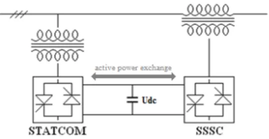
The UPFC is the combination of a Static Synchronous Compensator (STATCOM) and a Static Synchronous Series Compensator (SSSC), coupled via a common DC link allowing active power exchange between the two converters. The converter in series with line acts as a synchronous ac-voltage source and provides the main function of the UPFC by injecting a controllable voltage vector. The shunt converter acts as a synchronous source controlling the voltage of the dc capacitor (Udc). Fig. 1 illustrates the simplified diagram of UPFC.
Figure 1 – Simplified diagram of UPFC
Typical FACTS devices can operate at up to 345 kV and can be rated as high as 200 MVA. Even though FACTS technology is technically proven, it has not seen widespread commercial acceptance due to a number of reasons [5,6]: i) High system power ratings require the use of custom high power devices; ii) High fault currents and basic insulation requirements stress the power electronics system; iii) Utilities require higher reliability levels than what they have so far experienced with FACTS devices; iv) Required skilled work force in the
field to maintain and operate the system; v) High total cost of ownership.
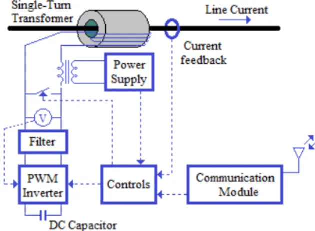
For a lower cost and higher reliability the concept of distributed FACTS devices has recently been proposed as an alternative approach for realizing the functionality of FACTS devices [5,6,7,8]. Currently, the presented DFACTS device is the Distributed Static Series Compensator (DSSC), presented in Fig. 2. Since the DSSC has no power source, it can only adjust the line impedance, and is not as powerful as UPFC.
Figure 2 – Circuit schematic of a DSSC module
To obtain the functionality of UPFC using the concept of DFACTS devices, a new concept of distributed power flow controller (DPFC) that combines conventional FACTS and DFACTS has already been proposed [9]. The DPFC is derived from the UPFC but eliminates the common DC link between the shunt and series converters. The same as the UPFC, the DPFC gives the possibility to control system parameters, such as line impedance and power angle.
This paper presents the controller for a distributed power flow controller able to control active and reactive power flow in static and dynamic conditions. Third-harmonic currents injected into the line provide active power for the DPFC to control active power flow at fundamental frequency.
To test the designed controller, switching models were built in Matlab/Simulink environment. Some simulation results are presented and discussed.
II. DISTRIBUTED POWER FLOW CONTROLLER
The DPFC uses multiple small-size single-phase converters, distributed in series with the transmission line, to inject a relatively small controllable voltage vector to vary the transmission angle and line impedance, allowing cross-coupled control of active and reactive power flow. The use of a large number of DPFC devices provides increased system reliability due to redundancy of the series converters. Each converter within the DPFC is independent and has its own dc capacitor to provide the required dc voltage. Fig. 3 shows the configuration of a transmission line with DPFC devices.
Figure 3 – Transmission line with DPFC devices
To provide independent control of active and reactive power (as in the UPFC) it is necessary to supply active power to all DPFC devices, to maintain the voltage of the dc capacitor (Udc). So, in order to eliminate the common DC link of UPFC, in this paper it is proposed that the required active power is transmitted to all devices through the line at third-harmonic frequency. Once the active power at different frequencies is isolated from each other, it is possible to DPFC devices to absorb active power at third-harmonic frequency and release it at the fundamental frequency. Fig. 4 illustrates the power flow diagram in a transmission line with DPFC devices. As can be seen each DPFC device handles active and reactive power at fundamental frequency and active power at third-harmonic frequency.
The required active power needed by DPFC devices can be supplied by a conventional controlled voltage source shunt converter, as described in [9], represented in Fig. 4 as a third-harmonic current source (I3h).
Figure 4 – Power flow diagram
As illustrated in Fig 4, the transmission line carries both the current at fundamental and third-harmonic frequency. In order to block the harmonic which carries the active power transmitted to DPFC devices, zero sequence harmonic is selected, since the most widely used transformer in power systems is Y-Delta transformer, which has the capability to block the zero sequence component naturally, preventing the harmonic leakage to the rest of the network.
A. DPFC Converter Model
The DPFC converter topology presented in Fig. 5 uses three single-phase half-bridge legs sharing a common dc bus subdivided by two capacitors (C1 and
C2). The voltage across each capacitor is approximately half of the dc voltage bus (Udc), allowing each converter leg to deliver one of two possible voltages levels Udc/2
(Uc1) or –Udc/2 (–Uc2) between its output and the converter neutral point (vok).
Figure 5 – DPFC converter topology
Switching Variables
Assuming semiconductors as ideal switches, each converter leg can be represented by the switching variable γk (k ∈ {1,2,3}), and each switch represented by
the control variable Ski. Each switch has two possible states, on (Ski=1) or off (Ski=0), allowing two possible switches states combinations to produce the two different voltage levels in each leg (Table 1).
Table 1 – Single-phase half bridge converter voltage levels and corresponding switch states
γk Sk1 Sk2 vok
1 1 0 UC1
0 0 1 -UC2
To guarantee the topological constraints of this converter, for each leg the switching strategy must ensure complementary states between switches pairs:
1 2
k k
S
=
S
(1)According to restrictions (1), the switching variable
γk can be defined as:
1 2 2 1 1 ( ) 0 k k k k k if S ON and S OFF t if S ON and S OFF γ = (2) State-Space Model
Analyzing the converter in Fig. 5, the vok voltage and
Ik and I’k currents can be represented as function of the γk switching variable. 1 2
1
0
k ok kUc
if
v
Uc
if
γ
γ
=
=
−
=
(3)1
0
k k0
k ki if
I
if
γ
γ
=
=
=
(4) '0
1
0
k k k kif
I
i if
γ
γ
=
=
−
=
(5)Voltage vok equations and Ik and I’k currents can be rewritten as: 1 2 . ( 1). ok k k v =
γ
Uc +γ
− Uc (6) . k k k I =γ
i (7) '(
1).
k k kI
=
γ
−
i
(8)Using the Kirchoff laws one can obtain the capacitor voltage differential equation (9).
3 1 2 1 1 1 1 1 2 2 1 2 3 3 2 2 2
.
1
1
1
i
C
C
C
Uc
d
i
Uc
dt
i
C
C
C
γ
γ
γ
γ
γ
γ
=
−
−
−
(9)Considering the circuit in Fig. 5, where the converter output voltages vo1 and vo3 are applied to an isolated neutral power line, modeled by their Thevenin equivalent (R-L impedance and open-circuit electromotive force uS), and vo2 is applied to the inductance L2, the converter output currents ik can be expressed:
1 1 1 2 2 2 3 3 3
.
.
o S o o Sdi
v
R i L
u
dt
di
v
L
dt
di
v
R i L
u
dt
= −
−
+
= −
= −
−
+
(10)Replacing (6) in (10) and considering (9), the converter switching state-space model can be obtained:
[ ]
1 1 2 2 1 1 2 2 2 2 3 3 3 3 1 3 1 1 2 2 1 1 1 2 3 1 2 2 2 2 1 0 0 1 1 0 0 0 0 1 0 0 . 1 . 0 0 0 0 1 1 1 0 0 S R L L L i i L L L i i R d i i u L L L dt L Uc Uc Uc C C C Uc C C C γ γ γ γ γ γ γ γ γ γ γ γ − − − − − − − − = + − − − (11)B. DPFC Simplified Model
From the conceptual viewpoint, each DPFC device can be replaced by two controllable voltage sources in series with the transmission line. Thus, each converter generates voltage at two different frequencies, one at fundamental frequency (vo1) and the other at third-harmonic frequency (vo3), as represented in Fig. 6.
Figure 6 – DPFC converter power exchange diagram
The series injected voltage vo1 acts as a synchronous ac-voltage source at fundamental frequency with controllable magnitude and phase, resulting in active and reactive power injection or absorption between the converter and the transmission line, allowing independently control of the fundamental active and reactive power flow (
P
1h and Q1h). The reactive power is generated internally by the converter and the active power is supplied through the dc capacitors.The series injected voltage vo3 regulate the dc bus voltage (Udc) by absorbing or generating active power from the line at third-harmonic frequency (P3h). This active power absorbed from third-harmonic is equal to the active power generated by the converter at fundamental frequency, if the converter is loss-less.
As presented in Fig. 5, the proposed DPFC converter topology has a third output voltage vo2, internally applied to the inductance L2, allowing the exchange of active power between the two capacitors. This generated voltage is responsible to balance the dc voltages Uc1 and Uc2, ensuring an approximately Udc/2 neutral point voltage.
III. DPFCCONTROL
In a power transmission system with multiple DPFC devices each device needs a local controller for its own converter. Additionally, a central control system is required to generate reference signals for all devices.
The control of the DPFC converter, presented in Fig. 5, consists of the following three control loops:
• Fundamental output voltage control • Third-harmonic output voltage control • Capacitor voltages equalization
Each controller operates one of the three single-phase half-bridge legs of the converter, each one responsible for controlling the output voltages vo1, vo3 and
vo2. The function of each controller is explained next.
A. Fundamental Output Voltage Control
The fundamental frequency control is the main control loop with the DPFC converter control. The principle of the controller is to inject a relatively small controllable voltage vector at fundamental frequency, cooperating to control active and reactive power flow through transmission lines. The power flow control capability of the DPFC depends on this injected voltage and has the following relationship:
1 2 2 2 1 0,1 1 0,1 ,1
.
(
)
(
)
(
o n)
h h h h L hV V
P
P
Q
Q
X
−
+
−
=
(12)where P0,1h and Q0,1h are the fundamental active and reactive power flow of the uncompensated system, XL,1h is the line impedance at fundamental frequency, |Vo1| is the injected voltage magnitude and |Vn| is the voltage magnitude at both ends.
For this purpose, the injected voltage should emulate an R-L series impedance such that the transformer should see a secondary winding voltage vo1:
1 1 1
.( .
1 h)
o hdi
v
n R i
L
dt
=
+
(13)where i1h is the line current at fundamental frequency and
n1 the transformer winding ratio. Determining parameters
R and L results in active and reactive power injection or absorption between the converter and the transmission line, as presented in Table 2:
Table 2 – Power exchange at fundamental frequency between DPFC converter and transmission line according to parameters R and L
R L P1h Q1h
< 0 Injection > 0 Absorption
< 0 Injection
> 0 Absorption
To obtain the desired output voltage vector vo1, the correspondent leg of the converter (γ1) is operated as a pulse width modulation (PWM) converter and controlled to generate a vPWM average voltage (VPWM) within a switching period TPWM: 1 0
1
TPWM PWM PWM o PWMV
v
dt v
T
=
∫
≈
(14)Considering balanced dc capacitor voltages (Uc1=Uc2=Udc/2), the vok voltage (6) can be expressed as:
(2.
1)
2
dcok k
U
According to (15) the instantaneous value of the output voltage vPWM of the correspondent leg of the converter is: 1 1
1
2
0
2
dc PWM dcU
if
v
U
if
γ
γ
=
=
−
=
(16)The output voltage vPWM must be modulated so that its mean value, in each switching period TPWM, equals the desired vo1 voltage, considered constant at each switching period, since TPWM is much smaller than the line period (20 ms). Therefore, it can be written:
1 0
1
TPWM(
)
0
o PWM PWMv
v
dt
T
∫
−
=
(17)Considering the error:
1 0 ( 1 ) PWM o T v o PWM e =
∫
v −v dt (18)and from sliding mode theory [10], the sliding surface that determines the semiconductors switching law is:
1 1 0 1 ( , ) PWM( ) 0 o o T v v o PWM S e t =K
∫
v −v dt= (19)Fig. 7 represents the sliding surface block diagram of the fundamental output voltage controller.
Figure 7 – Block diagram of the vo1 voltage sliding surface To ensure reaching mode behavior and sliding mode stability [10], and assuming a small error ε for the sliding surface (19), the switching law is:
1 1 1 1 1 1 ( , ) ( , ) 0 1 2 ( , ) ( , ) 0 0 2 o o o o dc v v PWM PWM dc v v PWM PWM U S e t S e t v v U S e t S e t v v ε γ ε γ > + ⇒ < ⇒ ↑⇒ = ⇒ = < − ⇒ > ⇒ ↓⇒ = − ⇒ = (20) Switching law (20) provides the single-phase half-bridge PWM modulator presented in Fig. 8, and is implemented using one hysteretic comparator with ε width that directly gives the switching variable γ1. The switching signals S11 and S12 applied to the semiconductors are obtained from γ1.
Figure 8 – Single-phase half-bridge PWM generator
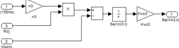
B. Third-Harmonic Output Voltage Control
The third-harmonic frequency control loop is responsible to maintain the dc bus voltage of the DPFC converter by using the third-harmonic frequency power. As the line current contains two frequencies components, the third harmonic current through the line is selected as reference to inject a controllable voltage vector in series with the line, absorbing or generating active power from the transmission line.
For this purpose, the injected voltage should emulate a slow time varying series resistor R(t) such that the transformer should see a secondary winding voltage vo3:
3 3. ( ).3
o h
v =n R t i (21)
where i3h is the line current at fundamental frequency and
n3 the transformer winding ratio. The exchanged energy between DPFC and the transmission line varies in response to the change of the virtual resistance R(t). As a result, the dc bus voltage can be controlled. In the proposed controller, R(t) is controlled with a simple proportional-integral (PI) controller applied to the error between reference dc bus voltage Udcref and actual dc bus voltage Udc=Uc1+Uc2, as following:
0 ( ) ( ) p T( ) p dcref dc dcref dc i K R t K U U U U dt T = − +
∫
− (22)where Kp is the proportional gain and Ti is the integral time of the controller. Fig. 9 represents the virtual resistance control block diagram.
Figure 9 – Virtual resistance R(t) block diagram
To obtain the output voltage vector vo3, the correspondent leg of the converter (γ3) is controlled to generate a PWM output voltage vPWM so that its mean value, in each switching period TPWM, equals the desired
section A, the sliding surface that determines the semiconductors switching law can be written as:
3 3 0 3 ( , ) PWM( ) 0 o o T v v o PWM S e t =K
∫
v −v dt= (23)Fig. 10 represents the sliding surface block diagram of the third-harmonic output voltage controller.
Figure 10 – Block diagram of the vo3 voltage sliding surface As for the fundamental output voltage controller, from the sliding surface (23) one can obtain the correspondent switching law and the single-phase half-bridge PWM modulator that provides the switching variable γ3. The switching signals S31 and S32 applied to the semiconductors are obtained from the switching variable γ3.
C. Capacitor Voltages Equalization
In the DPFC converter topology presented in Fig. 5 it is essential to balance the capacitor voltages Uc1 and
Uc2, to ensure an approximately Udc/2 neutral point voltage. The capacitor voltages equalization technique is a level selection method for the vo2 output voltage in order to control the L2 inductance current (i2), allowing the exchange of active power between the two capacitors.
Uc1 and Uc2 voltage balance is given by:
1 2 0
Uc
e =Uc Uc− = (24)
To ensure condition (24), using sliding mode control method, the sliding surface (25) is defined.
1 2
( Uc, ) Uc Uc. Uc( C C ) 0
S e t =k e =k U −U = (25)
Considering identical capacitors (C=C1=C2) in the DPFC converter topology presented in Fig. 5, the capacitor voltage differential equation (9) can be rewritten as: 1 2 3 1 2
(
) i i i
d Uc Uc
dt
C
+ +
−
=
(26)where i2 is the current to be controlled and i1+i3 are control disturbances.
Assuming a small error ε for the sliding surface (25) and considering the capacitor voltage differential equation (26), the switching law is:
2 2 2 2 ( , ) ( , ) 0 0 ( , ) ( , ) 0 0 Uc Uc Uc Uc di S e t S e t i dt di S e t S e t i dt ε ε > + ⇒ < ⇒ ↓⇒ < < − ⇒ > ⇒ ↑⇒ > (27)
Considering the converter output current equation (10), where: 2 2 2 o
di
v
L
dt
= −
(28)the switching law (27) can be rewritten as:
2 2 2 2 2 2 ( , ) 0 1 2 ( , ) 0 0 2 dc Uc o o dc Uc o o U S e t v v U S e t v v ε γ ε γ > + ⇒ > ⇒ = ⇒ = < − ⇒ < ⇒ = − ⇒ = (29)
Switching law (29) provides the switching variable
γ2 from which it obtains the switching signals S21 and S22 applied to the semiconductors.
IV. SIMULATION RESULTS
In this section simulation results are presented in order to show the power flow control capability of the designed controller.
For the proposed controller, switching models were built in Matlab/Simulink environment and simulations were carried considering the implementation of the DPFC in a medium voltage network. All simulations parameters are presented in Table 3.
The simulation considers a transmission line with a total of 4500 DPFC devices (1500 devices per line) with an 0.1pu power flow control capability, which means that each DPFC device must handle SDPFC=6,75KVA. To guarantee a low harmonic distortion of the transmission line current, the injected third-harmonic current should not exceed 10% of the line nominal current, so I3h=74A.
Fig 11 shows the sinusoidal waveforms of the third-harmonic output voltage (vo3) and its reference (vo3ref).
Figure 11 – Third-harmonic converter output voltage
0.2 0.21 0.22 0.23 0.24 0.25 0.26 0.27 0.28 0.29 0.30.3 -800 -600 -400 -200 0 200 400 600 800 1000 t (s) V o3, V o3r ef (V ) Vo3 Vo3ref
This injected voltage is responsible to regulate the dc bus voltage by exchanging active power with the line at third-harmonic frequency. The reference output voltage varies in response to the change of the virtual resistance R(t), proportional to the error between the reference dc bus voltage Udcref and the actual dc bus voltage
Udc=Uc1+Uc2.
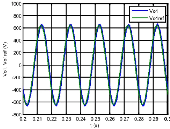
Fig 12 shows the sinusoidal waveforms of the fundamental output voltage (vo1) injected by the converter and its reference (vo1ref). As explained in section III, this capability of injecting a controllable voltage vector allows independent control of the active and reactive power flow. The reference output voltage is calculated according to the specified levels of active and reactive power. As can be seen, the output voltage follows its reference.
Figure 12 – Fundamental converter output voltage
Fig. 13 shows the simulation results of the active and reactive power injected by the converter. As can be seen the controller ensures the power tracking (PDPFC=3,38KW and QDPFC=5,85KVAr). The total power injected by the converter is SDPFC=6,75KVA.
Figure 13 – Active, and reactive power injection
Fig. 14 shows the capacitor voltages Uc1 and Uc2.
Figure 14 – C1 and C2 capacitor voltages
As can be seen the capacitor voltages are balanced, proving the capacitor voltages equalizing strategy capability. Fig. 14 shows both voltages stabilized at the reference dc voltage Ucref=806V.
V. CONCLUSIONS
This paper presented a method and a controller for a distributed power flow controller able to control active and reactive power flow through transmission lines. The DPFC controls the power flow by injecting a controllable voltage vector in series with the line at fundamental frequency. The required active power to maintain the converter dc bus voltage is transmitted through the line at third-harmonic frequency. The DPFC has the same control capability as the UPFC with high reliability because of the redundancy of the multiple series converters. The costs of the DPFC system can be lower than the UPFC because low component rating of the series converter but mainly to series production.
For the proposed converter the switching state-space models were obtained and the control laws of the alternating output voltages were studied using the sliding mode control method. The converter switching laws were defined so that a vector controller of the ac voltages of the converter were obtained.
The performance of the capacitors voltage equalizing strategy was also demonstrated, ensuring that the Uc1 and Uc2 capacitor voltages are balanced and active and reactive power thought the line are controlled.
VI. APPENDIX Table 3 – Simulation parameters
Par. Value Description
Vn 220 KV Transmission line nominal voltage
fn 50 Hz Network natural frequency
Rline 5,2756 Ω Line resistance
Lline 0,0927 H Line inductance
Cline 5,8x10⁻⁷ F Line electrostatic capacitance
Pload 100 MW Load active power
0.2 0.21 0.22 0.23 0.24 0.25 0.26 0.27 0.28 0.29 0.30.3 -800 -600 -400 -200 0 200 400 600 800 1000 t (s) V o1, V o1r ef (V ) Vo1 Vo1ref 0.2 0.25 0.3 0.35 0.4 2000 3000 4000 5000 6000 7000 8000 t (s) P (W ), Q (V ar), S (V A ) P Q S 0.2 0.22 0.24 0.26 0.28 0.3 0.32 0.34 0.36 0.38 0.4 600 700 800 900 1000 Uc 1 ( V ) 0.2 0.22 0.24 0.26 0.28 0.3 0.32 0.34 0.36 0.38 0.4 600 700 800 900 1000 t (s) Uc 2 ( V )
Qload 16,6 MVAr Load reactive power
I3h 74 A Third-harmonic line current
n1 5 Series transformer coupling factor 1
n2 50 Series transformer coupling factor 2
C1 9,8x10⁻³ F Converter C1 capacitor
C2 9,8x10⁻³ F Converter C2 capacitor
L3 3,3 x10⁻³ H Converter L3 inductance
Ucref 806 V Capacitor reference voltage
EUc 8 Admissible error for C1 - C2 voltage
EVo 1 V Admissible error for output voltages
SDPFC 6,75 KVA DPFC power flow control
PDPFC 3,38 KW DPFC reference active power
QDPFC 5,85 KVAr DPFC reference reactive power
REFERENCES
[1] Narain G. Hingorani and Laszlo Gyugyi, Understanding FACTS: Concepts and Technology of Flexible AC Transmission Systems, IEEE Press, 1999.
[2] B. M. Zhang and Q. F. Ding, “The Development of FACTS and its Control”, Proceedings of the 4th International Conference on Advances in Power System Control, Operation and Management, APSCOM-97, Hong Kong, November 1997. [3] K. Sedraoui, K. Al-haddad and G. Olivier, “A
New Approach for the Dynamic Control of Unified Power Flow Controller”, IEEE Power Engineering Society Summer Meeting, 2001. [4] L. Gyugyi, C. D. Schauder, S. L. Williams, T. R.
Rietman, D. R. Torgerson and A. Edris, “The Unified Power Flow Controller: A New Approach to Power Transmision Control”, IEEE Transactions on Power Delivery, 1995.
[5] Deepak Divan and Harjeet Johal, “Distributed FACTS – A New Concept for Realizing Grid Power Flow Control”, Power Electronics Specialists Conference, 36th Annual IEEE[C],
Recife Brazil, 2005.
[6] Deepak Divan, “Improving Power Line Utilization and Performance With D-Facts Devices”, Power Engineering Society General Meeting, IEEE, 2005.
[7] Deepak M. Divan, William E. Brumsickle, Robert S. Schneider, Bill Kranz, Randal W. Gascoigne, Dale T. Bradshaw, Michael R. Ingram and Ian S. Grant, “A Distributed Static Series Compensator System for Realizing Active Power Flow Control on Existing Power Lines”, IEEE Transactions on Power Delivery, vol. 22, nº. 1, January 2007. [8] Harjeet Johal and Deepak Divan, “Design
Considerations for Series Connected Distributed FACTS Converters”, IEEE Transactions on Industry Applications, vol. 43, n.º 6, November 2007.
[9] Zhirui Yuan, Sjoerd W.H. de Haan and Braham Ferreira, “A New FACTS Component – Distributed Power Flow Controller (DPFC)”, European Conference on Power Electronics and Applications, September 2007.
[10] F. Silva and S. Pinto, “Control Methods for Switching Power Converters”, Chapter 34, in
Power Electronics Handbook, 2nd edition, M.H.