Mestrado em Robótica e Automação
AMORPHOUS SILICON 3D SENSORS
APPLIED TO OBJECT DETECTION
Dissertação para obtenção do Grau de Doutor em
Engenharia dos Materiais, especialidade Microelectrónica e Optoelectrónica
Orientador: Doutora Isabel Maria Mercês Ferreira, Professora
Associada, Faculdade de Ciências e Tecnologia da
Universidade Nova de Lisboa
Co-orientador: Doutor Rodrigo Ferrão de Paiva Martins, Professor
Catedrático, Faculdade de Ciências e Tecnologia da
Universidade Nova de Lisboa
Doutor Luis Filipe dos Santos Gomes, Professor
Associado, Faculdade de Ciências e Tecnologia da
Universidade Nova de Lisboa
Júri:
Presidente: Prof. Doutor Paulo da Costa Luís da Fonseca Pinto Arguentes: Prof. Doutor João Lemos Pinto
Prof. Doutor Armando Jorge Miranda de Sousa Vogais: Prof. Doutora Elvira Maria Correia Fortunato
Prof. Doutor Henrique Leonel Gomes Prof. Doutora Maria Teresa Varanda Cidade Prof. Doutor Luís Miguel Tavares Fernandes
i
Mestrado em Robótica e Automação
AMORPHOUS SILICON 3D SENSORS
APPLIED TO OBJECT DETECTION
Dissertação para obtenção do Grau de Doutor em
Engenharia dos Materiais, especialidade Microelectrónica e Optoelectrónica
Orientador: Doutora Isabel Maria Mercês Ferreira, Professora
Associada, Faculdade de Ciências e Tecnologia da
Universidade Nova de Lisboa
Co-orientador: Doutor Rodrigo Ferrão de Paiva Martins, Professor
Catedrático, Faculdade de Ciências e Tecnologia da
Universidade Nova de Lisboa
Doutor Luis Filipe dos Santos Gomes, Professor
Associado, Faculdade de Ciências e Tecnologia da
Universidade Nova de Lisboa
Júri:
Presidente: Prof. Doutor Paulo da Costa Luís da Fonseca Pinto Arguentes: Prof. Doutor João Lemos Pinto
Prof. Doutor Armando Jorge Miranda de Sousa Vogais: Prof. Doutora Elvira Maria Correia Fortunato
Prof. Doutor Henrique Leonel Gomes Prof. Doutora Maria Teresa Varanda Cidade Prof. Doutor Luís Miguel Tavares Fernandes
iii
AMORPHOUS SILICON 3D SENSORS APPLIED TO OBJECT DETECTION
Copyright: Javier Contreras Aparicio FCT/UNL e UNL
A Faculdade de Ciências e Tecnologia e a Universidade Nova de Lisboa têm o direito, perpétuo e sem limites geográficos, de arquivar e publicar esta dissertação através de exemplares impressos reproduzidos em papel ou de forma digital, ou por qualquer outro meio conhecido ou que venha a ser inventado, e de a divulgar através de repositórios científicos e de admitir a sua cópia e distribuição com objectivos educacionais de investigação, não comerciais, desde que seja dado crédito ao autor e editor.
v
In memory of my godfather, Ramon Cañas Represa for setting an example on perfection and of my uncle Pepe Contreras for his successful career and of my friend Ricardo Mengibar for his friendship, during their lifetime.
vii
Acknowledgements
I would like to take this opportunity to thank everyone who supported me and who contributed in some way during my PHD studies.
To my co-supervisor Professor Doctor Rodrigo Martins, my supervisor Professor Doctor Isabel Ferreira and my co-supervisor Professor Luis Gomes for giving me the chance to be able to perform my PHD studies in Portugal, giving me all the necessary support, and funding, so as to complete this project in a satisfactory manner. Most importantly, I would like to thank them for believing in me and my ideas as well as for the fact of giving me the freedom to operate and risk on the scientific initiatives taken. This has given me the necessary knowledge to grow in my career and acquire huge expertise in this area of application.
I would also like to greatly express my gratitude towards Professor Doctor Rodrigo Martins, Professor Doctor Isabel Ferreira and Professor Doctor Elvira Fortunato for their overall help and support during my stay in Portugal and especially for the fact of having to put up with me!
I would like also to thank Professor Luis Gomes and Duarte Guerreiro for providing me with great assistance in order to develop, test, fix, mount, and assemble all electronics systems I have constructed during my stay at CENIMAT-CEMOP, and again, thanks to Professor Luis Gomes for guiding me on the development of electronics and software aspects.
I also specially thank the ASSEMIC European project network and the coordinator in charge Professor Werner Brenner for their cooperation and collaboration for my PhD studies in Portugal.
I would also like to thank Engineer Stephen Thomas from RAL in UK, for helping me enormously during my stay in Portugal with every aspect of his expertise on microelectronics as well as for providing me with some electronic items at no cost whatsoever in order to support my PhD research work. I extend this gratitude towards Mike Homer from SENSTECH in UK, for his help provided on every aspect regarding XDAS system integration as well as for providing me and CENIMAT-CEMOP with faulty X2CHIP components for testing and integration at no cost whatsoever. This appreciation also applies to everyone at RAL and SENSTECH in UK, who has helped me at one point or another.
This expression of gratitude is of course extended to all the partner institutions, staff and fellows from the ASSEMIC European project who collaborated with me and CENIMAT-CEMOP in secondments, meetings and conferences. This allowed the proposed objectives to be reached successfully. I thank specially, Marek Idzikoski from the University of Oldenburg, for providing me that extra help that an expert programmer like him is able to deliver. And I also thank Rafal Wierzibicki for providing me with micro objects for my experiments and Samuel Serra from RAL in UK for providing assistance with CENIMAT-CEMOP’s developments. Of course this thankfulness
viii
also applies to the staff and fellows inside my own institution, namely being CENIMAT-CEMOP. Therefore I thank David Alves (now at INETI), Daniel Costa, Miguel Moreira, Ricardo Ferreira and Carlos Alcobia for helping me with the electronics testing and development and for the discussions held.
I thank Leonardo Silva for his help and discussions held during my stay at CENIMAT-CEMOP as well as for the efforts made.
I specially thank Sonia Pereira, Lucia Gomes, Diana Gaspar, Antonio Vicente, Tiago Mateus, Sergej Filonovich and Professor Doctor Hugo Águas, from CENIMAT-CEMOP for their valuable help regarding the fabrication of 3D sensors.
I specially thank Sergej Filonovich and Professor Doctor Hugo Águas for their extra help, advices and discussions regarding the 1D-3D sensors during my stay at CENIMAT-CEMOP.
I specially thank Pawel Wojcik and Antonio Vicente for their help and discussions on experiments and manuscript image preparation. I thank Ricardo Ferreira for his general help on various technical aspects.
Of course, also I can’t forget the help given by the rest of my colleagues at CENIMAT-CEMOP, such as Luis Pereira, Alexandra Gonçalves, Gonzalo Gonçalves, Pedro Barquinha, Iwona Bernacka, Manuel Quintela, Carla Saldanha, Filomena Calixto, Sara Oliveira, Joana Vaz Pinto, Raquel Barros, Vitor Figueiredo, Paulo Manteigas, Rita Branquinho, Sonia Seixas and Salomão Lopes, amongst others. I also thank anyone who helped me along these years and whom I have forgotten to mention here.
I would also like to thank FCT-MCTES for providing me with the PhD fellowship SFRH/BD/62217/2009.
Finally, I would like to thank my family for supporting me during my PhD studies and stay in Portugal.
ix
Resumo
Hoje em dia, as câmaras 3D e microscópios disponíveis no mercado usam sensores digitais ou discretos, como por exemplo CCDs ou CMOS para aplicações de deteção de objetos. No entanto, estes sistemas não são suficientemente rápidos para algumas aplicações porque precisam de grandes recursos no processamento da informação e podem ser lentos. Portanto, existe um claro interesse na exploração das possibilidades de aplicação de sensores analógicos tal como os arrays de sensores de posição, com o objetivo final de integrá-los em câmaras de varrimento 3D ou na deteção de micro objetos.
O trabalho realizado nesta tese pretendeu contribuir com um estudo detalhado para a implementação de protótipos de sistemas de deteção de objetos utilizando sensores de posição (PSD) de 32 e 128 linhas que foram fabricados na câmara limpa do CENIMAT-CEMOP. Durante a primeira fase do trabalho, o ponto de partida consistiu na fabricação e no estudo das especificações estáticas e dinâmicas dos sensores e seu condicionamento em relação ao conhecimento científico e tecnológico existente. Consequentemente, foi implementada a eletrónica adequada e relevante para a aquisição de dados e processamento de sinais. Vários protótipos foram construídos com arrays de sensores PSD de 32 e 128 linhas. Soluções óticas apropriadas foram integradas para funcionar com os protótipos construídos, permitindo realizar os testes necessários à obtenção dos resultados apresentados nesta tese. O software de controlo, aquisição de dados e plataforma de varrimento 3D foram implementados e combinados para formar vários sistemas integrados com os sensores 3D (arrays de PSDs) de 32 e 128 linhas. O rendimento do array de sensores PSD de 32 linhas e respetivo sistema de aquisição foi testado em aplicações de visão de máquina, como por exemplo o varrimento de objetos em 3D, e também para aplicações de microscopia, com por exemplo a deteção de movimento de micro objetos. Também foram realizados testes em arrays de sensores PSD de 128 linhas tendo-se obtido não linearidades de aproximadamente 4 a 7% nos sensores 1D. Os resultados obtidos mostram a possibilidade de usar um array linear de 32/128 sensores 1D baseados na tecnologia do silício amorfo para o varrimento de objetos 3D e replicação do seu perfil. O sistema e a configuração da plataforma 3D apresentada permite o varrimento 3D a elevadas velocidades e taxas de aquisição. O detalhe ou defeito mínimo que pode ser detetado pelo sistema e sensor é de aproximadamente 350μm usando a configuração estudada. Também é possível identificar as dimensões reais de um objeto 3D em função do ângulo de varrimento, na gama de 15º a 85º, da distância objeto-sensor e da ótica utilizada. Usando estes sensores e respetivo sistema de deteção, objetos simples e complexos podem ser reproduzidos em 3D com elevada precisão e resolução. O sistema de sensores de estrutura nip pode detetar objetos com cores primárias e mesmo com cores derivadas, pelo ajuste correto do tempo de integração do sistema e pela combinação de fontes de luz branca e vermelha, verde e azul (RGB), tendo-se obtido um erro colorimétrico médio de 25,7. Para além disso, o sistema produzido também permite detetar o movimento de micro objetos com recurso a um microscópio. Este oferece a possibilidade de detetar se
x
um micro objeto está em movimento, as suas dimensões (2D) e a sua posição, mesmo para elevadas velocidades de varrimento. Os resultados mostram uma não-linearidade de cerca de 3% e uma resolução < 2µm.
Palavras-chave: Silício amorfo, sensores de posição, deteção de objetos 3D, triangulação laser, deteção de movimento de micro objetos
xi
Abstract
Nowadays, existing 3D scanning cameras and microscopes in the market use digital or discrete sensors, such as CCDs or CMOS for object detection applications. However, these combined systems are not fast enough for some application scenarios since they require large data processing resources and can be cumbersome. Thereby, there is a clear interest in exploring the possibilities and performances of analogue sensors such as arrays of position sensitive detectors with the final goal of integrating them in 3D scanning cameras or microscopes for object detection purposes.
The work performed in this thesis deals with the implementation of prototype systems in order to explore the application of object detection using amorphous silicon position sensors of 32 and 128 lines which were produced in the clean room at CENIMAT-CEMOP. During the first phase of this work, the fabrication and the study of the static and dynamic specifications of the sensors as well as their conditioning in relation to the existing scientific and technological knowledge became a starting point. Subsequently, relevant data acquisition and suitable signal processing electronics were assembled. Various prototypes were developed for the 32 and 128 array PSD sensors. Appropriate optical solutions were integrated to work together with the constructed prototypes, allowing the required experiments to be carried out and allowing the achievement of the results presented in this thesis. All control, data acquisition and 3D rendering platform software was implemented for the existing systems. All these components were combined together to form several integrated systems for the 32 and 128 line PSD 3D sensors. The performance of the 32 PSD array sensor and system was evaluated for machine vision applications such as for example 3D object rendering as well as for microscopy applications such as for example micro object movement detection. Trials were also performed involving the 128 array PSD sensor systems. Sensor channel non-linearities of approximately 4 to 7% were obtained. Overall results obtained show the possibility of using a linear array of 32/128 1D line sensors based on the amorphous silicon technology to render 3D profiles of objects. The system and setup presented allows 3D rendering at high speeds and at high frame rates. The minimum detail or gap that can be detected by the sensor system is approximately 350 μm when using this current setup. It is also possible to render an object in 3D within a scanning angle range of 15º to 85º and identify its real height as a function of the scanning angle and the image displacement distance on the sensor. Simple and not so simple objects, such as a rubber and a plastic fork, can be rendered in 3D properly and accurately also at high resolution, using this sensor and system platform. The nip structure sensor system can detect primary and even derived colors of objects by a proper adjustment of the integration time of the system and by combining white, red, green and blue (RGB) light sources. A mean colorimetric error of 25.7 was obtained. It is also possible to detect the movement of micrometer objects using the 32 PSD sensor system. This kind of setup offers the possibility to detect if a micro object is moving, what are its dimensions and what is its position in
xii
two dimensions, even at high speeds. Results show a non-linearity of about 3% and a spatial resolution of < 2µm.
Keywords: Amorphous silicon, position sensitive detectors, sheet-of-light range imaging, micro object detection, triangulation systems, 3D object detection
xiii
Table of contents
Chapter 1. Machine Vision... 3
Summary ... 3
1.1. Introduction ... 3
1.2. Components of a machine vision system ... 5
1.3. Photodiodes ... 6
1.3.1. Operating characteristics of a photodiode ... 6
1.4. Discrete image sensors ... 11
1.4.1. Charged Coupled Devices (CCDs) ... 11
1.4.2. Complementary Metal Oxide Semiconductor (CMOS) Imagers ... 13
1.4.3. Comparison table CCD versus CMOS ... 15
1.5. Analogue sensors ... 16
1.5.1. Position Sensitive Detectors (PSDs) ... 16
1.5.2. One dimensional PSD ... 16
1.5.3. Two dimensional PSD ... 18
1.5.4. Three dimensional PSD ... 19
1.5.5. Amorphous silicon PSDs ... 20
1.5.6. Amorphous silicon versus Crystalline silicon ... 21
1.6. Optics ... 22
1.6.1. Reflection ... 22
1.7. Light sources ... 23
1.8. Colour ... 24
1.8.1. RGB or additive colour ... 24
1.8.2. CMYK subtractive colour ... 25
1.8.3. Colour models ... 26
1.8.4. Human colour vision ... 27
1.8.5. Colour sensors ... 28
1.9. 3D PSD for micro objects ... 29
1.10. References ... 31
Chapter 2. Applications of machine vision ... 37
Summary ... 37
2.1. Machine vision techniques ... 37
2.1.1. Stereovision ... 38
2.1.2. Continuous wave modulation ... 38
2.1.3. Time-of-flight ... 39
2.1.4. Light triangulation ... 39
2.2. Machine vision state of the art ... 43
2.2.1. Traditional contact commercial systems ... 43
xiv
2.3. Discrete sensor based machine vision applications ... 49
2.4. Analogue sensor based machine vision applications ... 50
2.5. Conclusions on machine vision ... 51
2.6. Microscopy applications ... 52
2.6.1. Discrete sensor based microscopy applications ... 52
2.6.2. Analogue sensor based microscopy applications ... 53
2.6.3. Fluorescence approaches ... 53
2.6.4. Tracking ... 54
2.6.5. Conclusions on microscopy ... 55
2.7. References ... 56
Chapter 3. Experimental procedures ... 61
Summary ... 61
3.1. Fabrication of a-Si:H 32/128 position sensitive detector arrays ... 61
3.1.1. Cleaning of the substrate ... 62
3.1.2. Photolitography ... 62
3.1.3. Metallization ... 63
3.1.4. Lift-off ... 64
3.1.5. PECVD – Plasma Enhanced Chemical Vapour Deposition ... 64
3.1.6. Dry etching ... 65
3.1.7. Sputtering ... 65
3.1.8. Wet etching ... 66
3.2. Hardware development for PSD sensor array systems ... 67
3.2.1. 32 PSD sensor array hardware system ... 67
3.2.2. 128 PSD sensor array hardware system ... 69
3.3. Software development for PSD sensor array systems ... 72
3.3.1. 128 PSD sensor array software platform ... 74
3.4. Machine vision ... 74
3.4.1. Dynamic experimental procedure ... 75
3.4.2. Static experimental procedure ... 76
3.4.3. 3D object profiling experimental procedure ... 77
3.5. Detection of micro objects ... 77
3.5.1. Sensor/System micropositioning experimental procedure ... 78
3.6. Sensor spectral response experimental procedure ... 82
3.7. References ... 82
Chapter 4. Results and discussions ... 85
Summary ... 85
4.1. Dynamic response ... 85
4.2. Static response ... 88
xv
4.4. Sensor degradation ... 95
4.5. Dynamic response to different colour illumination ... 97
4.5.1. Dynamic response with red and green laser ... 98
4.6. Dynamic response to colour objects ... 99
4.7. 3D Scanning characteristics of the sensor/system ... 100
4.7.1. 3D profile detection setup ... 101
4.7.2. 3D profile detection resolution ... 104
4.7.3. Influence of the incident angle on the detection resolution ... 107
4.7.4. Geometry analysis of the triangulation platform ... 109
4.7.5. Resolution and accuracy ... 115
4.7.6. Repeatability of measurements ... 117
4.7.7. 128 PSD array system 3D object profile scanning ... 118
4.8. 3D object profiling results ... 120
4.8.1. Low resolution 3D object scanning ... 120
4.8.2. High resolution 3D object scanning... 121
4.9. Colour sensing ability of the sensor/system ... 124
4.9.1. Static colour detection response ... 130
4.9.2. Dynamic colour detection response ... 132
4.10. Microscopy applications ... 139
4.10.1. Raw sensor micropositioning results ... 140
4.10.2. Sensor/System micropositioning results ... 144
4.10.3. Sensor/System microgripper detection results ... 150
4.11. References ... 156
Chapter 5. Final conclusions and future work ... 161
Summary ... 161
5.1. Conclusions regarding the use of the sensor/system for machine vision ... 161
5.2. Conclusions regarding the use of the sensor/system for microscopy ... 163
5.3. Future work ... 164
APPENDIX A - Fabrication of the amorphous silicon position sensitive detector arrays
(PSD arrays) ... 167
APPENDIX B - Hardware and software developments for the amorphous silicon
position sensitive detector array (PSD array) systems ... 181
xvii
List of Figures
Figure 1.1 – European market total turnover of vision products 2006. Percentage turnover shares by
industries (%) [5]. ... 4
Figure 1.2 – Worldwide total turnover of Vision Products 2006 by regions (%) [5]. ... 5
Figure 1.3 – Equivalent circuit of a silicon photodiode [7]. ... 7
Figure 1.4 – Photodiode response waveform [7]. ... 8
Figure 1.5 – Trans-impedance amplifier read out circuitry of photodiode [9]. ... 9
Figure 1.6 – Photo-current/Voltage curves under different level of illumination [7]. ... 10
Figure 1.7 – Schematic of the architecture of a CCD (Interline type) [14]. ... 12
Figure 1.8 – (a) Photograph of an “Area Scan” or large pixel area CCD (b) Photograph of a “Line Scan” or linear array of pixels CCD, (c) Photograph of a TDI (Time Delay and Integration) “Line Scan” CCD manufactured by DALSA Corporation [16]... 13
Figure 1.9 – (a) Schematic of the architecture of a CMOS Imager [14]; (b) Photograph of a CMOS imager manufactured by DALSA Corporation [16]. ... 14
Figure 1.10 – Principle of operation of a 1D PSD. ... 17
Figure 1.11 – Sketch of a 1-Dimensional PSD [21]... 17
Figure 1.12 – Sketch of a duo-lateral 2-Dimensional PSD [21]. ... 18
Figure 1.13 – Sketch of the typical shape measurement triangulation application example [adapted from 6]. ... 19
Figure 1.14 – Photograph of the 128 element PSD linear array manufactured by Hamamatsu [6]. ... 20
Figure 1.15 – Photograph of the 128 element PSD linear array developed at CEMOP/UNINOVA. ... 20
Figure 1.16 – Examples of the different types of reflectance [40]. ... 22
Figure 1.17 – Red, green and blue (RGB) or additive colour scheme. ... 25
Figure 1.18 – Internal geometry of the Munsell colour system and CIELUV colour space [43]. ... 26
Figure 1.19 – (a) Spectral response of the three colour detection cones inside the human eye [44] (b) Overall sensitivity of the human eye [45]. ... 28
Figure 1.20 – Optical path followed by light inside a microscope. ... 30
xviii
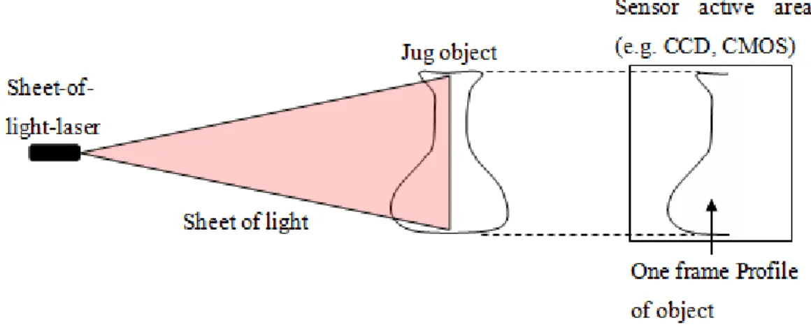
Figure 2.2 – Schematic of the sheet-of-light 3D scanning of a jug and one frame projected on sensor
... 41
Figure 2.3 – Sheet-of-light commercial range scanner manufactured by Integrated Vision Products [adapted from 4]. ... 42
Figure 2.4 – Example of occlusions in sheet-of-light systems. ... 43
Figure 3.1 – Photographs of the masks for: a) metal; b) silicon; c) TCO layers ... 63
Figure 3.2 – Photograph of the sputtering system. ... 65
Figure 3.3 – Photograph of the 32 position sensitive detector (PSD) array sensor. ... 66
Figure 3.4 – Photograph of the data acquisition prototype system. ... 67
Figure 3.5 – Schematic of the main electronics system module responsible for the data acquisition and control [5]. ... 68
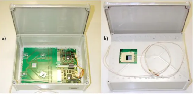
Figure 3.6 – a) View of the XDAS 128 sensor system. b) View of the 128 sensor socket exposed outside the box for light detection purposes. ... 70
Figure 3.7 – XDAS System for 128 PSD data acquisition. ... 70
Figure 3.8 – NIDAQ 128 system. Circuit board ready for testing in conjunction with 128 PSD sensor. ... 71
Figure 3.9 – (a) 3D representation of the white plastic fork on the 3D map. (b) Plastic white fork scanned using a RED laser line. ... 73
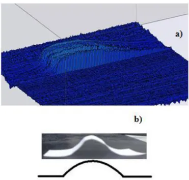
Figure 3.10 – (a) 3D object profile of the blank sheet of paper shaped to form a small bump. (b) Blank sheet of paper shaped to form a small bump. ... 74
Figure 3.11 – Sketch of the generic experimental setup composed of a laser line source, an optical lens, a white plastic ramp, a translation table, and the system integrating a 32 PSD array sensor. . 75
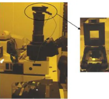
Figure 3.12 – Photograph of the microscope system used with the sensor holder in detail. ... 78
Figure 3.13 – (a) Sketch of the 32 linear array of 1D detectors including the image of the cantilever and its corresponding starting movement position. (b) Photograph of the PSD. (c) Photographs of the object (cantilever and its holding structure supplied by NASCATEC GmbH. ... 79
Figure 3.14 – Photograph of the experimental setup including the built data acquisition prototype, the microscope and the micro cantilever or microgripper together with its holding structure. ... 80
Figure 3.15 – Sketch of the light path, sensor, microgripper and reflected image setup ... 81
Figure 4.1 – Dynamic response and linearity of sensor channel 14 and 11 at integration times of 1ms and 0.5 respectively. Distance scanned vs. position on the sensor. ... 85
xix
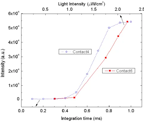
Figure 4.2 – Dynamic response at integration times of 1ms, 0.8ms, 0,7ms, 0.6ms and 0.5ms respectively. Distance scanned versus position on the sensor. ... 87 Figure 4.3 – Dynamic response and linearity of sensor channel 26 at an integration time of 0.6ms together with the same response acquired under sub-sampling conditions. Distance scanned versus position on the sensor. ... 88 Figure 4.4 – Static responses of sensor contacts 4 and 6. Intensity (in arbitrary units) of the sensor as a function of the integration time (or system amplification), and corresponding light intensity. .... 89 Figure 4.5 – Static responses of sensor contact 56. Signal intensity (in arbitrary units) as a function of light intensity and integration time. ... 90 Figure 4.6 – Relationship between filtered light intensity and system integration time for sensor contacts 6, 18, 30, 54 and 56. ... 91 Figure 4.7 – Dynamic response of channel 22 at an integration time of 0.6ms and 128 subsampling
for a small bump glued on the ramp. The photograph of the bump is displayed inside the figure. . 92 Figure 4.8 – Photograph of the small white plastic bump cut into 4 parts. These parts were separated by the gaps shown. ... 93 Figure 4.9 – Dynamic response of 3 channels at 0.32mm/sec, 0.6ms integration time for a small bump cut in 4 parts and glued on the ramp. ... 93 Figure 4.10 – Dynamic response of 5 channels at 9.6mm/sec, 0.6ms integration time for a small bump cut in 4 parts and glued on the ramp. ... 94 Figure 4.11 – Experimental setup for studying the degradation of the 32 PSD sensor ... 95 Figure 4.12 – Variation of the sensor channel signal intensity over time (170 hours), while being exposed to light. ... 96 Figure 4.13 – Comparison of the degradation percentage range for sensors without SiO2, 2-11 (blue),
and with SiO2, 3-11 (red). ... 97
Figure 4.14 – Measured spectral response of a single amorphous silicon PSD element from the sensor array. ... 98 Figure 4.15 – Dynamic response of sensor channel 14 for Red (0.8ms/10pF) and Green (0.5ms/2pF) lasers. ... 99 Figure 4.16 – Dynamic response and linearity of sensor channel 13 at an integration time of 1ms. Distance scanned versus position on the sensor. ... 100 Figure 4.17 – (a) Sketch of the experimental setup for 3D profile scanning. (b) Photograph of the experimental setup. ... 101
xx
Figure 4.18 – (a) Horizontal photograph of the white rubber (object) with black and white pattern glued on top. (b) Black and white pattern (50 µm – 1000 µm). ... 102 Figure 4.19 – Sketch of how the reflection of the height of the object looks like on the sensor active area. This is one frame of the object. (a) Laser line not incident on the object. (b) Laser line strikes the object. (c) Laser line does not strike the object. (d) Laser line strikes the object. (e) Laser line strikes a black stripe on the object (same as no object). (f) Laser line strikes the object. ... 103 Figure 4.20 – (a) Sketch of the 3D scanning response of sensor channel 11 when rendering the white rubber object glued with the black and white pattern. (b) Sketch of the magnification of the smallest peak detected from the 3D scanning response of sensor channel 15 when rendering the white rubber object glued with the black and white pattern. (c) Sketch of the 3D scanning response of sensor channel 17 when rendering the side region indicated, corresponding to the white rubber itself without the black and white pattern. ... 105 Figure 4.21 – Sketch of the 3D scanning response of sensor channel 4 at several angles when rendering the white rubber itself. ... 108 Figure 4.22 – Sketch of the 3D scanning response of sensor channel 17 at several angles when rendering the white ramp. ... 108 Figure 4.23 – Schematic of the geometry of the triangulation platform scheme. ... 110 Figure 4.24 – Sketch of the theoretical versus the experimental values of w for the angles of interest.
... 114 Figure 4.25 – Scan of the white rubber object by channel 12 of the sensor. Acquisition time of 8ms.
... 116 Figure 4.26 – White rubber object 3D profile scans. 20 repeated scans obtained with channel 13 of the sensor. ... 117 Figure 4.27 – (a) Photograph of a white rubber object. (b) 3D object profile representations for the individual detections of channels 54 (128 PSD array sensor A) and 75 (128 PSD array sensor B). ... 119 Figure 4.28 – 3D Image of rendered fork using only 110 frames for the whole scan. The height of the fork is represented by respective sensor position values in the Z-axis. ... 120 Figure 4.29 – (a) High resolution 3D rendered profile of the white colour rubber. (b) High resolution 3D rendered profile of the white colour fork. ... 122 Figure 4.30 – (a) Photograph of the white plastic fork. (b) 3D Object representation of the scanned white plastic fork. ... 123 Figure 4.31 – Experimental setup for the scanning of the attached sample. ... 126
xxi
Figure 4.32 – (a) Schematic view of the reflectivity of the colour surface in accordance to the correspondent light colour being used. RGB incident light was obtained using filters whose transmittance is shown. (b) Red filter, Green filter, Green/Blue filter. (c) Blue filter by combining two different filters. ... 127 Figure 4.33 – Photograph of the combined colour surface attached to the white plastic ramp with the simulated projection of a white light stripe (white mark). (a) Primary RGB colours. (b) Derived/intermediate colours. ... 128 Figure 4.34 – Reflectance over the spectral wavelength range from 300nm to 800nm for the 14 individual target colour surfaces of the combined colour surface (a) Reflectance for the white paper, white plastic and primary colour surfaces. (b) Reflectance for the derived colour surfaces. (c) Reflectance for the intermediate colour surfaces. ... 129 Figure 4.35 – Mirror surface reflection. Power light intensity versus integration time. ... 131 Figure 4.36 – Static surface colour analysis using white, red, green and green/blue light. Power light intensity versus integration time, CH25... 131 Figure 4.37 – Dynamic surface colour analysis using white, red, green and green/blue light. Power light intensity versus distance. Comparison to static surface colour analysis. (a) White light, CH25. (b) Red light, CH26 (c) Green light, CH25 (d) Green/Blue light CH25. ... 133 Figure 4.38 – Normalized relative light intensity as a function of the distance from right to left for the combined colour surface scanned (white, red, green and blue light). ... 135 Figure 4.39 – CIELUV plot. Comparison between detected colours from the sensor system and reference colours measured by the spectrophotometer. ... 137 Figure 4.40 – Photovoltage measured at several 1D detectors of the 32 lines array sensor with and without focusing lens; (a) without image reflected (background) and (b) with image reflected. .. 140 Figure 4.41 – Photovoltage signal measured at different lines of the 32 array PSD sensor and respective sketch of the object image for each corresponding position. ... 141 Figure 4.42 – (a) Photovoltage signal measured at different lines of the 32 array psd sensor and (b) enlargement of the region indicated in (a). ... 142 Figure 4.43 – (a) Response of the active sensor lines at a photovoltage of 100 mV as a function of Y position of the object (holding structure of cantilever). (b) Voltage signal of the top electrode of the sensor as a function of X position for a fixed Y position corresponding to the cantilever detection. ... 143 Figure 4.44 – (a) Sketch of the micro cantilever entering parallel to the sensor lines. It enters approximately at the centre of the sensor at detector 17 or 18 (b) Sketch of results according to
xxii
when no focusing lens is used (c) Sketch of results for when the micro cantilever is immersed inside a liquid. ... 145 Figure 4.45 – Sketch of the micro cantilever moving sideways, after having entered parallel to the sensor lines as in figure 4.44. ... 146 Figure 4.46 – (a) Sketch of the micro cantilever and its holding structure entering perpendicular to the sensor lines (b) Sketch of the response of each detector at the 3 nA threshold level, when just the holding structure of the cantilever is present (c) Sketch of the measured data at each detector for the 3 nA threshold level and its related linear fit. ... 147 Figure 4.47 – (a) Sketch of the micro cantilever moving sideways, after having entered perpendicular to the sensor lines as in figure 4.46. (b) Sketch of the best channel response from figure 4.47(a) and its related calculated linearity. ... 149 Figure 4.48 – Picture of the microgripper and its structure. ... 151 Figure 4.49 – Microgripper in parallel to the 32 PSD sensor active area. ... 152 Figure 4.50 – (a) Picture of the microgripper as seen on the ocular of the microscope. (b) PSD system detection of gripper at 3.5X magnification. (c) PSD system detection of gripper at 13.5X magnification. ... 153 Figure 4.51 – (a) Picture of the microgripper tips. (b) PSD system detection of gripper tips at 3.5X magnification. (c) PSD system detection of gripper tips (3.5X) when closed 15º (63V). ... 153 Figure 4.52 – Microgripper Y-axis movement PSD system detection (13.5X magnification). (a) No gripper. (b) Gripper tips. (c) Middle part of tweezers. (d) Beginning of tweezers. (e) Part of gripper structure and part of tweezers. (f) Gripper structure and small part of tweezers. ... 154 Figure 4.53 – Microgripper X-axis movement PSD system detection (13.5X magnification). (a) Middle part of tweezers (figure 4.52(c)). (b) Left tweezer moved right (-0.185mm). (c) Left tweezer moved further right (-0.336mm). (d) Right tweezer moved left (0.357mm). ... 155
xxiii
List of Tables
Table 1.1 – Comparison table CCD vs CMOS ... 15 Table 1.2 – Light source comparison ... 24 Table 2.1 – Traditional commercially available contact systems [adapted from 4]. ... 44 Table 2.2 – Machine vision non contact commercially available systems [adapted from 4]. ... 46 Table 3.1 – Correspondence of filters with light intensity. ... 77 Table 4.1 – Comparison of detected (0.32mm/sec) versus real dimensions of white plastic bump ... 94 Table 4.2 – Resolution of detection at a speed of 1.97 mms-1 ... 106 Table 4.3 – Theoretical calculated values of w, for a fixed h and varying angle β, ... 113 Table 4.4 – Theoretical calculated values of w, for a fixed h and varying angle β, where f=50mm;
p=675mm; q=54mm and h=11.32mm... 114
Table 4.5 – Ratio between signal intensities obtained from different colour surfaces for each light colour source. ... 134 Table 4.6 – CIELUV L*, u’, v’ and ∆E values for the sensor system and spectrophotometer for all target colour surface reflections. ... 138 Table 4.7 – Dimensions of microgripper ... 151
xxv
List of symbols, acronyms and abbreviations
ASIC Application Specific Integrated Circuit a-Si:H Hydrogenated Amorphous Silicon
CCD Charge Coupled Device
CIE Commission Internationale d'Eclairage (International Commission on Illumination) CMM Coordinate measuring machine
CMOS Complementary Metal Oxide Semiconductor CMYK Cyan, Magenta, Yellow and Black
FPGA Field programmable gate array j.n.d Just noticeable difference LED Light emitting diode NEP Noise equivalent power NIP n-i-p semiconductor structure PCB Printed circuit board
PECVD Plasma enhanced chemical vapor deposition P-N P-type and N-type silicon
PIN p-i-n semiconductor structure PSD Position Sensitive Detector Q.E. Quantum efficiency
RF Radio frequency
RGB Red, Green and Blue
SW Staebler-Wronski
TCO Transparent Conductive Oxide
TDI Time delay and integration technology
UV Ultra-violet
VHF Very high frequency
xxvi
µ Micro
Rλ Responsivity
Ip Photocurrent
P Incident light power
λ Wavelength
h Planck’s constant
c Speed of light in vacuum
q Electron charge
Cj Junction capacitance
Rsh Shunt resistance
Rs Series resistance
Iph Incident light generated photocurrent
Id Forward current through diode
Io Output current
Vo Output voltage
RL Load resistance
σe Linearity error
Sm Standard deviation
1
Chapter 1
3
Chapter 1. Machine Vision
Summary
This chapter provides an introduction to machine vision starting by a brief history and market analysis, and subsequently reviewing more in depth, each of the components of a typical machine vision system, with a special emphasis on the characteristics of the existing types of sensors such as discrete or analogue in accordance to the state of the art. Colour concepts are also addressed in this chapter.
1.1. Introduction
Quality is nowadays a critical factor in industry since it allows companies to be competitive in the market while being able to deliver optimum products to its clients. Companies in Japan became pioneers in manufacturing quality products by the 1970s. By the 1990s, companies in Europe and America were obliged to introduce quality control procedures into their goods and manufacturing processes for competing with Japanese ones. Machine vision has become an essential quality control tool for increasing manufacturing quality.
We could define machine vision as the process of designing, developing and integrating automatic imaging systems to improve manufacturing processes in industry. Automation, mechanical engineering, optics and computer science make up machine vision.
However, another suitable definition for machine vision can be quoted:
“The use of devices for optical, non-contact sensing to automatically receive and interpret an image of a real scene in order to obtain information and/or control machines or processes” [1].
The initial concept of using machine vision for industrial inspection dates back to the 1930s, although it was only after the 1970s that the idea developed further into a system. Then in the 1990s, the concept received special interest due to the advances and progress made in vision systems image and processing technology. This resulted in huge growth of the machine vision industry. Finally, in the 2000s, considerable technology improvements have taken place and the market is still growing and expanding at a fast pace.
However, it must be stated that, the successful design and integration of these systems is still a bottleneck and remains a challenge in several areas, partly due to the lack of skilled labour [2].
The components of a machine vision system do not suffer from fatigue as humans do, and neither do they do mistakes or take decisions which could affect the procedure. In machine vision systems it is necessary to collect and process each individual pixel and construct a relevant image
4
from these. Even though human vision has been regarded as impractical for industrial inspection, up to date no machine vision system is capable of matching human optics on some aspects such as, tolerance to changes in lighting and degradation of the image, interpretation and comprehension of the image, flexibility or variability of parts inspected, etc. On the other hand, some industrial applications do not need the high precision offered by human vision [3, 4]. Tasks typically allocated to these systems include the detection of surface defects, serial number identification, counting parts on a conveyor belt, etc. Amongst the vast majority of sectors, automobile and semiconductor manufacturing, pharmaceutical packing and film container printing are some related examples. So, today, machine vision systems are a vital component of quality control processes present in all areas of industry.
Figure 1.1 illustrates the European vision technology market, total turnover of vision products, in the year 2006. The automotive sector amounts to a great percentage of the manufacturing industry, 29% of the market share, and this is followed by the glass, printing, electronics and other sectors.
Figure 1.1 – European market total turnover of vision products 2006. Percentage turnover shares by industries (%) [5].
Figure 1.2 shows the total revenue derived from vision products worldwide in the year 2006. Europe accounts for 68% of the market share and it is particularly interesting that the highest percentage of sales achieved worldwide by European Companies were in Portugal and Spain [5].
5
Figure 1.2 – Worldwide total turnover of Vision Products 2006 by regions (%) [5].
Traditional machine vision systems usually employ a Charged Coupled Device (CCD) as the vision sensor component. A CCD is normally comprised of a matrix of pixels and so therefore each pixel has to be analysed and processed when an image is projected on it.
In the following work the CCD's detection principle and components are revised in order to be compared to position sensitive detectors (PSD).
1.2. Components of a machine vision system
A typical machine vision system is usually composed of several or all of the following components:
One or more image sensor structures. Usually one or more digital or analogue cameras are used.
Suitable optics for image focusing and projection. Lenses are normally used to focus the desired field of view onto the image sensor.
Suitable light sources (Lasers, LEDs, Fluorescent or Halogen lamps, etc).
An interface device (analogue to digital converter) to digitize and transfer images to the processor/PC.
Input/Output hardware. Usually being a processor/PC or embedded processor. Software platforms for image processing and representation. These platforms are also
currently used to detect and recognise relevant image features.
A synchronized system configuration involving sensors (magnetic, optical, etc) to detect movement of parts, for example, on a production line which would trigger image acquisition and processing. Actuators are also welcome to sort, route or reject defective parts if
6
1.3. Photodiodes
The most used sensor structures in CCDs are silicon PIN photodiodes since they have a fast response speed, an excellent photo to dark current ratio and a wide spectral response. Other existing types of structures are PN, Schottky and Avalanche junctions however they have lower sensitivity performances [6].
1.3.1.
Operating characteristics of a photodiode
1.3.1.1.
Spectral response
The spectral response or responsivity (Rλ) is the ratio of the photocurrent Ip to the incident
light power P at a given wavelength of a silicon photodiode [7].
[1.1]
where, Rλ units are A/W.
1.3.1.2.
Quantum Efficiency
Quantum efficiency, Q.E., is the ratio of the number of charge carriers (or electron-hole pairs) generated to the number of photons striking the detector and it is related to responsivity Rλ by [7]:
[1.2]
where, λ is the wavelength of the light in nanometers (nm), h is Planck’s constant (6.63 × 10 -34
Js), c is the speed of light in vacuum (3 ×10⁸ m/s), and q is the electron charge (1.6 × 10⁻¹⁹ C).
1.3.1.3.
Linearity
As far as sensor detection is concerned, linearity is an important characteristic, as a linear increase of the generated photocurrent in accordance with an increase of the incident light power must be verified. Noises current as well as the series and load resistances determine linearity. Photodiode nonlinearities are typically less than 1%. Figure 1.3, shows a photodiode’s equivalent circuit where an ideal diode is in parallel with a current source, a junction capacitance Cj and a shunt resistance Rsh and
in series with resistance Rs:
P
I
R
p
R
q
hc
R
E
Q
.
.
1240
7
Figure 1.3 – Equivalent circuit of a silicon photodiode [7].
where, Iph is the incident light generated photocurrent, Id is the forward current through the
diode, Io is the output current and Vo is the output voltage.
The p-n junction is represented by the diode and the photocurrent generated by the incident light is represented by the current source. An ideal photodiode should have no series resistance and an infinite shunt resistance [7-9]. Dark current is the existing leakage current flowing when the photodiode is in dark conditions. Extremely low light levels, when the photocurrent equals the level of the noise generated, compromise the usefulness of the device.
1.3.1.4.
Response time
The product of the junction capacitance Cj and the external load resistance RL shown in figure
1.3 determines the response time of a photodiode. In turn, the existing p-n junction depletion region within the photodiode defines the junction capacitance Cj. However, the response time is always
influenced by the load resistance, the wavelength of the light and the applied voltage on the diode. The response time can be analyzed by measuring the rise time tr or the fall time tf. The rise time is the
time taken for the output response to rise from 10% to 90% of its final value and the fall time is the time taken for the output response to fall from 90% to 10% of this same final value. The rise time tr is
defined by the following expression [7]:
[1.3]
where, τ1 is the time constant, determined by the product of the load resistance RL and the
terminal capacitance of the photodiode Ct. Ct is the sum of the photodiode junction capacitance Cj and
the package capacitance.
The rise time tr is also influenced by τ2,which is the diffusion time of carriers generated
outside the depletion layer and when the product of Ct and RL shown in equation 1.3 is small, it is
exclusively τ2 which defines the response time of a photodiode.
L t
R
C
2
.
2
2
.
2
t
r
18
The response waveform of a photodiode is illustrated in the following figure, figure 1.4:
Figure 1.4 – Photodiode response waveform [7].
1.3.1.5.
Operating modes
A photodiode allows the photovoltaic or unbiased mode and the photoconductive or biased operating mode. The specifications of the application determine which operating mode is most appropriate. Photovoltaic mode is suitable for low light level and low frequency applications and it allows simplicity in system design and development. When considering the photoconductive mode of operation, response speed and linearity could certainly improve via the application of a reverse bias, however, dark and noise currents as well as response variations due to temperature are likely to increase.
Despite these drawbacks and as previously stated, for high speed applications such as optical communications and remote control, PIN photodiodes offer not only a good response speed but excellent dark current and voltage resistance characteristics when a reverse voltage is applied.
It is also relevant to know that the measurements of signals from a photodiode can be performed either as a current or voltage. Clearly, a much better performance in terms of linearity, offset and bandwidth is obtained when reading a current, since it is proportional to the incident light power. A trans-impedance configuration should be used in order to convert from current to voltage and in fact the read out circuitry of a photodiode is generally a trans-impedance amplifier as shown below in figure 1.5:
9
Figure 1.5 – Trans-impedance amplifier read out circuitry of photodiode [9].
In order to keep the trans-impedance amplifier stable the impedance Zf is used and this is
usually a resistance Rf in parallel to a capacitance Cf.
1.3.1.6.
Current –Voltage characteristics
The current-voltage curve of an ideal diode shows a small reverse saturation current generated when a reverse bias is applied (VR) and an exponential increase in current occurs for forward bias (VF)
(see figure 1.6). The relationship between the dark and the saturation current of the ideal diode is established by the following equation [7]:
[1.4]
where, ID is the dark current, ISAT is the reverse saturation current, qis the electron charge, VA
is the applied voltage, kB is Boltzmann’s constant (1.38 × 10 -23
J/K) and T is the temperature.
Under illumination and in photovoltaic mode (V = 0) the current given by the diode is the reverse saturation current. Therefore the IV curve in the reverse bias shifted by an amount equal to Ip,
proportional to the level of light power, therefore separate curves are obtained for different light levels which are represented by P0, P1, P2 in figure 1.6. At P1, the photodiode has already been illuminated
and the photocurrent can be obtained by equation 1.5 [7]:
[1.5]
where, ITOTAL is the total current and Ip is the measured photocurrent for a certain light power.
k T1
qV SAT D B Ae
I
I
P T k qV SAT TOTALI
e
I
I
B A
1
10
Figure 1.6 – Photo-current/Voltage curves under different level of illumination [7].
The maximum applied reverse bias voltage can never reach the breakdown voltage, since severe damage can occur on the device, as shown in figure 1.6.
1.3.1.7.
Noise characteristics
In a photodiode the total noise takes into account the Johnson noise and the shot noise. The Johnson noise is related mainly to the shunt resistance, with substantial contribution from all other resistors (including the load resistor) and it is the dominant noise when working in unbiased (photovoltaic) mode. Its magnitude is calculated using the following expression [7]:
[1.6]
where, Ijn is the Johnson noise current, Δf is the noise measurement bandwidth and T is the
temperature.
The shot noise is related to photocurrent and dark current oscillations and it is the dominant noise when working in biased (photoconductive) mode. Its magnitude is calculated using the following expression [7]:
[1.7]
where, Isn is the shot noise current, IP is the photocurrent and Δf is the noise measurement
bandwidth.
The total photodetector noise current is related to the Johnson and the shot noise currents by the following expression [7]:
sh B
R
f
T
k
4
I
jn
I
I
f
q
I
sn
2
P
D
11
[1.8]
where, Itn is the total photodetector noise current, Isn is the shot noise current and Ijn is the
Johnson noise current.
1.3.1.8.
Noise Equivalent Power (NEP)
The quantity of incident light power on a photodiode required to produce a photocurrent equivalent to the existing noise level is regarded as the noise equivalent power and it is given by [7]:
[1.9]
where, NEP is the noise equivalent power (W/(Hz)1/2), Itn is the total photodetector noise
current and Rλ is the responsivity (A/W).
1.4. Discrete image sensors
1.4.1.
Charged Coupled Devices (CCDs)
The use of Charged Coupled Devices or CCDs as image sensors has spread hugely over a broad range of applications ranging from astronomy, medicine or microtechnology to all kinds of recognition and mapping procedures. CCDs are used virtually everywhere, such as for example photographic cameras, standard video cameras, security cameras, fax machines, bar-code readers, photocopiers, and others [10, 11].
The main purpose of a CCD is to generate object images but it is also able to transfer electrical charge or store information. The incident light coming from an object is the optical input to a CCD and the output is an electronic signal which needs to be processed using hardware. Subsequently, suitable software should be used to present the data or to represent it as an image to the user [12, 13].
CCD imagers are made using silicon manufacturing processes. The fabrication process and device architecture has been optimized to achieve the best possible optical properties, which is ideal for applications where image quality is the primary concern.
As shown in figure 1.7, a CCD is an X-Y matrix of rows and columns composed of photodiodes and adjacent charge holding regions. Light is incident on the photodiodes and the charge generated is subsequently transferred to the adjacent cells within the columns. This charge is then converted to voltage after serial readout and finally amplified. Several clock signals and bias voltages
2 2 jn sn tn I I I R tn I NEP
12
are required to operate the device. The architecture permits high performance imaging plus offering low noise and it would not be suitable to integrate further electronics onto the silicon [14].
Figure 1.7 – Schematic of the architecture of a CCD (Interline type) [14].
CCD technology is most suitable for applications requiring the highest standards of image quality such as the majority of medical and scientific tasks, digital photography, specific industry imaging and broadcast TV. Therefore, even though image quality and flexibility are advantages of CCD based systems, overall system size is a disadvantage now that some applications require the integration of small sized solutions [15].
Advances are constantly being made and some companies are already offering ultra-high resolution CCDs with ultra-high frame rates. The resolution is already as large as 33 megapixels and can reach up to more than 100 megapixels on custom devices! Of course, due to their capabilities these imagers are excellent in the highest performance applications. Figure 1.8(a) shows a photograph of an “Area Scan” or large pixel area device manufactured by DALSA Corporation. It is regarded as “Area Scan”, because the application scans the whole area provided by the CCD and so the imaging process benefits from all the existing pixels.
Another type of CCD is the linear array of pixels, also regarded as a “Line Scan” CCD. This is effectively the same as using just one row or column from a large pixel area CCD. A photograph of the device is shown in figure 1.8(b).
The “Line Scan” device is composed of just a single array of pixels and it is integrated in linear array cameras. The vision systems formed by these cameras generate just one line of image per frame (instant of time). Therefore, all frames acquired over time are combined to illustrate the two dimensional image resulting from this continuous process. The resolution range available for the “Line Scan” device is usually from 512 to 17000 pixels and some examples of relevant applications include electronics, postal or parcel inspection as well as pick and place operations.
13
Figure 1.8 – (a) Photograph of an “Area Scan” or large pixel area CCD (b) Photograph of a “Line Scan” or linear array of pixels CCD, (c) Photograph of a TDI (Time Delay and Integration) “Line Scan” CCD
manufactured by DALSA Corporation [16].
A specific “Line Scan” CCD is also available for high speed and low light level applications. This line scan technology is called TDI or time delay and integration technology and it is ideal for situations where high illumination levels might cause damage to products or where objects are moving at high speeds in a conveyor belt. The device is far more sensitive than the standard “Line Scan” CCD and the resolution can go up to 12000 pixels or beyond. Semiconductor wafer inspection and food inspection are perfect applications for such a device [16]. Figure 1.8(c) shows a photograph of the TDI “Line Scan” CCD.
1.4.2.
Complementary Metal Oxide Semiconductor (CMOS) Imagers
CMOS imagers can be regarded as systems on a chip. They are used in applications where image quality is not important or where the size of the system is particularly relevant. Low quality videoconferencing, simple scanners, toys, as well as the majority of high volume applications are examples of where these devices are integrated.
Just as CCD imagers, which were described in section 1.4.1, CMOS imagers are also manufactured using silicon technology. However, both devices are substantially different in various aspects. For example, CMOS imagers offer lower image quality and flexibility than CCD imagers but, on the other hand they consume less power and are easier to integrate resulting in an overall smaller system size. Another advantage or added bonus is that they are able to profit from continuous semiconductor technology advances and this allows any extra needed electronic components to be further integrated on the chip itself deriving in an overall lower system cost than CCD imager based systems.
Figure 1.9(a) shows the architecture of the CMOS imager. As can be seen, a photodiode, a charge to voltage conversion unit, a transistor and an amplifier can be found in each pixel or photo site. Timing and readout signals are applied through a grid of metal interconnects which overlay the entire sensor area. A set of decoding, multiplexing and readout electronics is connected to an array of column output signal lines or interconnects which also overlay the sensor area. This type of
14
arrangement allows signal readout to be performed by applying a simple X-Y addressing method and thus, data can be acquired either from the whole array of pixels or from chosen sub-sections or from even just a single pixel. This is another advantage over CCD imagers since the signal readout in the latter has to be performed sequentially and there is no possibility of selecting only a region of interest or just a single pixel [15].
Figure 1.9 – (a) Schematic of the architecture of a CMOS Imager [14]; (b) Photograph of a CMOS imager manufactured by DALSA Corporation [16].
Unlike CCD imager architecture, most needed functions are embedded into CMOS imagers and that makes them very suitable for harsh or rugged environment applications. On top of that, a higher speed or frame rate is achieved thanks to this arrangement.
Figure 1.9(b) shows a photograph of a CMOS imager. In this particular design, it is a high speed device able to deliver up to 1000 frames per second. It has a resolution of 14 megapixels [16] and just as described in section 1.4.1 regarding CCDs, CMOS imagers can also be produced in “Line Scan” format apart from the default standard “Area Scan” structure shown in figure 1.8(a).
15
1.4.3.
Comparison table CCD versus CMOS
Table 1.1 presents a comparison between CCD and CMOS devices:
Table 1.1 – Comparison table CCD vs CMOS
Technology (imagers) CCD CMOS
Resolution High (33-100 Megapixels)
Moderate (10-20 Megapixels)
Integrated electronics No Yes
System flexibility High Low
System size Large Small
Image quality High Low
Speed/Frame rate Moderate High
Dynamic range High Moderate
Sensitivity High High
Uniformity High Low/Medium
Power consumption High Low
Overall system cost High/Moderate Low Overall system
integration Difficult/Moderate Easy Windowing (pixel/area
selection Not possible Possible
Application sector examples Astronomy, medicine, microtechnology. Recognition, mapping, digital photography.
High volume applications. Harsh or rugged environment
applications.
Application examples
Cameras (standard, video, security). Fax machines bar-code
readers photocopiers.
Low quality videoconferencing. Simple scanners, toys.
A possible alternative to CCD and CMOS devices could be the 3D sensor, whose structure and technology is substantially different ant it may offer several advantages. However, it still needs to be properly evaluated before it is approved as a successful tool for machine vision. In this thesis, a so called “3D sensor”, which is an array of 32/128 amorphous silicon position sensitive detectors, is integrated inside a self-constructed machine vision system as the vision sensor component and the response is analysed for the required application.
16
1.5. Analogue sensors
Analogue detectors perform continuous measurements as opposed to discrete or digital, and this is why in turn they produce continuous output signals which are proportional to the amount measured (e.g. voltage, temperature). The most common are position sensitive detectors (PSDs), which can be in one-dimensional (1D PSD), two-dimensional (2D PSD) or three-dimensional (3D PSD) format and can be fabricated using crystalline, amorphous or nanocrystalline silicon low temperature processing technology being therefore less expensive.
1.5.1.
Position Sensitive Detectors (PSDs)
Unlike detectors which are formed of discrete elements such as for example, CCDs, PSDs provide continuous position information offering a high speed response and position resolution. A wide spectral response range and high reliability are also offered by this device, plus it is also able to detect simultaneously the intensity and the position of the centre of gravity of a light spot.
PSDs are used in the following applications: position, angle and laser displacement sensing, distortion, vibration as well as lens refraction and reflection measurements, optical remote control, switches, range finders and camera auto focusing [6]. However, it should be emphasized that the main areas of application where PSDs are needed, are those where precision is crucial, such as, machine tool and remote optical alignment, medical instrumentation or robotic vision [17]. Any application which requires low bulks of signal processing power or high speeds in comparison to existing standard video frame rates is an ideal candidate for PSDs.
PSDs are photodiodes which are able to measure the position of a light spot projected on their surface by measuring the photocurrent variation between two equidistant electrodes. Photocurrent is generated in a semiconductor pin junction due to the photovoltaic effect as described by Wallmark in 1957 [18].
1.5.2.
One dimensional PSD
Photoelectric conversion takes place in the active i-layer of a 1D PSD (see figure 1.10). The n-layer shown in the structure of figure 1.10 acts as a common electrode. An electric charge is generated at the incident position of the beam and it is proportional to the light intensity. Electrodes Iy1 and Iy2 collect the p-type carriers but due to the high resistivity of the transparent and conductive oxide layer placed on top of the p-layer the photocurrent signal is inversely proportional to the
17
distance between each of the electrodes and from that difference it is possible to calculate the position of the light spot.
Figure 1.10 – Principle of operation of a 1D PSD.
In order to calculate the incident position of the light spot, Ya, in relation to the middle point of the active area, Ly/2, the following formula is used:
[1.10]
where, Iy1 and Iy2 are the output currents from electrodes Iy1 and Iy2 respectively, Ly is the length of the active area or resistance length and Ya is the distance from the centre of the PSD to the incident light input position.
The position worked out from equation 1.10 is effectively the centre of gravity of the projected beam of light. Figure 1.11 shows a sketch of a 1D PSD.
Figure 1.11 – Sketch of a 1-Dimensional PSD [21].
Ya Ly Iy Iy Iy Iy 2 1 2 1 2
18
1.5.3.
Two dimensional PSD
There are a few types of 2 dimensional PSDs such as, duo-lateral, tetra-lateral and quadrant detector. The quadrant detector structure varies from the others because it is divided into four separate photosensitive elements symmetrically located about its centre and which are equally spaced by a tiny distance. Usually, a light spot is projected onto the four quadrants and the position information is calculated from the relative amplitudes of the four photocurrents generated, since they are proportional to the light spot position on the surface in relation to the centre of the device. These particular type of detectors are ideal for centring applications [19] and they are mainly used in CD-ROMs or audio players [20].
The duo-lateral PSD is not segmented, thereby, it can detect continuously the position of a light spot moving over its surface in two dimensions. The two terminals (figure 1.12) allow the collection of 4 signals from which it is possible to determine the position of the incident light on the surface of the PSD. The four photocurrent signals collected on electrodes x1, x2, y1 and y2 allow the position of the centroid of the incident light to be calculated.
Figure 1.12 – Sketch of a duo-lateral 2-Dimensional PSD [21].
The following formulae show this correlation:
[1.11] [1.12]
where, Ly and Lx are the length of the PSD in the Y and X dimensions respectively, Y1, Y2, X1 and X2 are the photocurrents from electrodes y1, y2, x1 and x2 respectively, YPos and XPos are the calculated positions in the Y-axis and X-axis respectively.
The duo-lateral PSD offers an outstanding linearity in the two dimensions. It is used in applications such as, position and motion monitoring in car crash analysis, robot check, anatomical studies, measurement of straightness, flatness, parallelism, etc [21].
YPos Ly Y Y Y Y 2 2 1 2 1 XPos Lx X X X X 2 2 1 2 1
![Figure 1.6 – Photo-current/Voltage curves under different level of illumination [7].](https://thumb-eu.123doks.com/thumbv2/123dok_br/18181777.874582/38.893.253.662.106.380/figure-photo-current-voltage-curves-different-level-illumination.webp)
![Figure 1.18 – Internal geometry of the Munsell colour system and CIELUV colour space [43]](https://thumb-eu.123doks.com/thumbv2/123dok_br/18181777.874582/54.893.113.789.691.943/figure-internal-geometry-munsell-colour-cieluv-colour-space.webp)

![Figure 3.5 – Schematic of the main electronics system module responsible for the data acquisition and control [5]](https://thumb-eu.123doks.com/thumbv2/123dok_br/18181777.874582/96.893.142.762.391.756/figure-schematic-main-electronics-module-responsible-acquisition-control.webp)