Universidade de Aveiro Departamento deEletrónica, Telecomunicações e Informática 2019
Miguel
Lourenço Nunes
Leitores Backscatter para Sistemas de Portadora
Única e Distribuídos
Backscatter Readers for Single and Distributed
Systems
Universidade de Aveiro Departamento deEletrónica, Telecomunicações e Informática 2019
Miguel
Lourenço Nunes
Leitores Backscatter para Sistemas de Portadora
Única e Distribuídos
Backscatter Readers for Single and Distributed
Systems
Dissertação apresentada à Universidade de Aveiro para cumprimento dos requisitos necessários à obtenção do grau de Mestre em Engenharia Eletrónica e Telecomunicações, realizada sob a orientação científica do Doutor Nuno Miguel Gonçalves Borges de Carvalho, Professor do Departamento de Eletrónica, Telecomunicações e Informática da Universidade de Aveiro e co-orientação do Doutor Ricardo João Luís Marques Correia, Investigador Externo do Instituto de Telecomunicações.
o júri / the jury
presidente / president Professor Doutor António José Ribeiro Neves
Professor Auxiliar do Departamento de Eletrónica, Telecomunicações e Informática da Universidade de Aveiro
vogais / examiners committee Professor Doutor Paulo Mateus Mendes
Professor Associado do Departamento de Eletrónica Industrial da Universidade do Minho (arguente)
Professor Doutor Nuno Miguel Gonçalves Borges de Carvalho Professor Catedrático do Departamento de Eletrónica, Telecomunicações e Informática da Universidade de Aveiro (orientador)
Doutor Ricardo João Luis Marques Correia
agradecimentos /acknowledgments
A existência deste documento é o culminar de anos de trabalho, dedicação e investimento. Investimento não só meu, mas também de todos que me rodeiam, e que diretamente ou indiretamente me apoiaram e me ajudaram a chegar a esta fase.
Começo por agradecer aos meus pais e ao meu irmão, que sempre me apoiaram e acreditaram em mim. Foram e são um exemplo de carácter, força de vontade e humildade. Para a Inês, um muito obrigado pelo constante e incansável apoio ao longo destes anos. Agradeço aos meus amigos e colegas, que muitas vezes me abrirarm os olhos e com os quais vivi experiências incríveis. Mais especificamente agradeço aos colegas que me acompanharam ao longo do curso e da dissertação. São eles o Pierre, o Enes, o Resende, o Jorge, o Nuno, o Bruno e o Louro. A eles agradeço o companheirismo, a lealdade, as confrontações e os ensinamentos. Para todos os elementos da família Ancas-Fogueira-Fafe-Aveiro, um muito obrigado por me lembrarem que vida merece/deve ser partilhada e aproveitada.
Quero também deixar um agradecimento ao meu co-orientador Ricardo Correia por estar sempre disposto a ajudar, pela paciência e pelos conselhos.
Um muito obrigado ao meu orientador, Professor Nuno Borges de Carvalho, pela confiança depositada em mim, por toda a ajuda, por todos os ensinamentos, e por todos os toques na direção certa. Por fim queria agradecer à Universidade de Aveiro e ao Instituto de Telecomunicações que me acolheram e me deram todas as condições necessárias para realizer o meu percurso académico.
Palavras-chave Backscatter, Etiquetas Semi Passivas, Sistema Distribuído, Baixo Consumo, Recetor Digital, Rádio Definido por Software, Múltiplo Acesso por Divisão da Frequência.
Resumo Esta dissertação propõe a implementação de dois sistemas de leitores de backscatter, para aplicações ralacionadas com a Internet das Coisas. O primeiro sistema consiste na leitura de ondas backscatter baseados numa única portadora. O segundo sistema consiste num sistema composto por múltiplas portadoras, com o intuito de estender a área de cobertura e para tornar a implementação mais flexível. Este trabalho foca-se no desenvolvimento em Matlab de um recetor digital, capaz de processar sinais fornecidos por uma pen de Rádio Definido por Sofware. Numa primeira abordagem, um sistema bi-estático foi implementado com recurso a um dispositivo da Texas Instruments, capaz de gerar uma onda contínua para iluminar um circuito backscatter. Esta abordagem permite a criação de um sistema capaz de transmitir informação, associado a um muito baixo consumo energético. A abordagem distribuída consiste em estender a área de cobertura do sistema, utilizando para esse efeito, vários transmissores de onda contínua. O sistema de portadora única permite comunicação backscatter sem erros, até uma potência mínima de -5 dBm dentro de um laboratório. O mesmo sistema, no exterior de um edifício, com uma transmissão de 10 dBm, atinge uma sensibilidade calculada de leitura na ordem dos -76 dBm, alcançando 20 m sem erros. A abordagem distribuída é validada, implementando o Múltiplo Acesso por Divisão da Frequência, enquanto que recebe e descodifica o sinal com informação. Uma possível aplicação do sistema distríbuido dentro de uma sala é apresentado, onde exibe erros máximos de 3.5 %. No final os objetivos propostos foram atingindos, criando um sistema de baixo custo económico, dando ênfase ao desenvolvimento de um recetor capaz de rivalizar com trabalhos apresentados na literatura.
Keywords Backscatter, Semi-Passive Tag, Distributed System, Low Power, Digital Receiver, SDR, FDMA.
Abstract This dissertation proposes the implementation of a distributed backscatter system for Internet of Things applications. The proposed architecture provides more flexibility and greater coverage areas than regular configurations. In this work, the main focus was the development of a digital receiver in Matlab capable of processing signals provided by a Software Defined Radio pen. In a first approach, a single carrier system was implemented using Texas Instruments sub-1GHz Systems On-Chip to generate a Continuous Wave, that targets a semi-passive backscatter tag. This tag uses backscatter modulation to relay information through reflected radio waves, reducing significantly the power needed to send information. The second approach consisted in increasing the number of Continuous Wave carriers and to analyse its capabilities. In an indoor system, with a maximum distance of 5 m, the transmitter needs to output -5 dBm, for the receiver to be able to decode the data with no errors. The system achieves in an outdoor environment, with a transmitted power of 10 dBm, a calculated sensitivity of -76 dBm and a reading range of 20 m with no errors. Moreover, the distributed architecture is validated, successfully implementing the Frequency Division Multiple Access scheme, while being able to decode correctly the backscatter’s tag transmitted data. A possible indoor application of the distributed system is presented with a maximum error of 3.5%.In the end, the proposed objectives of this work were concluded, producing a system that achieves reader capabilities that rival with state of the art RFID readers, using low-cost commercial off the shelf components.
Table of contents
Table of contents i
List of figures iii
List of tables ix
List of abbreviations xi
1 Introduction 1
1.1 Background and Motivation . . . 1
1.2 The evolution of reflected radio signal based systems . . . 2
1.3 Objectives . . . 3
1.4 Contributions . . . 3
2 State of the Art 5 2.1 Radio Frequency Identification . . . 5
2.1.1 Standards - Frequency and power norms . . . 6
2.1.2 Power source . . . 8
2.1.3 Communication Protocols . . . 11
2.2 Reader . . . 12
2.3 Software Defined Radio . . . 15
2.4 Backscatter . . . 15 2.4.1 Backscatter Communication . . . 19 3 Backscatter Systems 23 3.1 Backscatter setups . . . 23 3.1.1 Single Carrier . . . 23 3.1.2 Distributed Carrier . . . 24 3.2 Material . . . 24 3.2.1 Antennas . . . 25 3.2.2 Backscatter tag . . . 27
3.2.3 Transmitter . . . 29
3.2.4 Software Defined Radio Pen . . . 33
3.3 Single Carrier . . . 35
3.4 Distributed Architecture . . . 39
4 Digital Receiver 41 4.1 GNU Radio vs Matlab . . . 41
4.1.1 Data pipeline . . . 43
4.2 Backscatter tag data analysis . . . 45
4.2.1 Backscatter link . . . 48
4.3 Single carrier processing chain . . . 49
4.4 Distributed system processing chain . . . 63
5 Measurements 67 5.1 Single Carrier . . . 67 5.1.1 Indoor/Lab Measurements . . . 68 5.1.2 Outdoor Measurements . . . 71 5.2 Distributed System . . . 76 5.2.1 Indoor/Lab Measurements . . . 76
6 Conclusion and Future Work 81 6.1 Conclusions . . . 81
6.2 Future Work . . . 82
A Finite Impulse Response Filters 85
B Amplitude Shift Keying and Phase Shift Keying 89
List of figures
2.1 Typical RFID architecture. Source: [16] . . . 6 2.2 Tags classifications in function of the power supply method: a)
Passive, b) Semi-passive, c) Active. Source: [21]. . . 8 2.3 Electronic Product Code basic structure. Source:[46] . . . 12 2.4 EPCglobal Gen 2 Single tag message protocol, where RN16 is a
random number of 16 bits, PC is a information for protocol control, EPC is an identification number (see Figure 2.3), XPC is an optional protocol control information and PacketCRC is a 16 bit Cyclic Redundancy Check (CRC) code. Source:[47]. . . 12 2.5 Radio receiver architectures ((a) homodyne and (b) heterodyne)
complemented with and Analog-to-Digital Converter and a Digital Signal Processor. Source:[46]. . . 13 2.6 Transmission in a lossless line, terminated in a load impedance ZL.
Source:[62] . . . 16 2.7 Different reflection coefficients for different load impedances,
represented in a Smith Chart. . . 18 2.8 Constellation diagrams of: a) ASK and b) BPSK. . . 19 2.9 A possible ambient backscatter architecture with two antennas for
interference cancellation. Source [64]. . . 20 2.10 Schematic of a Frequency-shift Keying (FSK) backscatter tag.
Source: [67] . . . 21 2.11 Spectrum of the FSK scheme employed in [69], where n corresponds
to n tags. . . 21 3.1 Three configurations of antenna in a backscatter link. Source [70] . . 24 3.2 One of the rectangular patch antennas and both omnidirectional
antennas used in the system. From right to left: dipole antenna A, omnidirectional antenna B and omnidirectional antenna A. . . 25 3.3 S11 measurements of antennas used during this dissertation. . . 26
3.4 Semi-passive Backscatter tag . . . 28
3.5 Identification of various components pins. From left to right is indicated the digital pin 3, the Digital-to-Analog Converters (DACs) input pin, the DAC’s output pin, the copper connection under the Printed Circuit Board (PCB) and the High Electron Mobility Transistor (HEMT) Gate pin. . . 28
3.6 Smith Chart of tag’s S11 parameters, in a frequency sweep comprised between 864 and 865MHz. O.C. stands for Open Circuit and S.C. stands for Short Circuit. Both states are relative to the transistor. . . 29
3.7 Evaluation Board for the CRYSTEK CVCO55CL Voltage Controlled Oscillator (VCO). . . 30
3.8 Frequency evaluation of the VCOs Evaluation Board (EB) during a time period of 10 seconds . . . 31
3.9 Frequency evaluation of the CC1110 Evaluation Module (EM) during a time period of 10 s . . . 32
3.10 Absolute output power error of the CC1110 (Programmed Power -(Measured Power + Cable attenuation)). . . 33
3.11 CC1110’s current consumption in function of the programmed output power. . . 34
3.12 RTL V3 SDR pen. Source:[59]. . . 34
3.13 Illustration of the indoor single carrier setup. . . 37
3.14 Simulated power budget in a carrier to tag setup. . . 38
3.15 Simulated power budget of a bistatic dislocated configuration. . . 38
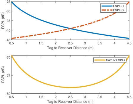
3.16 Calculation of the Free-Space Loss (FSPL), in the single carreir setup, for the forward link and the backscatter link. . . 39
3.17 Possible setup of a distributed backscatter system. Patch antennas are represented in the transmitters, and omnidirectional antennas are represented in the receiver and in the possible tag locations. . . 40
4.1 Example of a Simulink model capable of receiving samples from the Software Defined Radio (SDR) pen. . . 42
4.2 Implemented pipeline, for the transport of data between SDR pen, GNU Radio, First In First Out (FIFO) and Matlab. . . 44
4.3 Flowgraph of the GNU Radio’s processing blocks with their parameters exposed. . . 45
List of figures
4.5 Voltage signal applied to the transistor’s gate, with the backscatter tag programmed to switch between bit ’0’ and bit ’1’ , with 1 cycle of sleep time between commutations. . . 47 4.6 Voltage signal applied to the transistor’s gate, with the backscatter
tag programmed to switch between bit ’0’ and bit ’1’ , with 8 cycles of sleep time between commutations. . . 47 4.7 Complex numbers represented in Polar and in Cartesian form . . . . 48 4.8 Indoor single setup, with a distance of each system’s element of 0.5m
to the tag. . . 50 4.9 Received samples of a Binary Phase Shift Keying (BPSK)
transmission, represented in a complex plane, normalized. . . 51 4.10 Illustration of a BPSK transmission, without noise, with transmitter
and receivers out-of phase oscillators, throughout time. Said symbols, in a constellation plot, are not equidistant to the center . . . 51 4.11 Illustration of a decimation process applied to a signal. At the left is
represented the original signal with a sampling rate of Fs and at the
right the decimated signal with a new sampling rate of Fs/2. . . 53
4.12 Frequency response of the low pass filter, with a passing bandwidth of 4kHz. . . 53 4.13 Received signal’s spectrum (in baseband). . . 54 4.14 High Pass Filter (HPF) frequency response . . . 55 4.15 Example of a received signal with low noise. From top to bottom:
signal before HPF and signal after HPF. . . 56 4.16 Received signal with motion effects. . . 56 4.17 Received signal with motion effects, filtered with a HPF. . . 57 4.18 Reception of the payload "0,1,0,1,0,0". Top figure presents a signal
that was not filtered by HPFand bottom figure displays a signal that was filtered with the HPF . . . 58 4.19 Exemplification of the match’s filter application, where (a) represents
input signal, (b) is the rectangular’s pulse image, and (c) is the match’s filter output. Source: [91] . . . 59 4.20 Simulation of the Match Filter (MF)’s output of the signal obtained
by coupling every data combination with the preamble ’001111110’. For viewing purposes only 3 packets are displayed . . . 60 4.21 Response of the preamble’s MF, to a filtered received signal. . . 60 4.22 Plot of the receiver’s ability to reconstruct the transmitted binary signal 61
4.23 Plot of the received signal, the reconstruction performed by the receiver and the sampling instants obtained thought the MF preamble
reference. . . 62
4.24 Simulation of both MF’s response for a signal with two different preambles. . . 63
4.25 Spectrum of the three carriers. . . 64
4.26 Complete processing chain. . . 65
5.1 Indoor single carrier setup. . . 68
5.2 Indoor single carrier Bit Error Rate (BER) measurements for several transmitter’s output power. . . 69
5.3 Indoor single carrier Packet Error Rate (PER) measurements for several transmitter’s output power. . . 70
5.4 Indoor single carrier setup, translated 60cm. . . 70
5.5 Outdoor single carrier setup . . . 71
5.6 Bit Error Rate of the outdoor single carrier setup, in which the tag is positioned between the transmitter and the receiver. For each transmission output power, a sweep of the tag’s positioning was realized. 72 5.7 Packet Error Rate of the outdoor single carrier setup, in which the tag is positioned between the transmitter and the receiver. For each transmission output power, a sweep of the tag’s positioning was realized. 72 5.8 Calculated power at the receiver with the correspondent errors measured in Figure 5.6. . . 73
5.9 Setup for longer distances measurements. . . 73
5.10 Bit Error Rate of the outdoor single carrier setup, in which the tag is positioned between the transmitter and the receiver. The transmitted power is fixed at 10 dBm and the transmitter’s position is placed at 15 m, 20 m and 25 m from the receiver. . . 74
5.11 Packet Error Rate of the outdoor single carrier setup, in which the tag is positioned between the transmitter and the receiver. The transmitted power is fixed at 10 dBm and the transmitter’s position is placed at 15 m, 20 m and 25 m from the receiver. . . 75
5.12 Calculated power at receiver with the power level at which error starts to manifest. . . 75
5.13 Distributed Setup . . . 76
5.14 Distributed setup applied to the laboratory. . . 78 5.15 BER measurements of the distributed setup applied to the laboratory. 79 5.16 PER measurements of the distributed setup applied to the laboratory. 79
List of figures
A.1 Block diagram of a FIR filter . . . 86 A.2 Block diagram of a FIR filter. Source [95]. . . 87 B.1 Illustration of an Amplitude Shift Keying (ASK) modulated carrier.
Adapted from [96]. . . 89 B.2 Illustration of a ASK modulated signal spectrum . . . 90 B.3 Illustration of an Phase Shift Keying (PSK) modulated carrier.
List of tables
2.1 Power sensitivity of commercial passive tags for reading operation.
Source: [23–29]. . . 9
2.2 Specifications of diverse commercial Ultra High Frequency (UHF) readers [49–54]. . . 15
2.3 Comparison between Wideband Software Defined Radios available in the market. Source:[57–60]. Values . . . 16
5.1 Reception test for one carrier. . . 77
5.2 Reception test for two carriers. . . 77
List of abbreviations
µC MicroController
ADC Analog-to-Digital Converter
ANACOM Autoridade Nacional de Comunicações ASK Amplitude Shift Keying
BB Base Band
BER Bit Error Rate BPF Band Pass Filter
BPSK Binary Phase Shift Keying CCS Code Composer Studio CFO Carrier Frequency Offset CRC Cyclic Redundancy Check
CW Continuous Wave
DAC Digital-to-Analog Converter
DBV-T Digital Video Broadcasting - Terrestrial DC Direct Current
DETI Departamento de Eletrónica, Telecomuncações e Informática DSP Digital Signal Processor
EB Evaluation Board EH Energy Harvesting
EIRP Effective Isotropic Radiated Power EM Evaluation Module
ENOB Effective Number of Bits EPC Electronic Product Code ERP Effective Radiated Power
FCC Federal Communications Commission FDMA Frequency Division Multiple Access FHSS Frequency Hopping Spread Spectrum FIFO First In First Out
FIR Finite Impulse Response FM Frequency Modulation FSK Frequency-shift Keying FSPL Free-Space Loss
FSPL-BL Free-Space Loss Backscatter Link FSPL-FL Free-Space Loss Forward Link HEMT High Electron Mobility Transistor
HF High Frequency
HPF High Pass Filter
I2C Inter-Integrated Circuit IC Integrated Circuit
IDE Integrated Development Environment IF Intermediate Frequency
IFF Identification Friend or Foe IIR Infinite Impulse Response IoT Internet of Things
IQ In-Phase and Quadrature
ISO Internation Organization for Standardization IT Institute of Telecommunications
ITU International Telecommunication Union
LF Low Frequency
LNA Low Noise Amplifier LO Local Oscillator LPF Low Pass Filter
MF Match Filter
MOSFET Metal Oxide Semiconductor Field Effect Transistor MSc Master of Science
NDA Non Disclosure Agreement
OC Open Circuit
List of abbreviations
OOT Out of Tree
OS Operative System
OSI Open Systems Interconnection PCB Printed Circuit Board
PER Packet Error Rate PLL Phase-Locked Loop PPreamble Packet Preamble PSK Phase Shift Keying
QAM Quadrature Amplitude Modulation
RF Radio Frequency
RFID Radio Frequency Identification
SC Short Circuit
SDR Software Defined Radio SNR Signal to Noise Ratio
TDMA Time Division Multiple Access TI Texas Instruments
TxPreamble Transmission Preamble UHF Ultra High Frequency USA United States of America USB Universal Serial Bus
USRP Universal Software Radio Peripheral VCO Voltage Controlled Oscillator
VGA Variable Gain Amplifier WPT Wireless Power Transfer WSN Wireless Sensor Networks
Chapter 1
Introduction
In this chapter the driving force for the use of energy efficient communications systems in the paradigm of world sensorization will be presented, as well as the objectives proposed for this Master of Science (MSc) dissertation. Moreover a brief history section of the evolution of systems, that have as their cornerstone reflected radio waves, will be described and finally, the main contributions from this work will be detailed.
1.1 Background and Motivation
Technology has been responsible for changing the human everyday life and in the vast majority, the changes have been greatly positive. The constant evolution of technology has brought another concept at our doorstep: Internet of Things (IoT). One way to define IoT is as follows: "An open and comprehensive network of intelligent objects that have the capacity to auto-organize, share information, data and resources, reacting and acting in face of situations and changes in the environment" [1].
It aims for a global infrastructure that allows us to know the state of the world around us and the capability to actuate on it, having useful applications in a diverse spectrum of areas including: medical, manufacturing, industrial, transportation, education, etc. According to International Telecommunication Union (ITU) [2], the reference model of the IoT is comprised by several layers: Application layer, Service support and Application support layer, Network layer, and Device layer, which is similar to the Open Systems Interconnection (OSI) model in the area of networks. Focusing the Device layer, there is a need to implement sensors in a mass scale and a need to develop means to transport their information to the internet, via gateways. This units responsible for sensing the world around us, need power sources
in order to operate, which normally are batteries due to their reduced size and portability. However it is expected that the number of IoT connected devices, in the year 2025, achieve the mark of 75.44 billion devices worldwide [3]. In the event, that every device has a battery to supply energy, the upkeep of the global infrastructure will become unbearable, on the grounds that the batteries have not enough energy to supply the devices for long periods of time (some devices have a life expectancy of 3 to 5 years [4]). To tackle this problem the scientific community is focusing efforts in decreasing the amount of power that this devices use, which can be achieved, for example, by more energy efficient sensors, low power microcontrollers and backscatter modulation, being the latter the cornerstone of this dissertation. Backscatter modulation consists in the controlled reflection of a incident radio signal, in order to communicate. Another possible solution to overcome the energy limitations is the use of Wireless Power Transfer (WPT) as elucidated in [5] or Energy Harvesting (EH) such as [6] which are both concepts out of the scope of this work but are presented for informative purposes. Principally EH since it allows the functioning of battery-less devices, or it can be combined with batteries to extend the batteries’ lifetime.
Besides the low life expectancy, that is a direct consequence of the limited energy available to the devices, another characteristic that is constrained is the area coverage that Wireless Sensor Networks (WSN) can achieve.
1.2 The evolution of reflected radio signal based
systems
Before addressing the technical aspects presented in this MSc dissertation, and mostly explained in Chapter 2, it is important to know their origin.
The advance of any radio transmission stands in the shoulders of giants such as Michael Faraday, which proposed in 1846 that both light and radio waves are part of electromagnetic energy [7]. Moreover, James Clerk Maxwell concluded in 1864, that electric and magnetic energy travels in transverse waves at the speed of light [8]. Another example is Hertz, which was the first to transmit and receive radio waves [9]. The radar was invented approximately in 1935 and further developed by the military during World War 2, which consists in sending radio waves that collide with objects and are scattered. The reflected waves provide information such as the distance that the objects are from the radar and their velocity. One of the problems that occurred at the time was the inability to assert if the incoming airplane was an ally or a foe. To solve this problem, the Germans rolled their planes when
Chapter 1. Introduction
returning to the base. They discovered that if the pilots rolled their planes, it provoked a pattern in the reflected radio waves, providing with a mean to identify the planes’ affiliation [10]. The British introduced in 1939 the Identification Friend or Foe (IFF), which consisted in sending signals from the ground stations to the aircraft. The planes had a set of receivers that at detecting the ground station signals, replied by sending an encoded signal at the same frequency, successfully identifying the aircraft [11]. This mechanism is very similar to a Radio Frequency Identification (RFID) system, which is composed of two essential components: a reader which is responsible for sending radio signals to a tag and receives the tag’s response, and a tag that holds the desired information and relays it to the reader when requested[12].
1.3 Objectives
The focus of this dissertation relies on the development of a low power distributed backscatter system capable of sensing, data transfer through backscatter techniques, data demodulation in order to achieve the maximum coverage range while consuming low power. This work is a proof of concept to determine the feasibility of such a system. More specifically, the objectives of this work are as follows:
• Understand passive and semi-passive backscatter communications. • Study of backscatter modulation.
• Implement a backscatter system.
• Receive the backscattered radio signals via SDR pen.
• Process and demodulate the information relayed by the SDR pen.
• Implement a distributed backscatter system with the carriers in different frequencies.
• Test the limits of communication distance and successful transmission as a function of transmitted signals power.
1.4 Contributions
The work developed in this MSc dissertation achieved all the proposed objectives in the section 1.3, which resulted in the following contributions:
• A Matlab application that demodulates backscattered modulated signals was developed.
• A bistatic dislocated backscatter communication system for a Continuous Wave (CW) source was achieved.
• A distributed system that allows the extension of the area where the tag can be located by implementing multiple carrier sources multiplexed in frequency was implemented and tested.
• A contribution for the article entitled "Performance evaluation of backscatter modulation techniques by using one and two frequencies" was realized, for the 2019 IEEE International Conference on RFID Technology and Applications. • An article was submitted to the IEEE Access Journal, entitled "Distributed
Chapter 2
State of the Art
This chapter presents the state of the art of several areas/technologies such as RFID, backscatter, and SDR. Moreover, in each section, there will be an explanation of concepts to provide the background needed to analyse the work developed in this dissertation.
2.1 Radio Frequency Identification
RFID systems allow for the identification of objects in an automated and wireless manner. This is an incredible advantage and has impacted many sectors, being the more natural application tracking and identification in warehouses and big retailers [13]. However, the applications are limitless, and these systems can be used in railways where RFID is used to monitor rail cars in a large area of tracks [13] or in lumberjack companies where it improves the tracking of wood logs reducing the loss of the assets in 70 % [14]. RFID is even applied at hospitals, where it improves the allocation of beds through a patient tracking system, and consequentially increases the hospital revenue [15].
A RFID system is comprised of two parts, as depicted in Figure 2.1: a tag (also known as a transponder), which is associated with an object and a reader which interrogates the tag and receives its response using radio signals [16]. These tags can send information through backscatter modulation, which consists of reflecting or not the readers’ radio signals or through radio signals generated at the tag. Moreover, the types of tags that use backscatter modulation are exposed in Section 2.1.2, and the theory behind this type of modulation is presented in Subsection Section 2.4.
RFID systems can be classified depending on a multitude of parameters such as the frequency of the system, the tag’s power source, if the power source is the reader, how the reader provides power, the tags storage type, among others. Since
Figure 2.1: Typical RFID architecture. Source: [16]
this dissertation focuses on radio backscatter, systems like inductive and capacitive RFID are not going to be presented as they do not fall in the scope of the dissertation.
2.1.1 Standards - Frequency and power norms
Regarding the first classification there are several radio frequency bands for the RFID technology: the Low Frequency (LF) band which is comprised between 125 kHz and 134 kHz, the High Frequency (HF) band where systems operate at 13.56 MHz, the UHF that covers the frequencies between 860 - 960 MHz and finally the two microwave bands which are stipulated in the range of 2.4 - 2.5 GHz and 5.725 - 5.875 GHz [12, 13, 17]. Taking a closer look at the UHF band, two different standards regulate this band throughout Europe and the United States of America (USA), which are respectively the European Telecommunications Standards Institute (ETSI) and the Federal Communications Commission (FCC). The RFID readers usually operate without a license, but they do have to respect certain restrictions that include frequency, power radiated, channel bandwidth, and operation scheme.
The ETSI regulates that RFID systems can be operated in the frequency band of 865 - 868 MHz radiating 2 W Effective Radiated Power (ERP) and in the frequency band of 915 - 921 MHz with power levels of 4 W ERP [18]. On the other hand, the FCC stipulates that the frequency of operations must be located between 902 -928 MHz while the radiated power varies, with the method of signal transmission. The norm section 15.247 [19] published by FCC states different maximum power
Chapter 2. State of the Art
levels in reference to the transmission method: a transmission with Frequency Hopping Spread Spectrum (FHSS) has a maximum output power of 1 W, if the system uses more than 50 channels and 0.25 W if the system employs a number of channels comprised between 25 to 50. If the system uses digital modulation, the maximum output power is 1 W. The values of the FCC are limited to the use of antennas that do not exceed 6 dBi, which is equivalent to stating that the maximum output power, for a system employing 50 channels, is 4 W Effective Isotropic Radiated Power (EIRP). Although the two standards define power in different ways, it is crucial to understand the differences. EIRP, as previously stated, stands for Effective Isotropic Radiated Power, which is "the amount of power that would have been radiated by an isotropic antenna to produce the peak power density observed in the direction of maximum antenna gain" [20] and it is calculated as in Equation (2.1).
EIRP = Pt∗ G (2.1)
Another way to express radiated power is by using ERP, which is calculated in reference to a half-wavelength dipole instead of the EIRP isotropic antenna. The two terms are related by the gain of the half-wavelength dipole, which is 1.6 in linear scale or 2.15 dBi in the logarithmic scale.
ERP(dBW ) = EIRP (dBW ) − 2.15 dBi (2.2)
To analyse the different power metrics used by ETSI and FCC, the following equations are used:
ERPetsi = 2W = 10log10(2) dBW;
ERPetsi = 3 dBW = 33 dBm;
EIRPetsi = ERPetsi+ 2.15;
EIRPetsi = 33 + 2.15 = 35.15 dBm;
EIRPf cc = 4 W = 10log10(4) dBW;
EIRPf cc = 6 dBW = 36 dBm;
EIRPf cc− EIRPetsi= 0.85 dB;
(2.3)
Analysing Equation 2.3, it is clear that the power between the two standards varies in 0.85 dBi or in ≈ 1.22 times. It is important to state that although these
entities define the standards, it is up to each countries telecommunications regulator to decide if they follow these guidelines. In the case of Portugal, the entity that regulates the spectrum is Autoridade Nacional de Comunicações (ANACOM), and it follows ETSI norms, which as previously stated, is 2 W ERP in the band of 865 -868 MHz and 4 W ERP in the band of 915 - 921 MHz or respectively 35.15 dBm and 38.15 dBm EIRP.
2.1.2 Power source
In order to implement RFID identifying systems in large factories and big supply chains, an enormous amount of tags must be deployed, which elevates the cost of the operation. Naturally removing batteries or Radio Frequency (RF) components from a tag reduces its price, making more alluring the technology.
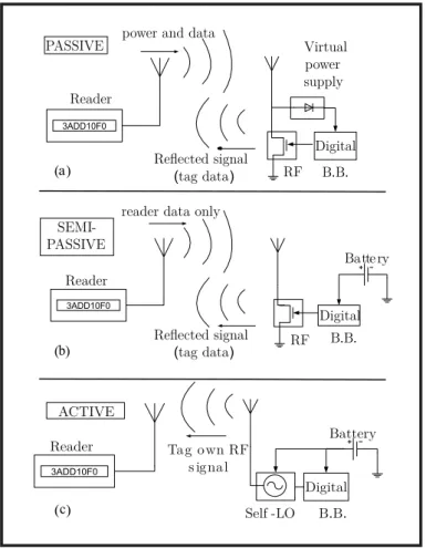
Figure 2.2: Tags classifications in function of the power supply method: a) Passive, b) Semi-passive, c) Active. Source: [21].
Having this said, it is possible to classify the tags depending on its components, or more precisely, on its power source. A typical tag is composed by an
Chapter 2. State of the Art
Integrated Circuit (IC) that controls the tag’s functionality and stores the desired information, an antenna that receives and transmit data, and a power source or/and a mechanism to harvest energy to operate the tag. Along with the explanation of the classifications, there are going to be presented some tags that fall in the respective category with an overview of their features.
Passive
As the name implies and as can be observed in Figure 2.2 a), passive tags have no battery. Despite the lack of power supplies inside the tag, they harvest energy from the reader’s radio signals when it interrogates the tag. This harvesting is realized by a RF-Direct Current (DC) converter to supply the circuitry with sufficient energy, allowing the logic unit of the tag to operate and consequently provide the reader with the desired information [22]. As the energy harvested is scarce due to FSPLs, mismatch losses, and RF-DC converters efficiency, backscatter modulation is implemented to reduce energy consumption.
Tag IC Power Sensitivity (dBm)
Impinj Monza 5 -17.8 Impinj Monza R6 -22.1 Impinj Monza X-8K Dura -19.1/-26.1 1 Alien Higgs 4 -18.5 Alien Higgs 9 -22.5 NXP UCODE DNA -19 NXP UCODE 8/8m -23
Table 2.1: Power sensitivity of commercial passive tags for reading operation. Source: [23–29].
In [30], a passive transponder is presented with a reading distance of 4.5 m with a 500 mW ERP base station transmit power, at the frequency of 868 MHz, in an anechoic chamber. The authors expect that if they follow the maximum power allowed in the USA, which as previously stated is 4 W EIRP, the RFID transponder could achieve 9.25 m. Passive tags are also able to identify moving objects as [31]’s tag can achieve 10 readings at 2 m/s, in a reading range of 0.5 m, with an antenna beam width of 80°. The reader used for [31] was a commercial one, yet it was not displayed any information on its specifications or brand. Nowadays, the great majority of commercial UHF RFID tags are passive, due to their low cost and
some of the IC of those tags can be found in Table 2.1 with their respective power sensitivity. The majority of passive tags available at the market, use one of the ICs(or a version of it) presented in this table. This means that their sensitivity does not deviate from the range of −17 to −23dBm.
Semi-passive
Similarly to passive tags, semi-passive tags also use backscatter modulation to reflect the reader signal to transmit information, a concept that is further explained and dissected in Section 2.4. They may or may not harvest energy, but they do have a battery to power the tag’s circuitry, as depicted in Figure 2.2b), being the semi-passive tags also known as battery-assisted tags [13, 32]. The presence of a battery implies that the lifetime of the tag is limited, principally if there is not an energy harvesting mechanism. In [33] a 2.4 GHz RFID IC tag was presented, that achieves a sensitivity of −19 dBm with a measured standby current of 700 nA at 1.5 V battery voltage. It is expected that the tags lifetime exceeds 10 years and achieves a range of 3.5 m. Another example of a semi-passive tag is presented in [34], where a tag was developed to operate at 10 GHz (X frequency band), which was powered by a battery of 3 V. The novelty of this tag, besides the frequency, was that the tag was designed on a flexible substrate. The distances between the tag to the transmitter and the tag to the receiver were the same: 0.5 m. A commercial semi-passive tag used for people tracking, is presented in [35] achieving a reading range of 5 m. It has a life expectancy of 2 years.
Active
Active tags are tags that use a battery to supply the radio module and the logic unit. These tags have local oscillators to create their carrier and can change channels to communicate while being near other tags, to guarantee non-collision [13]. The most significant advantage active tags have is the capability to achieve greater tag-reader distance as they do not have to backscatter the reader’s radio signals [36]. Backscatter communication implies that the reader’s radio signal needs to travel to the tag and back, while in an active tag, the radio signals only need to course through the tag-reader distance [17]. Having a communication module in a tag, which includes radio receiver and transmitter, allows the tag to implement more sophisticated modulations such as FSK, PSK, Quadrature Amplitude Modulation (QAM), modulation schemes that grant the system the capability to send information in higher data-rates while being more noise-resilient [13]. However there were not found active tags for the UHF band. Moreover, only
Chapter 2. State of the Art
in the 433 MHz and in the 2.45 GHz were found active tags. These tags have a reported maximum reading ranges, that vary between 40, 60, 80, 100 and 150m for the 433 MHz band [37] and 30, 80, 100 and 150m for the 2.45 GHz [38]. Their batteries life expectancies vary from 2 years up to 4 years.
There are also RFID tags that already are accompanied by a specific sensor, and it is the sensor information that is transmitted instead of a identification code. These tags can be passive,semi-passive or active tags, and are used to monitor temperature, humidity, motions and magnetic conditions. The sensor based RFID passive tags have a maximum reading range of 9m [39, 40].
High Order Modulation
Some works also tackle backscatter tags from a High order modulation perspective. These tags can backscatter data through QAM modulation, which increases the data rate of the sensors. The traditional approach, as already presented, is to use ASK, PSK or FSK, modulations that can transfer one bit per symbol period. With the novel approach of QAM backscatter tags, the data rate of low power consuming tags increases. In [41] a 4-QAM backscatter modulator was developed, that achieves a bit rate of 400 kbps at a static power of 115 nW. For greater data rates, [42] presented a backscatter tag that implements 16-QAM. This tag achieves 120 Mbps while spending 16.7 pJ/bit. Moreover an impedance modulator front-end was developed in [43], that is able to backscatter In-Phase and Quadrature (IQ). Due to its versatility, it was also used as a LoRa backscattering device, for the 2.45 GHz band. The device requires an SNR of −6.8 dB considering a BER of 10−3.
2.1.3 Communication Protocols
Protocols are needed to specify how the tag and reader communicate, which type of data encoding, the messages that are exchanged between the two counterparts, the code that identifies the tag (also known as serialization), among others. Some of the standards used in RFID are the EPCglobal, ISO, and ANSI [44]. Although the work developed in this dissertation did not implement any standard, it is required to understand their inner workings. The most used protocol in UHF frequencies, is the ISO1800-6C, used for passive tags. This specific standard is the result of the inclusion of the standard EPC Gen 2 Class 1, developed by EPCglobal, with the standard ISO1800-6, developed by Internation Organization for Standardization (ISO), allowing more unified guidelines for companies to develop RFID systems [45].
Figure 2.3: Electronic Product Code basic structure. Source:[46]
The standard defines an Electronic Product Code (EPC) for each tag that follows the structure represented in Figure 2.3, taking into account the class of the product associated with the tag, the company responsible for the definition of the object class and serial number, the version of the EPC, and the unique serial number, among others. It also specifies the exchange messages between the reader and tag and the timing of those messages, as can be perceived in Figure 2.4, where a single tag interrogation process is displayed.
Figure 2.4: EPCglobal Gen 2 Single tag message protocol, where RN16 is a random number of 16 bits, PC is a information for protocol control, EPC is an identification number (see Figure 2.3), XPC is an optional protocol control information and PacketCRC is a 16 bit CRC code. Source:[47].
2.2 Reader
RFID readers are radio transceivers that have their antennas configured in a monostatic configuration. This antenna arrangement means that the reader only has one antenna to transmit and receive signals. The vast majority of commercial readers are monostatic since the reduction of antennas lowers the complexity and cost of the reader. If the reader targets are semi-passive or passive tags, the interrogator needs to send a CW to energize the tags, while receiving the tags information.
Chapter 2. State of the Art
When a radio is simultaneously sending and receiving information, it is classified as a full-duplex radio. When only one of the operations can be realized at a specific time, the transceiver is labeled as a half-duplex radio [13]. One particularity of monostatic readers, is that part of the transmitted signal leaks into the reception, degrading the quality of the receiving tag information.
Receiver architecture
A radio receiver can have multiple architectures concerning frequency conversion. The transmitted baseband signals are mixed with a carrier of significantly higher frequency, and it is the receiver duty to convert the input signal to baseband again. For this purpose, there are direct conversion receivers and multiple conversion receivers, which are also known as, respectively, homodyne and heterodyne architectures.
Figure 2.5: Radio receiver architectures ((a) homodyne and (b) heterodyne) complemented with and Analog-to-Digital Converter and a Digital Signal Processor. Source:[46].
As depicted in Figure 2.5 (a), the homodyne receiver applies a Band Pass Filter (BPF) to eliminate noise and other unwanted signals, centered at the carriers frequency. A Low Noise Amplifier (LNA) amplifies the filtered signal reducing the noise introduced due to the amplification. Conventional amplifiers amplify the signal and the noise associated while introducing noise inherent to the amplifier. However
LNA are designed to minimize that inherent noise resulting in a better noise figure of the radio chain. Following the LNA, the mixer creates two spectral replicas of the input signal displaced in frequency by the Local Oscillator (LO) as Equation (2.4) shows:
RFin(t) ∗ LO(t)
= A(t)[cos(2πf1t) ∗ cos(2πf2t)]
= A(t)[cos(2π(f1 + f2)t) + cos(2π(f1− f2)t)]
(2.4)
If the LO has the same frequency as the carrier of the transmitted signal, the resulting replicas are A(t) + A(t)cos(2π(f1 + f2)t), that will be filtered by the Low
Pass Filter (LPF) and result in the baseband signal. This baseband signal will then be fed to an Analog-to-Digital Converter (ADC), which will output the digitalization of the analogue information. This digital sample can be further processed in the Digital Signal Processor (DSP). The heterodyne receiver diverges in relation to the
homodyne in the number of conversions. The heterodyne first converts the signal
to an Intermediate Frequency (IF) between RF and Base Band (BB), which allows the application of sharper cutoff filters. After this, the receiver converts the filtered signal to baseband. The conversion to an IF and the consequent possibility to use sharper filters improves the selectivity of the receiver and allows the application of another amplification stage. A RFID reader can also be classified in relation to its receiver function. These parameters are enumerated and described in the following list:
• Sensitivity - A receiver sensitivity is defined as the minimum input signal power with a defined Signal to Noise Ratio (SNR), to decode the signal successfully [48]. However, in the literature, sensitivity is also used to define the minimum power level needed at the receiver, for successful signal reception [49–54]. In this work, sensitivity is used as the second definition.
• Maximum reading rate - Corresponds to the maximum rate that a reader can communicate with a tag. The higher this rate, the greater is the number of tags that a reader can communicate in a second [55].
• Maximum reading distance - Defines the maximum distance a tag can be from the reader to successfully receive the tags information. This metric depends on the reader’s transmitted power, on the type of tag, antenna gain, reader’s sensitivity, among others [13]
Chapter 2. State of the Art
In Table 2.2 are displayed some commercial readers with their specifications and price points. From the table, it is observed that readers are costly machinery with a reading range comprised between 5 and 9 m. Table 2.2 was elaborated taking into account UHF readers that are oriented to passive tags.
Reader TX
(dBm)
Sensitivity (dBm)
Max Read Rate (tags/sec) Max Read Distance (m) Power Consumption (W) Price (€)2 Zebra FX7500 31.5 -82 - - - 1080 ThingMagic Sargas 30 - 750 9 15 840 Impinj Speedway Revolution R220 30 -84 200 - 50.4 1000 Nordic id SAMPO S1 30 - - 5 7 680 216032 27 - 100 5 12 -Intel RSP H1000 31.5 -93.6 600 - 16 910
Table 2.2: Specifications of diverse commercial UHF readers [49–54].
2.3 Software Defined Radio
SDR is a term used to characterize a radio system which is capable of controlling some or all the functions of its physical layer, through software. These parameters can be frequency range, modulation type, output power, among others [56]. This term can be applied to radio transmitters and radio receiver, however, the SDR receivers are drawing an increased amount of attention due to their low price, and their capability to receive virtually any IQ modulated signal. Most of these SDR receivers can output the digitalized signals through an Universal Serial Bus (USB) interface (thus called SDR pens), making any computer a possible radio receiver. These SDR pens implement several functions such as amplification, frequency conversion, analogue filtering, IQ demodulation, among others. These SDR pens are also classified depending on their tuning frequency, sampling rates, the resolution of their ADCs, among others. The Table 2.3 provides several SDR pens available in the market, with their specifications and their cost .
2.4 Backscatter
Backscatter modulation is one of the essential concepts in which this dissertation is based. This modulation consists of changing the antenna impedance so that it can reflect or absorb radio signals. Controlling this behaviour means that the
2 Prices observed in 11/2019
SDR Tune Low (MHz) Tune High (MHz) RX Bandwidth (MHz) ADC Resolution (Bits) Transmit? (Yes/No) Price ($USD3) RTL-SDR 24 1766 3.2/2.56(Stable) 8 No ∼20 BladeRF x40 300 3800 0.16-40 12 Yes 480 Airspy Mini 24 1700 3 12 No 99 RSP1A 0.01 2000 Up to 10 8/10/12/14 (depends on RX Bandwidth) No 109
HackRF One 1 6000 20 8 Yes
(half-duplex) 340
Table 2.3: Comparison between Wideband Software Defined Radios available in the market. Source:[57–60]. Values
antenna transmits information encoded in a On-Off Keying (OOK) scheme, where the absorbing state represents the bit ’0’, and the reflecting state represents the bit ’1’ [61].
Reflection coefficient
It is important to understand how changing the antenna impedance provokes and varies the reflection and for this reason, the reflection coefficient concept is going to be presented4 using the Figure 2.6.
Figure 2.6: Transmission in a lossless line, terminated in a load impedance ZL.
Source:[62]
If an incident wave is generated by a source at z<0, then the incident voltage represented by V+
o e
−jβZ, where β is the phase constant, will be travelling along the
transmission line of impedance Z0. As the transmission line is lossless, the incident
wave will not be attenuated when travelling the line, or in other words, the coefficient
Chapter 2. State of the Art
of attenuation α = 0. The situation changes when the line is terminated in a load different of the characteristic impedance of the line ZL 6= Z0, because the ratio
between voltage and current must be ZL, which means that a reflected wave must
exist with the appropriate voltage to satisfy the new condition. The total voltage at any given point of the transmission line can then be represented by the sum of the incident and the reflected waves:
V(z) = Vo+e−jβZ+ Vo−ejβZ. (2.5)
Moreover, changing the impedance of the load will change the reflected voltage wave V−
o ejβZ, which is exactly what is intended. To better see how different line
terminations provoke different reflections (more importantly the magnitude of the reflections) more analysis is going to be performed at the transmission line, or more precisely at the load (Z = L). If the total voltage is a sum of incident and reflected waves, then the total current is also a sum of waves:
I(z) = V + o Z0 e−jβZ − V − o Z0 ejβZ = (Vo+e−jβZ− Vo−ejβZ) 1 Z0 . (2.6)
When relating the Equations 2.5 and 2.6 by the load impedance, at Z = 0 the following equation is obtained:
ZL= V(0) I(0) = V+ o + V − o V+ o − Vo− Z0. (2.7)
Which solved in function of the reflected wave V−
o , results in:
Vo−= ZL− Z0 ZL+ Z0
Vo+. (2.8)
Observing Equation 2.8 and manipulating it in order to obtain the ratio between the reflected wave and the incident wave, the voltage reflection coefficient is obtained Γ: Γ = Vo− V+ o = ZL− Z0 ZL+ Z0 . (2.9)
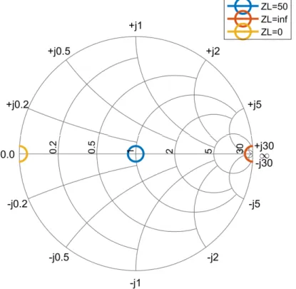
If the line is terminated in a Open Circuit (OC), which implies that ZL = ∞,
then the magnitude and the signal of the reflected voltage wave must be equal of the incident wave, so that the current is null. In this case the reflection coefficient Γ = 1. For a load impedance of ZL = 0, or in other words for a reflection coefficient Γ = −1,
the reflected voltage wave must be simetric to the incident voltage wave as to cancel both terms in the voltage equation, once that there is no load to produce a voltage potential. The other side of the coin is that the current is maximized as both terms
add in Equation (2.6). If the transmission line is adapted, then the load impedance
Figure 2.7: Different reflection coefficients for different load impedances, represented in a Smith Chart.
ZL is equal to the characteristic impedance of the transmission line Z0, and no
reflected wave is generated. This means that all the incident power is delivered to the load and nothing is reflected. The presented cases of loads impedance have their reflection coefficients depicted in Figure 2.7. As previously mentioned, the absorbing state refers to the bit ’0’, and the reflected state refers to the bit ’1’. The absorbing state naturally corresponds to ZL = 50Ω as the power that the antenna
receives is fully delivered to the load. The reflected state can be the result of the load impedance being any impedance different that of 50Ω.
Naturally, the greater the distance, in the Smith Chart, of the load, to the center, the greater the reflected power by the antenna. The ideal load would then be either Short Circuit (SC) or OC. This would implement an OOK/ASK modulation, as can be seen in Figure 2.8 a). Moreover, if the load impedance has an imaginary part, then the modulation implemented would be BPSK as the magnitude of the reflected power would be the same but the phase would be different (one example of BPSK is depicted in Figure 2.8).
Chapter 2. State of the Art
Figure 2.8: Constellation diagrams of: a) ASK and b) BPSK.
reflection coefficient for each state stands as [63]:
ΓA,B =
ZRF ICA,B − Z∗
ant
ZRF ICA,B + Zant
. (2.10)
and the amount of reflected power is proportional to a modulation factor, that takes into account the reflection coefficients of each state of the load:
M = 1
4|ΓA−ΓB|
2
. (2.11)
2.4.1 Backscatter Communication
There are several types of backscatter communication, which are classified depending on their antenna configurations or their carrier’s source. Ambient backscatter takes advantage of the already existing radio signals provided by Frequency Modulation (FM) Radios, Digital Television, and Wi-Fi, to perform backscatter.
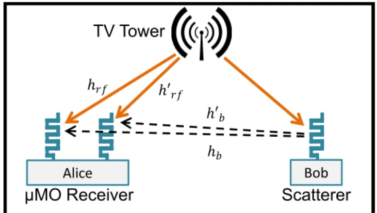
In [64] a ambient backscatter prototype was developed, that is able to cancel interferences using multiple antenna and to increase the communication range through the application of the µmo coding scheme, as exemplified in Figure 2.9. The TV signal, besides providing a radio signal to perform backscatter on, it also provides power for the receiver to operate. With a data rate of 1 MHz and a TV signal power of 0 dBm, a maximum distance of 18 m was achieved. Another example of ambient backscatter is presented in [65], where a 4-pulse amplitude modulation was used to backscatter information of a FM station. A power consumption of 20 µA was achieved, for a bit rate of 328 bps. The transmission was performed indoors,
Figure 2.9: A possible ambient backscatter architecture with two antennas for interference cancellation. Source [64].
with a transmission distance of 2 m, while the FM station was located 34 km away. However, if a carrier generator is used, there is more available power for the system to operate (since in ambient backscatters, the available power from existing radio signals is small). These systems are then classified, in relation to their antenna configurations, as monostatic and bistatic. RFID systems use monostatic configurations to decrease the price of the system (due to the reduction of the number of antennas), while academic works use bistatic configurations to increase the range of their systems5. Nonetheless, bistatic configurations are an approach used in
several works, such as [66], where a 246 m tag to reader distance was obtained, with a 13 dBm emitter transmission power. The carrier to tag distance was 3 m and the employed modulation scheme was FSK.
A OOK bistatic backscatter was analysed and implemented in [68]. They report a reading range of 60 m, when the backscatter tag is placed centimetres from the 30 dBm emitting carrier. Another example of bistatic backscatter is presented in [67] where a tag that employs FSK modulation is used (schematic presented in Figure 2.10). It achieves a communication distance of 3.4 km, with the tag placed at a distance of 1 m in relation to the 868 MHz carrier source. It also has a mode of operation, that allows the system to backscatter multiple Wi-Fi signals, where for each Wi-Fi radio a receiver is needed to process each frequency channel, located in the 2.4 GHz.
Only one work with a distributed approach was found, and is presented in [69]. They developed a system with multiple carriers, that sends CW’s , operating at 868 MHz, to several tags, and receives the backscatterd signal using a Universal Software
5Monostatic and bistatic configurations are presented in Figure 3.1 and explained in more detail
Chapter 2. State of the Art
Figure 2.10: Schematic of a FSK backscatter tag. Source: [67]
Radio Peripheral (USRP). All carriers are operating at the same frequency, and to avoid interference, the system implements Time Division Multiple Access (TDMA). Moreover the tags implemented employ a FSK scheme, where each tag has its own frequency associated, as exemplified at Figure 2.11. Although the receiver has to apply a correlation for each tag frequency (3 tags imply 12 filters), they are able to achieve a reading range of 150 m for BER of 5 %.
Figure 2.11: Spectrum of the FSK scheme employed in [69], where n corresponds to n tags.
Chapter 3
Backscatter Systems
In this chapter, different setups for backscatter transmission will be displayed, as well as the material used and their corresponding characterization. Power calculations were also realized to predict backscatter behaviours.
3.1 Backscatter setups
3.1.1 Single Carrier
As referred in Section 1.3, the core of this dissertation is to develop, in a first approach, a backscatter system capable of sending receiving information, very similar to a RFID system. There is a transmitter that sends a CW to a tag, and this tag performs backscatter modulation to send information to the receiver.
In Figure 3.1 are represented several configurations of antenna configurations. The monostatic link in Figure 3.1 a) is composed of two antennas, where one is connected to the RF tag and the other is connected to both transmitter and receiver. The bi-static link is a variation of the monostatic link, where the only difference lies in the separation of the transmitter and the receiver. In this way, an additional antenna is needed, as presented in Figure 3.1 b). As the transmitter and the receiver are placed side by side, this configuration is further classified as a Bistatic Collocated Link. Lastly, the Bistatic Dislocated Link is presented where the transmitter and receiver are positioned in end-points of the link, as observable in Figure 3.1 c) [70]. The work developed in this dissertation follows the bi-static dislocated link in order to avoid possible interference from the transmitter to the receiver. For this purpose, it was deemed appropriate to use antenna patches, for the receiver and transmitter, and one omnidirectional antenna for the tag. The omnidirectional antenna is the best choice for the backscatter tag because it is located between the transmitter
Figure 3.1: Three configurations of antenna in a backscatter link. Source [70]
and the receiver, and it needs to receive and reflect radio waves from both sides. At the opposite, the transmitter and receiver only need to send/receive electromagnetic waves in front of them, so their antennas can have a radiation pattern more focused, resulting in higher directivity and consequently, in higher gain in that direction [71]. The tag can be located anywhere between the transmitter and the receiver, as long as it is positioned inside the antennas area of coverage.
3.1.2 Distributed Carrier
If one transmitter and one receiver allows a tag to freely be positioned between them, then the implementation of various transmitters would allow a larger area where the tag could be positioned. This could be achieved if the receiver’s antennas were changed from a patch antenna to an omnidirectional one. Although this may be true, several barriers need to be addressed to successfully implement this architecture, such as the increased receiver complexity to accommodate information resulting from the backscattering of several carriers. Moreover, the interferences of multiple CW transmitters would create points in space where the signals would be cancelled. These problems are exposed and tackled in Section 3.4.
A possible setup of this distributed architecture would be composed by three carriers, one backscatter tag and one receiver, as illustrated in Figure 3.17.
3.2 Material
For the realization of this work three essential components were used: the transmitter, the receiver and the backscatter tag. Each and every one of this functional block has an antenna to allow the radiation of the signals. In this section the antennas are addressed first. Then the backscatter tag is presented, followed by the transmitter. The last component to be discussed is the receiver.
Chapter 3. Backscatter Systems
3.2.1 Antennas
In this work, no antennas were designed because there were already developed antennas in the Institute of Telecommunications (IT)’s possession that could be used in this dissertation, allowing time and resources to be focused in other areas. For the single carrier setup, it is needed two patch antennas and one omnidirectional. For the distributed setup, three patch antennas are required, as well as two omnidirectional antennas. As the patch antennas can be utilized in both setups, the total number of antennas amounts to three patch antennas and two omnidirectional antennas. The used antennas are shown in Figure 3.2 with their bandwidth exposed in the Figure 3.3.
Figure 3.2: One of the rectangular patch antennas and both omnidirectional antennas used in the system. From right to left: dipole antenna A, omnidirectional antenna B and omnidirectional antenna A.
Although in Figure 3.2 is only depicted one patch antenna, the remaining two are very similar, and for this reason only one patch antenna is showed in a representative way. Bandwidth can be defined in several ways and in this dissertation, [71]’s definition is adopted, which specifies that bandwidth is defined by a section of frequencies where the antenna has a reflection coefficient, S11 of less than −10 dB. In other words, it means that if a signal is injected into an antenna, only 10 %
or less of the signal, is reflected back. In the case of this antennas they all have similar bandwidths, making it possible to define a set of frequencies where all the antennas are adapted. This overlapping bandwidth is comprised between 864 and 865 MHz. To implement the system, the selected bands were 864 and 865 MHz which
Figure 3.3: S11 measurements of antennas used during this dissertation.
deviates from the frequencies allowed by ETSI and consequentially from ANACOM. However as this work is a proof of concept, the deviation of frequencies from the 864 and 865MHz band is not considered an infringement of regulations. These antennas were designed with a simulated gain of 6 dBi. To evaluate their practical gain of the patch antennas, measurements are needed to be performed in an anechoic chamber, using the reference antenna gain as basis. Moreover the available wideband antenna has an bandwidth of 0.7 and 18 GHz, which means that it is possible to measure the antenna gain. However analysing the antenna’s datasheet, the resolution of the gain chart, at the desired frequencies, is very low. To introduce the gain of the antenna for frequencies similar to 864 MHz, the gain is easily mistaken between 2.5 and 7.5 dBi [72], which brings great uncertainty to the measurements. For this reason the gain of the antennas was not measured and for all calculations that require the patch antenna’s gain, the simulated gain is used, which is 6 dBi. For the omnidirectional antenna A, as there is no model description or datasheet associated, the common value for dipole antennas, which is 2.1 dBi, is used [71]. For the dipole B the antenna gain is 4.5 dBi [73].
Chapter 3. Backscatter Systems
3.2.2 Backscatter tag
The semi-passive backscatter tag that is displayed in Figure 3.4, was developed by a colleague of the IT, and is composed of the following elements:
• Voltage regulator - an ultra low quiescent current1 voltage regulator
(NCP583) [75]. It ensures that whatever the way that the tag is supplied (battery, power supply, programming tool) the microcontroller receives a voltage inside the desired electric specifications. In this case the voltage required was 1.8 V.
• Ultra-low-power MicroController (µC) (MSP430F2132) which has a standby current consumption of 0.1 µA and a active mode consumption of 0.25 mA (at 1 MHz, 2.2 V [76]). It has in memory the packets needed to send and defines the data transmission rate. The µC feeds the DAC that will commute the transistor.
• 12 bit DAC (MAX555) which has an error of 1 % of full scale. It is used to control the voltage at the gate of the switching transistor [77].
• Crystal oscillator of 32.768KHz ±20E−6Hz(FC-135) [78]. It ensures that the
operating frequency of the microcontroller (which by consequence imposes the operating frequency of the tag) is lower than it would be, if the reference clock was the internal oscillator. This allows to reduce the energy consumption of the backscatter tag.
• Low noise HEMT (ATF-541433) [79]. It is a field-effect transistor that is designed to have better performance in higher frequencies than regular Metal Oxide Semiconductor Field Effect Transistor (MOSFET). It is used to change the impedance connected to an Antenna, or in other words, to perform backscatter modulation.
The µC is programmed using Code Composer Studio (CCS), through the MSP-FET430UIF. The CCS is an Integrated Development Environment (IDE) where it is possible to develop and debug embedded applications for Texas Instruments µC. The MSP-FET430UIF is a flash emulation tool that allows the CCS to flash the developed program into µCs and to implement debugging through the computer’s USB interface debugging. Figure 3.5 presents the chain of components used to toggle the impedance of the tag. The code developed in CCS outputs a digital
1Quiescent current is the current that a device uses when is in idle mode, i.e. when the circuit
Figure 3.4: Semi-passive Backscatter tag
Figure 3.5: Identification of various components pins. From left to right is indicated the digital pin 3, the DAC’s input pin, the DAC’s output pin, the copper connection under the PCB and the HEMT Gate pin.
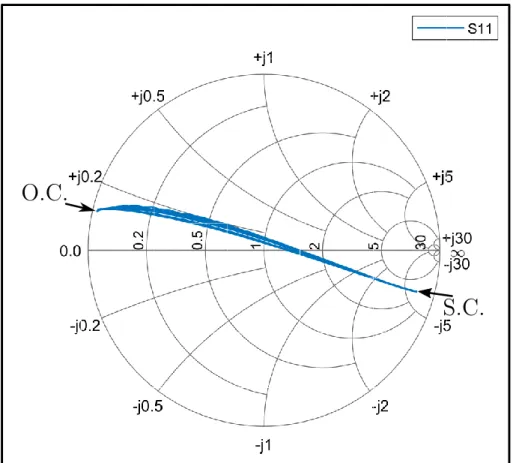
’1’ or ’0’ to the DAC which in turn changes the impedance at the tag’s output. When the µCs digital pin 3 outputs a bit ’1’ or a bit ’0’, it sets correspondingly, the DAC’s output to 0.6 V and 0 V, changing the state of the HEMT. The impedance change due to the transistor commutation is depicted in Figure 3.6, where is possible to observe that the S11 of the tag commutes between two regions of impedance. In addition, after the µC change the input of the DAC, it enters in a sleep state in order to decrease its power consumption, only waking when another change needs to be implemented.
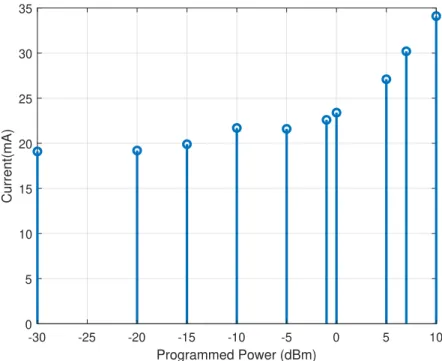
Important to note that, as the backscatter tag is driven by a 32 kHz clock, the maximum allowed data rate is bellow this value, as time is spent executing the µCs flashed code. The tag has a reported power consumption comprised between 39 and
Chapter 3. Backscatter Systems
Figure 3.6: Smith Chart of tag’s S11 parameters, in a frequency sweep comprised between 864 and 865MHz. O.C. stands for Open Circuit and S.C. stands for Short Circuit. Both states are relative to the transistor.
138 µA [80], for various bit and sleep periods.
3.2.3 Transmitter
For the transmitter it was needed a device that would be able to send a CW, coupled with the ability to control its frequency. It was initially predicted that the control of the frequency carriers, with a span of 1 MHz would be sufficient. In order to fulfil this specifications, a VCO was regarded as a possible solution. As the name implies, the frequency of oscillation is controlled by a voltage applied to the device. For this purpose a VCO was acquired with its corresponding Evaluation Board, which is displayed in Figure 3.7. The said oscillator is the CRYSTEK CVCO55CL-0800-0980, which has a frequency span of 180 MHz, comprised between 800 and 980 MHz. The oscillator requires a supply voltage of (5.00 ± 0.25) V and the frequency is controlled by varying the tuning voltage between 0.5 V and 4.5V. Moreover, one of the electric specifications of VCOs is the tuning sensitivity, which

![Figure 2.11: Spectrum of the FSK scheme employed in [69], where n corresponds to n tags.](https://thumb-eu.123doks.com/thumbv2/123dok_br/15849170.1085354/47.892.195.702.687.1010/figure-spectrum-fsk-scheme-employed-n-corresponds-tags.webp)