HOLOS, Ano 36, v.1, e8378, 2020 1
Novel Quantum Structure of an
III-V Tunneling Field-Effect
Transistor with Source and Channel Heterojunction
M. SABAGHIPhotonics and Quantum Technologies Research School, Nuclear Science and Technology Research Institute [email protected]
Received 08/03/2019 – Acepted 17/02/2020 DOI: 10.15628/holos.2020.8378
ABSTRACT
In this work, an III-V tunneling field-effect transistor (TFET) with source and channel heterojunctions is proposed and introduced. Proposed structure combine the high tunneling efficiency induced by heterojunction material and the high mobility of III-V material. The III-V TFETs based on either source heterojunction and channel heterojunctions have been intensively researched due to their excellent subthreshold-swing characteristics. However, compared with conventional V TFETs, the
III-V TFETs with source and channel heterojunctions have both shorter tunneling distance and two transmission resonances that significantly improve the on-current. The transfer characteristics affected by gate length were also evaluated. The results show that on-current, off-current, and on-current/off-current ratio and subthreshold-swing of III-V TFETs with source and channel heterojunctions are about 10-3 A/µm, 10-13 A/µm, 10-10 and 30
mV/decade, respectively.
KEYWORDS: III-V material, source heterojunction, channel heterojunction, Tunneling field-effect transistor (TFET).
Nova estrutura quântica de um transistor de efeito de campo de tunelamento
III-V com fonte e canal Heterojunction
RESUMO
Neste trabalho, um transistor de efeito de campo de tunelamento III-V (TFET) com heterojunções de fonte e canal é proposto e introduzido. A estrutura proposta combina a alta eficiência de tunelamento induzida pelo material de heterojunção e a alta mobilidade do material III-V. Os TFETs III-V, baseados em heterojunções de fontes e em heterojunções de canais, têm sido intensamente pesquisados devido às suas excelentes características sub-threshold-swing. No entanto, em comparação com TFETs III-V convencionais, os TFETs III-V com
heterojunções de fonte e de canal têm uma distância de túnel mais curta e duas ressonâncias de transmissão que melhoram significativamente a corrente em andamento. As características de transferência afetadas pelo comprimento da comporta também foram avaliadas. Os resultados mostram que a relação entre corrente, corrente fora de serviço e corrente/corrente fora de limite e TFETs de III-V com heterojunção de fonte e canal são de cerca de 10-3 A/µm, 10-13 A/µm , 10-10 e 30
mV/década, respectivamente.
Palavras-Chave: Material III-V, heterojunção de origem, heterojunção de canal, transístor de efeito de campo de tunelização (TFET).
HOLOS, Ano 36, v.1, e8378, 2020 2
1.
INTRODUCTION
Recently, tunneling field-effect transistors (TFETs) are emerged as the most attractive transistor due to their subthreshold-swing, leakage current and transconductance characteristics (Vallett, et al., 2010; Ionescu and Riel, 2011; Marjani, et al., 2016(a); Ameen, et al., 2019; Woo and Kim, 2019). Basically, the TFET is defined as a reverse biased gated p-i-n device, in which the gate controls the band-to-band tunnelling between the source and the drain through modulation of the position of energy bands. In order to occur band-to-band tunnelling in TFETs, several conditions need to be fulfilled (Ameen, et al., 2019; Marjani and Hosseini, 2015(b); Marjani, et al., 2017; Dorostkar and Marjani, 2018). At first, band alignment of source-channel interface and electron and hole layers of channel are formed properly. Second, the electric field is available at source-channel interface to reduce the tunnel barrier height and tunnel distance. Third, the electron and hole wave functions have significant overlap. Forasmuch as the valence band of source is lower than the conduction band of channel in off-state, very little current flows arising from the large tunneling barrier and distance between the source and channel. With applying the gate voltage in on-state, the energy bands of channel come down so that the conduction band of channel is located lower than valence band of source. In this way, the tunneling barrier has been eliminated and the tunneling distance has been shortened. These conditions cause the high electric field at the source-channel interface that forces the electrons to tunnel from the valence band of source to the conduction band of channel through the tunneling window between the source and the channel (Marjani and Hosseini, 2014(a); Marjani and Hosseini, 2014(b); Marjani, et al., 2017; Dorostkar and Marjani, 2018; Horst, et al., 2019).
On the one hand, the silicon-based TFETs have low on-current about 3 decades lower than metal-oxide-semiconductor field-effect transistor (MOSFET) that causes their less competitive in high-performance applications (Sabaghi et al., 2016(a); Sabaghi et al., 2016(b); Dashtbayazi et al., 2015; Das, et al., 2018; Ashita, et al., 2019; Marjani, et al., 2016(b); Marjani, et al., 2016(c)). A number of designs have been proposed to further improve the on-current of the silicon-based TFETs including band-gap engineering (Luisier and Klimeck, 2010; Das, et al., 2015), low band-gap materials (Ganapathi, et al., 2010), high-k dielectric materials (Marjani and Hosseini, 2014(a); Jain et al., 2015; Noor, et al., 2017), source–pocket doping (Chang, et al., 2013; Marjani and Hosseini, 2015(a); Marjani, et al., 2016(b); Marjani, et al., 2017), vertical direction tunneling (Alper, et al., 2018), and extended source (Marjani and Hosseini, 2014(a); Marjani and Hosseini, 2014(b); Marjani, et al., 2017). Another way to overcome this weakness and improve the on-current is replacng silicon with high mobility of III-V material (Marjani, et al., 2016(b); Dorostkar and Marjani, 2018). On the other hand, device geometries have been considered to boosting tunneling probability by employing heterojunction for the tunnel junction to reduce the tunnel barrier height and tunnel distance (Marjani and Hosseini, 2015(a); Marjani and Hosseini, 2015(b); Marjani, et al., 2016(b); Dorostkar and Marjani, 2018).
In this study, an III-V tunneling field-effect transistor with source and channel heterojunctions is proposed and introduced that combine the heterojunction and III-V materials. The simulations of proposed structure were performed by 2D device simulation to meet the
high-HOLOS, Ano 36, v.1, e8378, 2020 3
performance requirements predicted by the most recent technology roadmap. The model are given in section 2 and the proposed structures are reported in section 3. The results are discussed in section 4 and final conclusion in section 5.
2. MODEL
The carrier continuity equations for electron and hole are defined by (Atlas – Device Simulation Framework., 2018): 1 . n n n n G R J t q 1 1 . p p p p G R J t q 2
where n, p, Jn, Jp, Gn, Gp Rn, Rp and q are the electron concentration, hole concentration, electron
current density, hole current density, electrons generation rate, holes generation rate, electrons recombination rate, holes recombination rate and magnitude of the charge on the electron, respectively.
When a high electric field is available at source-channel interface, the carriers tunnel from from the valence band of source into the conduction band of channel. In the other words, an additional carrier is therefore generated in the conduction band that this generation is performed into the right-hand side of the above continuity equations. The nonlocal band-to-band tunneling model calculate a generation rate at each point based solely on the field value nonlocal to that point. Therfore, it need to take into account the spatial variation of the energy bands in order to model the tunneling process more accurately. The net current per unit area is (Atlas – Device Simulation Framework., 2018):
T T
T T(E) (E) (E E ) (E E )
(E ) dEdE
q
l r J T f f 3
where T(E) is the electron tunneling probability, E is longitudinal energy, ET is the transverse energy
and ρ(ET) is the 2D density of states. fl and fr is the Fermi-Dirac function using the quasi Fermi-level
on the left and right hand side of the junction, respectively. The equations of the quasi-Fermi level on the left hand side of the junction, the quasi-Fermi level on the right hand side of the junction, 2D density of states and the electron tunneling probability can be defined , respectively, by (Atlas – Device Simulation Framework., 2018):
HOLOS, Ano 36, v.1, e8378, 2020 4 1 1 exp T Fl l E E E f KT 4 1 1 exp T Fr r E E E f KT 5 T 2 (E ) 2 m me h 6 (E)exp2 ( )
end start x x T k x dx 7Where k is Boltzmann’s constant, T is temperature. me is the transverse electron effective mass,
mh is the transverse hole effective mass and h is Planck’s constant xstart is the start point of the
tunneling paths and xend is start and end points of the tunneling paths. k(x) is evanescent
wavevector at points and can be calculated as (Atlas – Device Simulation Framework., 2018):
2 2 ( ) e h e h k k k x k k 8
where Ke and Kh can be written as (Atlas – Device Simulation Framework., 2018):
0 1 ( ) 2 ( )( ( )) e e c k x m m x E E x i 9 0 1 ( ) 2 ( )( ( ) ) h e v k x m m x E x E i 10
where m0 is the rest mass of an electron.
In order to calibrate the nonlocal band-to-band tunneling model in the device simulation, should be specified the its values including the rest mass of an electron, electron effective mass and hole effective mass (Atlas – Device Simulation Framework., 2018). These values are 0.32, 0.55 and 0.25 for the electron effective mass, hole effective mass and rest mass of an electron to fit with the experimental data (Marjani and Hosseini, 2014(a); Marjani and Hosseini, 2014(b)). On the other hand, multiple models were included for higher reliability of device simulation results including the Auger recombination, band–gap narrowing, Hurkx and Shockley–Read–Hall (SRH) recombination, the concentration and field dependent mobility and trap–assisted–tunneling.
3. PROPOSED STRUCTURE
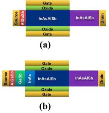
Figure. 1 illustrates a schematic view of the conventional III-V TFET and III-V TFET structure with source and channel heterojunctions, respectively. The body thickness and channel width are
HOLOS, Ano 36, v.1, e8378, 2020 5
both 10 nm. The channel length is 30 nm.Aluminum is used to form the gate electrode with work function of 4.2 eV and ZrO2 is applied to the gate insulator with permittivity of 29ε0. The gate oxide
is 2 nm. In III-V TFET structure with source and channel heterojunctions, the channel is made from a 3 nm InAs layer and a 12 nm InAsAlSb layer with doping density of 1×1016 cm−3. In addition, the
source are made from a 1.2 nm AlGaSb layer and a 3.3 nm GaSb layer with doping density of 5×10¹⁹
cm−3. The drain are made from 10 nm InAsAlSb layer with doping density of 2×1019 cm−3. On the
other hand, the added heterojunctions in the channel and source are InAs/InAsAlSb and AlGaSb/GaSb layers, respectively.
4. RESULTS AND DISCUSSION
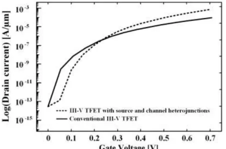
Figure. 2 shows gate voltage dependence of logarithm scaled drain current for the conventional III-V TFET and III-V TFET structure with source and channel heterojunctions with gate length of 30 nm biased at drain voltage of 1 V. It can be seen that by introducing with source and channel heterojunctions, III-V TFET structure with source and channel heterojunctions has a higher on–state current around 1 decade about 10-3 while maintaining off–state current of 10-13, resulting
in higher on-current/off-current ratio of 1010 as compared to conventional III-V TFET.Because of
Figure 1: Schematic view of (a) the conventional III-V TFET and (b) III-V TFET structure with source and channel heterojunctions.
HOLOS, Ano 36, v.1, e8378, 2020 6
Figure 2: The gate voltage dependence of logarithm scaled drain current for the conventional III-V TFET and III-V TFET structure with source and channel heterojunctions.
two additional heterojunctions (one in the source and the other in the channel), the tunnel barrier height and tunnel distance significantly reduced. On the other hand, the low mass of an electron and bandgap in material of source and channel heterojunctions, the tunneling probability is increased. Therefore, the III-V TFET structure with source and channel heterojunctions has a higher drain current due to the increased tunneling probability.In addition, increased tunneling
Figure 3: The gate voltage dependence of transconductances for the conventional III-V TFET and III-V TFET structure with source and channel heterojunctions.
probability induced by source and channel heterojunctions, causes smaller subthreshold-swing of 30 mV/decade can be achieved in the III-V TFET structure with source and channel heterojunctions in comparison with that of conventional III-V TFET.
HOLOS, Ano 36, v.1, e8378, 2020 7
Figure. 3 shows the comparison between the transconductances of the conventional III-V TFET and III-V TFET structure with source and channel heterojunctions with gate length of 30 nm biased at drain voltage of 1 V as a function of the gate voltage. As seen, the conductance of III-V TFET structure with source and channel heterojunctions increased by 450% at high gate voltage compared to that of the conventional III-V TFET because of the higher on-current.
In order to much better analysis of the performance parameters, the subthreshold slope was defined as the average slope between the off–state current and threshold current as below (Marjani, et al., 2016(b)): log th off th off V V SS I I 11
where Vth is the threshold voltage and defined here by the constant current method at the point
of 3×10⁻⁷ A/µm, I
off is defined to be the drain current at onset gate voltage, while on-currentis
defined at gate voltage of 0.7 V. These definitions are used in the rest of this paper.
In order to investigate whether the source and channel heterojunctions effects were present when the feature size of the devices decreased, the performances of the III-V TFET structure with source and channel heterojunctions with different gate lengths were also examined. Except gate length, all factors are kept as similar in these simulations. Figure. 4 shows the performance comparison of the logarithm scaled on–current as a function of gate length for III-V TFET structure with source and channel heterojunctions at drain voltage of 1 V. It is evident that the on-current (tunneling from source to drain regions) increases as the gate length decreases from 90 to 15 nm.
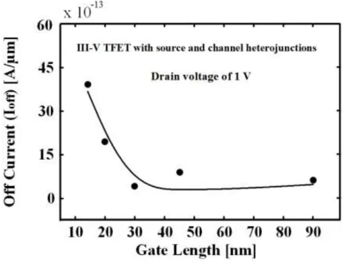
Figure. 5 shows the comparison of the off–current as a function of gate length for III-V TFET with source and channel heterojunctions at drain voltage of 1 V. As can be seen, variation in off-current is the dominant as compared with on-off-current. It should be mainly because of short-channel effects such as DIBL and charge sharing induced by down scaling of gate length.
HOLOS, Ano 36, v.1, e8378, 2020 8
Figure 4: The gate length dependence of logarithm scaled drain current for the III-V TFET structure with source and channel heterojunctions.
Figure 5: The gate length dependence of off-current for the III-V TFET structure with source and channel heterojunctions.
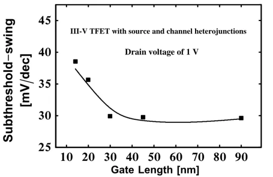
Figures. 6 and 7 show the plots for subthreshold-swing and on-current/off-current ratio as a function of different gate length for the III-V TFET structure with source and channel heterojunctions at drain voltage of 1 V, respectively. As can be seen, on-current/off-current ratio decreases and subthreshold-swing degrades with scaling down of gate length because of increasing off-current, as observed in Figure. 5.
HOLOS, Ano 36, v.1, e8378, 2020 9
25
30
35
40
45
10 20 30 40 50 60 70 80 90
Gate Length [nm]
Su
bt
hr
es
ho
ld
-s
wi
ng
[m
V/
de
c]
III-V TFET with source and channel heterojunctions Drain voltage of 1 V
Figure 6: The gate length dependence of subthreshold-swing for the III-V TFET structure with source and channel heterojunctions.
x 10
1010 20 30 40 50 60 70 80 90
Gate Length [nm]
O
n
-c
u
rr
en
t/
O
ff
-c
u
rr
en
t
R
a
ti
o
-0.3
0.0
0.3
0.6
0.9
III-V TFET with source and channel heterojunctions
Drain voltage of 1 V
Figure 7: The gate length dependence of on-current/off-current ratio for the III-V TFET structure with source and channel heterojunctions.
5. CONCLUSION
In this work, a detailed study of the III-V tunneling field-effect transistor (TFET) with source and channel heterojunctions is reported and introduced. The proposed structure is combination
HOLOS, Ano 36, v.1, e8378, 2020 10 of the high tunneling efficiency induced by heterojunction material and the high mobility of III-V material. The III-V TFETs with source and channel heterojunctions have both shorter tunneling distance and two transmission resonances as compared to conventional III-V TFETs, that significantly improve the on-current. Furthermore, the transfer characteristics affected by gate length were evaluated. The results show that on-current, off-current, and on-current/off-current ratio and subthreshold-swing of III-V TFETs structure with source and channel heterojunctions are about 10-3 A/µm, 10-13 A/µm, 10-10 and 30 mV/decade, respectively.
6.
REFERENCES
Alper, C., Padilla, J. L., Palestri, P., & Ionescu, A. M. (2018). A Novel Reconfigurable Sub-0.25-V Digital Logic Family Using the Electron-Hole Bilayer TFET. IEEE Journal of the Electron Devices
Society, 6, 2-7.
Ameen, T. A., Ilatikhameneh, H., Fay, P., Seabaugh, A., Rahman, R., & Klimeck, G. (2019). Alloy Engineered Nitride Tunneling Field-Effect Transistor: A Solution for the Challenge of Heterojunction TFETs. IEEE Transactions on Electron Devices, 66(1), 736-742.
Ashita, Loan, S. A., & Rafat, M. (2019). Insights Into the Impact of Pocket and Source Elevation in Vertical Gate Elevated Source Tunnel FET Structures. IEEE Transactions on Electron
Devices, 66(1), 752-758.
Atlas - Device Simulation Framework. (2018).
http://www.silvaco.com/products/device_simulation/atlas.html
Chang, H., Adams, B., Chien, P., Li, J., & Woo, J. C. (2013). Improved Subthreshold and Output Characteristics of Source-Pocket Si Tunnel FET by the Application of Laser Annealing. IEEE
Transactions on Electron Devices, 60(1), 92-96.
Das, G. D., Mishra, G. P., & Dash, S. (2018). Impact of source-pocket engineering on device performance of dielectric modulated tunnel FET. Superlattices and Microstructures, 124, 131-138.
Das, T., Jang, H., Bok Lee, J., Chu, H., Dae Kim, S., & Ahn, J. (2015). Vertical field effect tunneling transistor based on graphene-ultrathin Si nanomembrane heterostructures. 2D
Materials, 2(4), 044006.
Dashtbayazi, M., Sabaghi, M., & Marjani, S. (2015). Dynamic comparator with using negative resistance and CMOS input pair strategies in FS =4MHz-10GHz. Journal of Electrical and
Electronic Engineering, 3(4), 93–96.
Dorostkar, B., & Marjani, S. (2018). DC ANALYSIS OF p-n-p-n TUNNELING FIELD-EFFECT TRANSISTOR BASED ON In0.35Ga0.65As. HOLOS, 1, 288-296.
Ganapathi, K., Yoon, Y., & Salahuddin, S. (2010). Analysis of InAs vertical and lateral band-to-band tunneling transistors: Leveraging vertical tunneling for improved performance. Applied
HOLOS, Ano 36, v.1, e8378, 2020 11 Horst, F., Farokhnejad, A., Zhao, Q., Iniguez, B., & Kloes, A. (2019). 2-D Physics-Based Compact DC
Modeling of Double-Gate Tunnel-FETs. IEEE Transactions on Electron Devices, 66(1), 132-138.
Ionescu, A. M., & Riel, H. (2011). Tunnel field-effect transistors as energy-efficient electronic switches. Nature, 479(7373), 329-337.
Jain, P., Prabhat, V., & Ghosh, B. (2015). Dual metal-double gate tunnel field effect transistor with mono/hetero dielectric gate material. Journal of Computational Electronics, 14(2), 537-542. Luisier, M., & Klimeck, G. (2010). Simulation of nanowire tunneling transistors: From the
Wentzel–Kramers–Brillouin approximation to full-band phonon-assisted tunneling. Journal
of Applied Physics, 107(8), 084507.
Marjani, S., & Hosseini, S. E. (2014). Radio-frequency modeling of square-shaped extended source tunneling field-effect transistors. Superlattices and Microstructures, 76, 297-314. Marjani, S., & Hosseini, S. E. (2014). A novel double gate tunnel field effect transistor with 9
mV/dec average subthreshold slope. 2014 22nd Iranian Conference on Electrical Engineering
(ICEE).
Marjani, S., & Hosseini, S. E. (2015). Radio-frequency small-signal model of hetero-gate-dielectric p-n-p-n tunneling field-effect transistor including charge conservation capacitance and substrate parameters. Journal of Applied Physics, 118(9), 095708.
Marjani, S., & Hosseini, S. E. (2015). Analysis of radio frequency and stability performance on double-gate extended source tunneling field-effect transistors. 2015 23rd Iranian Conference
on Electrical Engineering.
Marjani, S., Hosseini, S. E., & Faez, R. (2016). A 3D analytical modeling of tri-gate tunneling field-effect transistors. Journal of Computational Electronics, 15(3), 820-830.
Marjani, S., Hosseini, S. E., & Faez, R. (2016). A silicon doped hafnium oxide ferroelectric p–n–p– n SOI tunneling field–effect transistor with steep subthreshold slope and high switching state current ratio. AIP Advances, 6(9), 095010.
Marjani, S., Khosroabadi, S., & Sabaghi, M. (2016). A High Efficiency Ultrathin CdTe Solar Cell for Nano-Area Applications. Optics and Photonics Journal, 06(02), 15-23.
Marjani, S., Khosroabadi, S., & Ebrahim Hosseini, S. (2017). Enhanced Characteristics of Square-Shaped Extended Source TFET Via Silicon Carbide Polytype (3C-SiC) and a Dopant Pocket Layer. Oriental Journal of Chemistry, 33(3), 1083-1089.
Noor, S. L., Safa, S., & Khan, M. Z. (2017). A silicon-based dual-material double-gate tunnel field-effect transistor with optimized performance. International Journal of Numerical Modelling:
Electronic Networks, Devices and Fields, 30(6), e2220.
Sabaghi, M., Marjani, S., & Majdabadi, A. (2016). The design of ultra-low power adder cell in 90 and 180 nm CMOS technology. Circuits and Systems, 7(2), 58–67.
HOLOS, Ano 36, v.1, e8378, 2020 12 Sabaghi, M., Marjani, S., & Majdabadi, A. (2016). A low phase noise, low power and wide tuning
range VCO with filtering technique in ISM band. Circuits and Systems, 7(2), 51–57.
Vallett, A. L., Minassian, S., Kaszuba, P., Datta, S., Redwing, J. M., & Mayer, T. S. (2010). Fabrication and Characterization of Axially Doped Silicon Nanowire Tunnel Field-Effect Transistors. Nano Letters, 10(12), 4813-4818.
Woo, S., & Kim, S. (2019). Covered Source–Channel Tunnel Field-Effect Transistors With Trench Gate Structures. IEEE Transactions on Nanotechnology, 18, 114-118.