Gonçalo Manuel Cardeira Santos
Licenciado em Engenharia de Micro e Nanotecnologias
Cu2O Nanoparticles for Application in
Printed and Flexible Electronics
Dissertação para Obtenção do Grau de Mestre em Engenharia de Micro e Nanotecnologias
Orientador: Doutor Luís Miguel Nunes Pereira, Professor Auxiliar,
Faculdade de Ciências e Tecnologias da Universidade Nova de Lisboa
Júri
Presidente: Doutor Rodrigo Martins, Professor Catedrático da
Faculdade de Ciências e Tecnologia da Universidade Nova de Lisboa;
Arguente: Doutora Daniela Gomes, Investigadora Auxiliar da
Faculdade de Ciências e Tecnologia da Universidade Nova de Lisboa;
Vogal: Doutor Luís Miguel Nunes Pereira, Professor Auxiliar,
Faculdade de Ciências e Tecnologias da Universidade Nova de Lisboa;
Cu2O Nanoparticles for Application in Printed and Flexible Substrates
Copyright ©
Gonçalo Manuel Cardeira Santos Faculdade de Ciências e Tecnologia
Universidade Nova de Lisboa.
CU2O NANOPARTICLES FOR APLICATION IN PRINTED AND FLEXIBLE ELECTRONICS I
ACKNOLEDGMENTS
I would like to thank to all of those involved in this integrated master degree of Micro and Nanotechnology, that marked my journey through this important step of my life. To those who helped me and always wished me the best of luck, special thanks, for those who didn´t also thanks for the life´s lessons.
In the first place, I would like to acknowledge Professor Elvira Fortunato and Professor Rodrigo Martins for their remarkable work and knowledge that make the CENIMAT|i3N and CEMOP prestigious investigation centers in Portugal and especially, beyond frontiers. Therefore a big thank you for giving me the opportunity to work with a team of excellence.
Secondly, I would like to express my gratitude to my supervisor Professor Luís Pereira, who gave me the opportunity to do my master thesis within his research team and guided me through this bumpy journey. Also, to those who were part of team and always helped me in the day by day work, showed support and gave me advices: Inês Cunha, Paul Grey, Tiago Carvalho, Raquel Barras, Cristina Gaspar and Diana Gaspar, and to all the others that work at the CENIMAT|i3N.
A special big thanks to Alexandra “Xana Maria” Gonçalves and Sónia Pereira for all the
patience and kindness along this time. I really enjoyed those experiments for kids…
I did not forget about you Carolina Marques “do laser”, thanks for all the decompressing breaks and breath catching pauses.
I am also grateful to my colleagues that I met throughout the course and that accompanied me across all the hard work and long nights. In special, to those who I spend the most time with: Ana Gaspar, Sofia Chamiço, Ricardo Farinha, Zé Rui, João Ribas and Carolina Marques. You guys were or still are a part of my life during this time and this journey wouldn’t
be the same without you and the moments we spent together.
To my friend David Jorge who shared a house with me during most of this time, we spent great moments that I will never forget.
CU2O NANOPARTICLES FOR APLICATION IN PRINTED AND FLEXIBLE ELECTRONICS III
ABSTRACT
This work reports the synthesis of cuprous oxide (Cu2O) nanoparticles (NP) and further
application in conductive inks and resistive switching memory devices. A study was conducted on the used method to synthetize the NPs, to identify the influence of each parameter in the final morphology of the NPs. Also, two other studies focused on the stability of the NPs were conducted.
In a first approach, non-volatile memories with MIM (Metal-Insulator-Metal) structure were produced on glass substrates. Contacts were made from gold deposited by e-beam and the insulator layer was made of organic compounds with NPs dispersed, deposited by spin-coating. The devices exhibited a unipolar switching, with an ON/OFF current ratio of approximately 103
and working voltages below 30V.
Later, similar devices were produced on paper substrates, with intention to replicate the devices using flexible substrates. In this case, pen-writing printing was used method to deposit the newly optimized insulator layer of organic compounds and NPs. The new devices showed an ON/OFF current ratio of 104 and working voltages below 7V. Also 20 cycles were achieved
into the opposing 5 achieved on glass produced devices, showing an improved stability and endurance.
It was also demonstrated the formation of conductive copper films through reduction of the Cu2O NPs when dispersed in solvents containing glycerol, and recurring to annealing
temperatures around 300ºC.
Keywords: Cuprous Oxide, Organic Compounds, Pen-Writing, Non-Volatile Memories,
CU2O NANOPARTICLES FOR APLICATION IN PRINTED AND FLEXIBLE ELECTRONICS V
RESUMO
Neste trabalho é reportado a síntese de nanopartículas (NPs) de cuprite (Cu2O) e
posterior aplicação das mesmas em tintas condutoras e memórias resistivas. Foi desenvolvido um estudo sobre o método de síntese das NPs, de forma a identificar a influência dos vários parâmetros na morfologia final das mesmas, bem como dois outros estudos que incidiram na estabilidade das NPs.
Numa primeira abordagem foram produzidas memórias não-voláteis em substratos de vidro com uma estrutura MIM (Metal-Insulator-Metal), usando contactos de ouro depositados por e-beam, e como camada isolante uma matriz orgânica contendo NPs, depositada recorrendo à técnica de spin-coating. Os dispositivos mostraram ter um switching unipolar, com uma razão ON/OFF de aproximadamente 103 e tensão de funcionamento abaixo dos 30V.
Posteriormente, dispositivos semelhantes foram produzidos em substratos de papel, de forma a replicar o dispositivo em substrato flexível. Neste caso o método pen-writing foi o escolhido para depositar a camada isolante, agora otimizada, orgânica contendo NPs. Para este caso a razão ON/OFF é de aproximadamente 104 com tensões de funcionamento até aos 7V,
tendo sido realizados pelo menos 20 ciclos face aos 5 obtidos nos dispositivos produzidos em vidro. Os novos dispositivos mostraram, portanto, melhor estabilidade e resistência.
Foi ainda demostrado a formação de filmes condutores de cobre através da redução das NPs de Cu2O quando estas se encontravam dispersas em meios contendo glicerol, e recorrendo
a recozimentos com temperaturas a rondar os 300ºC.
Palavras chave: Cuprite, Compostos Orgânicos, Pen-Writing, Memórias Não-Voláteis, Filmes
CU2O NANOPARTICLES FOR APLICATION IN PRINTED AND FLEXIBLE ELECTRONICS VII
LIST OF ABBREVIATIONS
ATR-FTIR Attenuated Total Reflectance – Fourier Transform Infrared Spectroscopy CEMOP Centro de Excelência de Optoeletrónica e Microeletrónica de Processos CENIMAT|i3N Centro de Investigação de Materiais|Instituto de Nanoestruturas,
Nanomodelação e Nanofabricação CF Conductive Filament
Fe-RAM Ferroelectric Random Access Memory FTIR Fourier Transform Infrared Spectroscopy HRS High Resistive State
IPA Isopropyl Alcohol LRS Low Resistive State MIM Metal-Insulator-Metal
MRAM Magnetoresistive Random Access Memory NPs Nanoparticles
NVM Non-Volatile Memory
PC-RAM Phase-change Random Access Memory PVP Polyvinylpyrrolidone
RAM Random Access Memory
RRAM Resistive Random Access Memory RT Room Temperature
SEM Scanning Electron Microscopy SCLC Space-Charge Limited Conduction
CU2O NANOPARTICLES FOR APLICATION IN PRINTED AND FLEXIBLE ELECTRONICS IX
LIST OF SYMBOLS
Vset Set Voltage
Vread Reading Voltage
CU2O NANOPARTICLES FOR APLICATION IN PRINTED AND FLEXIBLE ELECTRONICS XI
TABLE OF CONTENTS
ACKNOLEDGMENTS ... i
ABSTRACT ... iii
RESUMO ... v
LIST OF ABBREVIATIONS ...vii
LIST OF SYMBOLS ... ix
TABLE OF CONTENTS ... xi
LIST OF TABLES... xiii
LIST OF FIGURES ... xv
MOTIVATION ... 1
OBJECTIVES ... 3
1 Introduction ... 5
Copper Oxide type-I (Cu2O) ... 5
Memories ... 6
Nanoparticles based inks ... 8
2 Materials and Methods ... 11
Materials and reagents ... 11
Synthesis of Cu2O ... 11
Ink formulation ... 11
Memory fabrication ... 11
Conductive films fabrication ... 12
Characterization ... 12
3 Results ... 13
Cu2O nanoparticles synthesis ... 13
Ink formulation and characterization ... 20
Memory devices ... 23
Conductive films ... 29
4 Conclusions and Future Perspectives ... 35
Final conclusions ... 35
Future Perspectives... 36
5 Bibliography ... 37
6 Annexes ... 46
Annex A... 46
Annex B ... 47
Annex C ... 49
Annex D... 50
Annex E ... 52
CU2O NANOPARTICLES FOR APLICATION IN PRINTED AND FLEXIBLE ELECTRONICS XIII
LIST OF TABLES
Table 3.1 Studied parameters on the final morphology of the NPs synthetized using acid
CU2O NANOPARTICLES FOR APLICATION IN PRINTED AND FLEXIBLE ELECTRONICS XV
LIST OF FIGURES
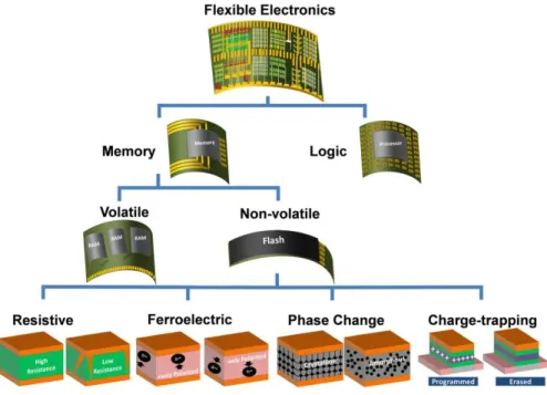
Figure 1.1 Chart representing new NVM memories on flexible substrates. Adapted from[87]. .. 6
Figure 1.2 Illustration of the two possible switching in RRAM. Dashed lines represent the measures where compliance current (CC) take effect. a) MIM configuration. b) Unipolar switching. The set voltage is always higher than the reset voltage and the reset current is always higher than the set current which is limited by the CC. Voltage polarity is non-relevant. c) Bipolar switching. The set operation happens on one polarity of the voltage/current and the reset operation requires the opposite polarity. CC is used as a safe measure. Adapted from[42] ... 7
Figure 1.3 Example of multiple applications using nanoparticles based inks to produce electronic devices on flexible substrates. Adapted from [88]. ... 8
Figure 3.1 Topographical view, obtained by SEM, of NPs synthetized using triton X-100 as surfactant and glucose as reducer. ... 13
Figure 3.2 Topographical view of NPs synthetized using glucose, obtained by SEM. a) Truncated octahedral NPs with sizes around 600nm. In this synthesis 3.5mL of acid oleic were used as surfactant. b) Some NPs present a dodecahedral shape with sizes around 200nm. The only difference to sample a) was an increase on acid oleic to 5mL. ... 14
Figure 3.3 Topographical view, obtained by SEM, of NPs synthetized using acid ascorbic as reducer. ... 14
Figure 3.4 a) NPs synthetized without surfactant (PVP). b) NPs synthetized using PVP 10K molecular weight. ... 16
Figure 3.5 SEM topographical view of the synthetized Cu2O NPs and respective XRD diffractogram. ... 17
Figure 3.6 Evidence of semiconductor behavior exhibited by the Cu2O NPs. ... 17
Figure 3.7 TG-DSC curves from the synthetized Cu2O NPs. ... 18
Figure 3.8 XRD diffractograms of the study focused on the thermal stability of the NPs. ... 19
Figure 3.9 XRD diffractograms of the samples stored in: a) eppendorfs; b) vacuum; to a total of 8 weeks. ... 20
Figure 3.10 DSC-TG curves of the solvents used to disperse the NPs. ... 21
Figure 3.11 ATR-FTIR spectra, at room temperature, of the used solvents to disperse the NPs. ... 21
Figure 3.12 ATR-FTIR spectra of the used solvents to disperse the NPs, when submitted to increased temperatures. ... 22
Figure 3.13 XRD diffractograms of the formulated ink when submitted to different annealing temperatures. ... 23
Figure 3.14 Typical I-V characteristics from 5 cycles performed on a device produced on glass substrate, showing a unipolar switching. In its virgin state, the device was in an HRS. .... 24
Figure 3.15 Typical retention characteristics of the produced device under a Vread =0.3V. ... 25
Figure 3.16 a) I-V characteristics obtained from a device using only ethylene glycol as insulator in a MIM structure. b) Respective retention characteristics at Vread=0.3V. ... 26
Figure 3.17 Typical I-V characteristics of a device produced on paper substrate, using the new formulated ink, also showing unipolar switching. In its virgin state the device was found to be in LRS. ... 26
Figure 3.18 Paper device retention characteristics up to: a) 10 seconds (measured retention during cyles); b)10 000 seconds; showing an ON/OFF current of approximately 104 for a Vread=0.3V. ... 27
Figure 3.19 SEM cross-section topographical view of the active layer in: a) glass substrate device; b) paper substrate device. ... 28
CU2O NANOPARTICLES FOR APLICATION IN PRINTED AND FLEXIBLE ELECTRONICS XVI Figure 3.21 Backside of samples of the initial ink composition containing glycerol, when
submitted to 300ºC in a hotplate. ... 30
Figure 3.22 Backside of the sample: a) containing ethylene glycol as solvent; b) containing glycerol as solvent. ... 30
Figure 3.23 XRD diffractograms for samples containing: a) ethylene glycol; b) glycerol. ... 31
Figure 3.24 Backside of the samples using: a) initial ink solvents; b) only glycerol as solvent. NPs used were synthetized without PVP. ... 31
Figure 3.25 I-V curves of the conductive films when using: a) 10min ramp; b) 20min ramp. ... 32
Figure 6.1 Color cycle during synthesis process. ... 46
Figure 6.2 Topographical SEM Images of the NPs synthetized during the study in table 3.1. All images were taken using the same zoom magnitude except D1 and D3, were half the magnitude was used. ... 48
Figure 6.3 ATR-FTIR spectra of glycerol. ... 49
Figure 6.4 ATR-FTIR spectra of ethylene glycol. ... 49
Figure 6.5 Viscosity results for the initially prepared ink. ... 50
Figure 6.6 Viscosity results of the ink optimized for memory devices. ... 51
Figure 6.7 Typical I-V characteristics of a device annealed above 100ºC. Considered short-circuited. ... 52
CU2O NANOPARTICLES FOR APLICATION IN PRINTED AND FLEXIBLE ELECTRONICS 1
MOTIVATION
In the present day, technological advances have proportioned a better life style for the global population. As individuals in our daily basis electronic needs (e.g. smartphones, pc, tablets), but also in scientific areas of general interest (e.g. the SpaceX program which is probably the one that got more public attention in these last years). That way it opened new opportunities which come with some drawbacks. The rapid technological advances have led to a significant decrease in the lifetime of consumer electronics and therefore an increase in electronic waste as well a rapid consumption of non-renewable resources[1], [2]. To minimize these problems, new devices using biodegradable and non-toxic materials on flexible substrates are emerging every year[3]. It is expected that the revenue of flexible electronics could reach 30 billion USD by 2017 and over 300 billion USD in 2028[4].
Paper substrates is being explored as an alternative to conventional substrates and are getting popular among these new “green devices” as they are degradable, cheap, flexible, eco-friendly and renewable[5]–[7]. Although, researchers are still struggling to archive the same high performance and reliability that we are used to, hoping that one day this green technology will be part of our quotidian.
Another problem associated with today´s electronic devices is their production methods. They are fabricated using specific deposition methods such as lithography, chemical vapor deposition and sputtering, that require a specific environment (dust free and controlled temperature) which is expensive to maintain. The “green technology” is also associated with cheaper and less demanding printing techniques. Solution based techniques are a good alternative as they only require a preparation of nanoparticles ink. In this perspective inkjet printing[8] is found to be a popular method due to its easy control by PC software, but there are other options such as screen-printing[9], and pen writing. This last one is gaining popularity since is found to be a simpler, rapid, low cost and user-friendly compared to the other methods. It simply requires a refillable pen and small size NP´s ink to avoid blocking the printing tip[10]. The aim of this work is to produce cuprous oxide (Cu2O) nanoparticles (NPs) and include
them as part of electronic devices, using cost-effective and biodegradable materials through simple and inexpensive methods. A study on the NPs synthesis will be conducted to achieve NPs sizes compatible with pen-writing method. Inks including a mixture of NPs and organic compounds such as ethylene-glycol and absolute ethanol will be used to print the insulator layer in metal-insulator-metal (MIM) devices, in which the metal contacts are from gold deposited by e-beam evaporation, and study their applicability towards resistive switching RAMs (RRAM) on paper substrates. Also, inks with NPs dispersed in mainly glycerol were drop-casted on glass substrates to produce copper (Cu) films when annealing at around 300 (ºC) degrees Celsius.
In short, the focus is to synthetize Cu2O and study their applicability on RRAM devices
CU2O NANOPARTICLES FOR APLICATION IN PRINTED AND FLEXIBLE ELECTRONICS 3
OBJECTIVES
The main objective of this thesis is the synthesis of cuprous oxide nanoparticles (NPs) through simple methods and non-toxic reagents, for application in flexible electronic devices. For this reason, the chosen method was liquid-phase synthesis, and the reducer reagents glucose and ascorbic acid. Then an ink containing the NPs and compatible with pen-writing printing should be elaborated, where layers containing the NPs will be printed on paper as part of electronic devices.
Therefore the following themes will be covered:
• Study of Cu2O NPs synthesis and respective morphology and stability.
• Ink formulation and characterization.
• Electrical characterization of RRAM devices fabricated on glass and paper.
CU2O NANOPARTICLES FOR APLICATION IN PRINTED AND FLEXIBLE ELECTRONICS 5
1
Introduction
It will be presented a brief introduction on the relevant topics to better understand the following chapters. This introduction consists in three sections. An explanation on the p-type behavior of cuprous oxide and an approach on their synthesis with special attention to liquid phase synthesis. Followed by a view on the non-volatile memories with emphasis in RRAM devices, and finally an overview about nanoparticles based inks and their requisites to be compatible with pen-writing method.
Copper Oxide type-I (Cu
2O)
Cuprous oxide (Cu2O), also known as “cuprite” is one of the oldest materials of
semiconductor electronics and it generally appears as a red colored solid. It is low cost, nontoxic, abundant, has a high solar spectral absorption coefficient and special energy-band configuration[11] making it suitable for application such as photovoltaic devices[12], gas sensing[13], memory devices[14] and lithium-ion batteries[15].
1.1.1
Atomic structure, electronic properties and p-type behavior
Cu2O has an unusual structure, it crystalizes in a simple cubic structure that can be
observed as two sublattices: a face-centered cubic (fcc) sublattice of cooper cations and a body-centered cubic (bcc) sublattice of oxygen anions. Besides cuprite, only Ag2O and Pb2O have this
crystal structure for the actual metal oxides[16].
It is known that cuprite is an intrinsically p-type semiconductor (holes conduction), with a bulk band gap of 2.0-2.17 eV[17]–[19]. Cu2O is intrinsically copper deficient due to formation
of copper vacancies VCu that act as a shallow and efficient hole producers, as showed by
Raebiger et al.[20]. To justify this behavior, they reported that Cu2O is intrinsically a p-type
semiconductor because the potential hole killer VO has no transition level in the gap and thus
cannot annihilate holes, and the possible hole killer Cu16 has both high formation energy and
deep transition level and is thus incapable to efficiently destroy holes created by VCu.
Simplified, it is believed that VCu are the cause of the p-type semiconductor character of Cu2O.
Although, it can also present a n-type character when the density of oxygen vacancies is higher than that of copper vacancies[19].
1.1.2
Synthesis
Normally Cu2O is obtained either via oxidation of pure copper (thermal oxidation) or via
reduction of Cu2+. Referring to the second method, in literature, there are several reports using
different methods for the synthesis of Cu2O nanoparticles/films such as electrochemical
deposition[21], microwave[22], solvothermal methods[23], liquid phase synthesis[24]–[28], seed-mediated synthesis[29] and microemulsions[30]. All these were used to archive Cu2O
nanoparticles with different sizes and morphologies and in certain methods even control these parameters.
From all these methods, there is a need to highlight liquid phase synthesis, as they are simple to execute, do not require expensive lab gear, or handling of hazard reagents, are low cost and less time consuming. In this method, most synthesis generally starts with the addition of sodium hydroxide to a copper salt (e.g. copper chloride, copper acetate, copper nitrate, or copper sulfate)[31], and then a reducer agent such as acid ascorbic or glucose is added to obtain Cu2O nanoparticles. To note that in case of using glucose temperature is needed for the reaction
CU2O NANOPARTICLES FOR APLICATION IN PRINTED AND FLEXIBLE ELECTRONICS 6
Memories
The ideal non-volatile data memory (NVM) should have characteristics such as fast write and read access, low energy operation, high-density and low cost, and high performance relating to endurance and retention time[36].
1.2.1
Memory technologies
Nowadays, Flash memory devices standout in the NVM category due to high density and low fabrication cost. However, they suffer from low endurance, low write speed, and high voltages are required for the write operations. Another problem is that Flash memories are soon expected to run into physical limits with the increase density[37], [38].
Alternative memory concepts are emerging such as Magnetoresistive random access memory (MRAM)[39] and Ferroelectric RAM (Fe-RAM)[40], in which a magnetic field is evolved in the resistance switching, and Phase-change RAM (PC-RAM)[41], in which thermal processes control a phase transition in the switching material from the amorphous to the crystalline state. But this memories exhibit technological and inherent problems in the scalability, as they cannot achieve the same density as Flash memories today. To surpass the problems of these NVM concepts, another concept is being explored which is based on the electrically switchable resistance of a metal-insulator-metal (MIM) memory device usually called Resistance switching RAM (RRAM)[42]. The “M” in MIM refers to a good electron
conductor, and it can differ on the two sides, while the “I” refers to insulator, often an ion-conductor material. A common benefit to previously mentioned concepts is their compatibility with flexible substrates (figure 1.1).
Figure 1.1 Chart representing new NVM memories on flexible substrates.
CU2O NANOPARTICLES FOR APLICATION IN PRINTED AND FLEXIBLE ELECTRONICS 7
1.2.2
RRAM
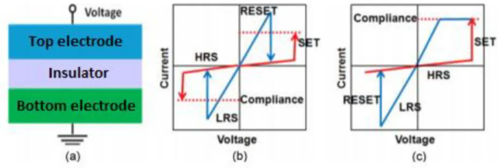
In RRAM memory types, generally an initial electroforming step such as a current-limited electric breakdown is applied in the prepared sample. This step preconditions the system which can subsequently be switched between a conductive (ON) state and a less conductive (OFF) state. There are two different switching types in RRAM: unipolar, also known as symmetric since normally both electrodes are made up from the same material; and bipolar, known as antisymmetric due to use of different materials for each electrode. In a detailed explanation, switching is called unipolar when the switching procedure is independent from the polarity of the voltage and current signal. To change the system from its high-resistance state (OFF) to the low-resistance (ON) state, a threshold voltage needs to be applied, as shown in figure 1.2. This process is called “set”, and the current is limited by the compliance current set in the control circuit. To “reset” into the OFF state a higher current and a voltage bellow the set
voltage is applied. On the contrary, the switching is bipolar when the set to an ON state occurs at one voltage polarity and the reset to the OFF state on reversed voltage polarity, as illustrated in figure 1.2c. In both cases, the reading of the state is conducted at low voltages incapable of switching the memory state[43].
Figure 1.2 Illustration of the two possible switching in RRAM. Dashed lines represent
the measures where compliance current (CC) take effect. a) MIM configuration. b)
Unipolar switching. The set voltage is always higher than the reset voltage and the reset current is always higher than the set current which is limited by the CC. Voltage polarity is non-relevant. c) Bipolar switching. The set operation happens on one polarity of the
voltage/current and the reset operation requires the opposite polarity. CC is used as a safe measure. Adapted from[42]
1.2.3
Organic and inorganic RRAM
The first reports of such resistive switching phenomena date back to the 1960s when Hickmott reported the use of oxide insulators in MIM configuration[44]. Since then multiple materials have been reported to show hysteric resistance switching, such as binary and multinary oxides and as well organic compounds.
CU2O NANOPARTICLES FOR APLICATION IN PRINTED AND FLEXIBLE ELECTRONICS 8 When using organic compounds for the insulator layer, charge trapping seems to be the most common mechanism[48]–[50]. Structural disorder in amorphous organic thin films can result in the presence of localized electronics states which can trap and store charge in equilibrium leading to a low-resistive state (ON state)[51], [52]. The presence of such trapped charges can dominate the current-voltage (I-V) characteristics of organic devices due to relatively low density of intrinsic free charge carriers in organic solids[53]. Freeing the charges returns to the OFF state, it could be either by applying a reverse voltage or a higher current.
Hybrid memories are also possible, as there are reports where metal oxide nanoparticles help in the charge trapping mechanism of organic memories, acting as a stabilizer[49], [50]. Others cases report NPs filament formation in an organic matrix[54].
1.2.4
Memories on flexible substrates
As technology advances, the demand for thin and lightweight devices increases to develop large area electronics such as sensors[55]–[58], displays[59] and actuators[60]. Flexible NVM have attracted a lot of attentions for data storage in future electronics applications. They include characteristics as thin, lightweight, printable, foldable and stretchable which are very attractive advantages from device perspective. Flexible memories are part of the next generation devices like smartphones, TV´s and others consumer electronics, since they are the fundamental component of all modern electronic system to act as code storage, data storage, static and dynamic memory. In the last few years, a considerable amount of research work is being focused towards memories on flexible substrates[61]–[64] (e.g. paper, polymeric), to investigate their performance[65].
Nanoparticles based inks
The inks must meet strict physicochemical properties such as viscosity, surface tension and adhesion to a substrate to archive optimal performance and reliability of the printing system and to obtain the best printed pattern[66]. Most inks used today in personal or office printers are water-based inks, which are composed by many components (binders, humectants, wetting and dispersing agents, buffer components, chelating agents, defoamers, biocides, etc.) optimized to meet the complex requirements for good printing performance.
1.3.1
Ink composition
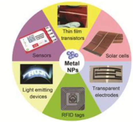
In the last decades, many applications using nanoparticles ink emerged (figure 1.3), such as fabrication of organic light-emitting diodes[67], transistors[68], integrated circuits[69] and conducting lines[70], [71].
CU2O NANOPARTICLES FOR APLICATION IN PRINTED AND FLEXIBLE ELECTRONICS 9 New approaches are required for preparation of inks containing functional materials, which may be of organic and/or inorganic origin. These materials may be either soluble (dye-like) or insoluble (pigment-(dye-like), so the ink is either a solution or a dispersion. Nanoparticles inks are considered dispersions which contain nanoparticles in the size range of a few hundred nanometers. In case of using ink-jet or the pen writing method, reducing the particle size to 50 nanometers or less is a requirement to archive reliability, otherwise the printing head can clog. They can be dispersed in water, oils, or organic compounds as the target is to get a good homogenization[72]. Although, viscosity should be kept in a controlled range depending on the specification of the printing technique (e.g. the pen used in his work between 1 cP and 20 cP).
1.3.2
Printing techniques on flexible substrates
Some of todays most used printing techniques on flexible substrates are inkjet, screen-printing and pen-writing. Inkjet screen-printing is the most popular, as in can be controlled by PC software and used for a variety of substrates, nevertheless it requires a proper equipment which can be in some cases expensive[70]. Screen-printing technique has the requirement of high viscosity which may not be suitable for some applications, (e.g. in this work ethylene glycol/ethanol is used as dispersing agent which has a low-medium viscosity, around 12 cP). That said, pen-writing seems to be the most suitable method. It works well on paper substrates,
CU2O NANOPARTICLES FOR APLICATION IN PRINTED AND FLEXIBLE ELECTRONICS 11
2
Materials and Methods
In this chapter, will be explained how to synthetize Cu2O NPs, followed by the ink
formulation for pen-writing and drop-casting. Then a description of the methods used, and finally an insight on how the memories and the conductive films were characterized. Supportive information can be found in annex A.
Materials and reagents
Polyvinylpyrrolidone powder (PVP, MW ~40000, CAS:9003-39-8) and copper (II)
chloride powder (CuCl2 ≥99.995%, CAS:7447-39-4) purchased from Sigma-Aldrich, sodium
hydroxide Eka PelletsTM (NaOH, CAS:1310-73-2) from AkzoNobel, and ascorbic acid (vitamin
C ≥99.8%, CAS:50-81-7) from Absolve.
Synthesis of Cu
2O
The procedure to liquid phase synthetize Cu2O NPs was adapted from [79].
In a typical procedure at RT, 10.0 mL NaOH aqueous solution (2.0 mol/L) was added dropwise into 100 mL CuCl2 aqueous solution (0.01 mol/L) containing 2.22g PVP. After stirring
at 300 rpm for 30 minutes, 10.0 mL ascorbic acid solution (0.6 mol/L) was added dropwise into the solution. The mixed solution was stirred for 1 minute until it turns into an opaque orange solution. To collect the NPs the solution was centrifuged for 15 minutes at 4000 rpm, and then the precipitate was washed three times with distilled water and one with absolute ethanol in the same conditions of the initial centrifugation. Finally, it was dried in vacuum at 60ºC for 5 hours.
Ink formulation
This work involves the preparation of two different inks, one for memory devices and other for conductive films.
The first one was prepared by dispersing 0.4g of Cu2O NPs in 1mL of mixed ethylene
glycol and ethanol at a ratio of 50/50 vol% (28.6wt%). Followed by sonication using a Sonics Vibracell VC505 with a 630-0421 coupler and a 3.0mm 630-0418 tip with 30s/30s (on/off) pulses, at 40% amplitude during 5 minutes.
In the second one, 0.4g Cu2O NPs was dispersed in 1mL glycerol (28.6%) and sonicated
in the same conditions during 10 minutes.
Memory fabrication
All the memory devices were fabricated using the same architecture: Glass; Paper/Au/Cu2O Ink/Au. The figure 2.1 represents a basic schematic of the fabricated RRAM
devices.
The bottom common contact consists of a 60nm layer of Au deposited by e-beam evaporation.
The active layer was deposited using two methods. On paper, using a refillable parallel pen FP3 6.0 mm purchased from Pilot, with some single passages in all the device´s area. For glass substrate, spin-coating was the chosen method, with 2000 rpm during 30 seconds. Kapton tape was previously used to cover a corner to guarantee access to the bottom contact. Then the device was submitted to a cure during 1h at 100ºC in a hotplate to dry the ink and evaporate the ethanol.
CU2O NANOPARTICLES FOR APLICATION IN PRINTED AND FLEXIBLE ELECTRONICS 12 of a 7x7 matrix compromised square contacts, whose area varies from line to line as illustrated in figure 2.1. The studied areas were: 0.5mm2, 0.75mm2, 1mm2, 1.25mm2, 1.5mm2, 1.75mm2
and 2mm2.
Figure 2.1 Schematic representation of the fabricated RRAM devices.
Conductive films fabrication
The conductive films/lines were prepared by simply drop-casting the Cu2O ink on
patterned glass substrates. The pattern was previously made using kapton tape. After an annealing at 300ºC during 1h in an oven, the tape was carefully removed leaving Cu lines matching the desired pattern.
Characterization
Several characterization techniques were used to confirm the presence of Cu2O NPs, their
stability, as well to characterize the RRAM devices and the conductive films.
The crystallinity and structure of synthetized Cu2O NPs was confirmed using X-Ray
Diffraction (XRD, PANalytical, model X´Pert Pro), in Bragg-Brentano geometry with Cu Kα
line radiation (λ=1.5406 Å) at 45 KV and 40 mA. XRD was also used to study their air/vacuum stability and thermal degradation. To complement the thermal degradation study thermogravimetric and differential scanning calorimetry (TG-DSC) measurements were carried out with a Simultaneous Thermal Analyzer (TG-DSC – STA 449 F3 Jupiter). NPs morphology were characterized by scanning electron microscopy (SEM) and energy dispersive spectroscopy (EDS) using a Carl Zeiss Auriga crossbeam (SEM-FIB) workstation instrument equipped with an Oxford X-Ray energy dispersive spectrometer. Nanoparticles semiconductivity was characterized using a BIO RAD cryostat system coupled with a Keithley 617.
To study the inks thermal degradation Fourier Transform Infrared (FTIR) spectroscopy was performed using a Nicolet 6700 FTIR Thermo Electron Corporation device in complementation with TG-DSC analysis. Ink viscosity was measured using a Brookfield CAP +2000 viscometer.
Morphological characterization of the RRAM devices was carried out using SEM and EDS techniques. All electrical characterizations were performed on a Keysight B1500A semiconductor parameter analyzer apart from vacuum electrical characterization, which was performed on a Keithley 4200-SCS semiconductor parameter analyzer connected to a Janis ST-500 probe station. All I-V characterizations were performed using a 20mV step and 250ms sweep delay. No hold time was used in any case. Other parameters such as retention time and compliance current (CC) are described in the result section, since they are custom.
CU2O NANOPARTICLES FOR APLICATION IN PRINTED AND FLEXIBLE ELECTRONICS 13
3
Results
This section will be split into four topics, beginning with a study made on the Cu2O
synthesis and on how the best method was chosen and why, and the respective NPs characterization. Then a topic including the characterization of the ink. In third, will be presented memory devices based one the synthetized NPs and their characterization, as well an insight on the possible memory mechanism. The final part will be about the conductive films that appear when the synthetized NPs are dispersed in specific solvents and annealed at temperatures around 300ºC, and a possible explanation for this event.
Cu
2O nanoparticles synthesis
3.1.1
Synthesis parameters study
On this work the synthetized NPs will be integrated on ink compatible with the pen writing printing method. One of the requirements is to use inks where NPs are small enough to avoid blocking the printing tip, therefore the focus of the presented study. Note that the required maximum size will depend on the chosen pen. Besides that, cheaper and easily synthesis will be prioritized to produce the NPs.
As according to the introduction, most articles found in the literature for liquid phase synthesis of Cu2O use either glucose or ascorbic acid as reducer. On both cases there are reports
synthetizing NPs with sizes under 100nm, which is believed to be small enough since in this work is used a parallel pen. If we assume that the same size can be achieved using any of the reducers, then the priority is to the cheaper one, which is glucose.
A typical procedure was used[35], in which Cu2O nanosized particles had been reported,
and the results obtained by Scanning Electron Microscopy (SEM) can be seen in figure 3.1.
Figure 3.1 Topographical view, obtained by SEM, of NPs synthetized using triton X-100
as surfactant and glucose as reducer.
CU2O NANOPARTICLES FOR APLICATION IN PRINTED AND FLEXIBLE ELECTRONICS 14 Following these results other synthesis using glucose were experimented, using different procedures including variations in temperature, concentration and used surfactants[32].
Figure 3.2 Topographical view of NPs synthetized using glucose, obtained by SEM. a)
Truncated octahedral NPs with sizes around 600nm. In this synthesis 3.5mL of acid oleic were used as surfactant. b) Some NPs present a dodecahedral shape with sizes around
200nm. The only difference to sample a) was an increase on acid oleic to 5mL.
In figure 3.2 we can observe the results and it is clear that these synthesis result in smaller particles. At the left, figure 3.2 a), the truncated octahedral shape is consistent as well the size of the particles, and they are smaller than those before as expected per the followed procedure. Since consistent results with the report were achieved, it was decided to increase the surfactant concentration to achieve even smaller NPs. On the right, figure 3.2 b), we can see the results and although the non-uniformity where some particles present a dodecahedral shape, smaller NPs are visible. Higher reaction times are expected to uniformize the size and shape but has the downside of increasing particles size as predicted by the Ostwald ripening[80].
These particles are smaller but not small enough to be compatible with the pen writing method. For that reason, it was decided to try synthesis using ascorbic acid as reducer to compare the differences and try to achieve even smaller NPs.
The followed procedure is described in the materials and methods section, which is adapted from [79] with a reduction in the reaction time, expecting that way to obtain smaller NPs than synthetized by the author with sizes above 400nm. Figure 3.3 shows the result, confirming the expected.
Figure 3.3 Topographical view, obtained by SEM, of NPs synthetized using acid
CU2O NANOPARTICLES FOR APLICATION IN PRINTED AND FLEXIBLE ELECTRONICS 15 The obtained NPs present an irregular round shape with a narrow size distribution visually centered around the 68 ± 20 nm. Furthermore, these sizes are compatible with the used parallel pen as will be shown ahead in this section. The fact that the NPs do not present any specific shape is due reduced reaction time, since is the only different to the original procedure where synthetized NPs presented a well-defined shape. Also, the small deviations in size, mostly smaller NPs can be explained by the Ostwald ripening due the reduced reaction time.[80]
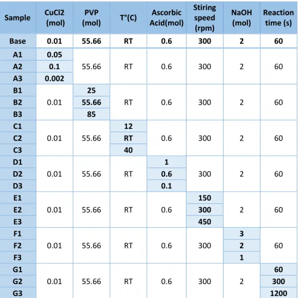
In order to understand the influence of each reaction parameter in the final size of NPs, a study was made considering the parameters listed in table 3.1.
Table 3.1 Studied parameters on the final morphology of the NPs synthetized using acid
ascorbic as reducer.
Sample CuCl2 (mol)
PVP
(mol) T°(C)
Ascorbic Acid(mol) Stiring speed (rpm) NaOH (mol) Reaction time (s)
Base 0.01 55.66 RT 0.6 300 2 60
A1 0.05
55.66 RT 0.6 300 2 60
A2 0.1 A3 0.002 B1
0.01
25
RT 0.6 300 2 60
B2 55.66
B3 85
C1
0.01 55.66
12
0.6 300 2 60
C2 RT
C3 40
D1
0.01 55.66 RT
1
300 2 60
D2 0.6
D3 0.1
E1
0.01 55.66 RT 0.6
150
2 60
E2 300
E3 450
F1
0.01 55.66 RT 0.6 300
3
60
F2 2
F3 1
G1
0.01 55.66 RT 0.6 300 2
60
G2 300
G3 1200
The respective SEM images are part of annex B where is possible to see the synthetized NPs according to the presented table. The discussed results will always be relative to the “base”
CU2O NANOPARTICLES FOR APLICATION IN PRINTED AND FLEXIBLE ELECTRONICS 16 higher concentrations no significant difference is observed. This shows that the solution is most likely saturated with surfactant and there is no point in going further with higher amounts of surfactant. Temperature influence is expected to create larger NPs with higher temperatures and vice-versa. In an ice bath synthesis, SEM image does not show a significant reduction in NPs size although it seems to present a better uniformity which is a positive point but requires an additional step in the procedure, which given the results do not seem to be a crucial improvement. When applying temperature, NPs are not substantial bigger but the non-uniformity is more significant with some NPs presenting an elongated shape. Next is the reducer concentration influence, where results show that when using 1 mol of ascorbic acid NPs increase in size and tend to present an octahedral shape. This could be explained due to faster aging of NPs since it is expected that higher amounts of reducer produce more NPs assuming it is not the limitation factor. When using 0.1 mol there is no change in size but it is visible than the reaction produced less powder. Lowering the stirring speed to 150 rpm does not show any major improvement in NPs size, and only the non-uniformity in this case seem to increase among the NPs size. For 450 rpm the uniformity seems consistent with the base sample but NPs tend to present larger sizes which can be explained by the accelerated ageing of the process. For sample F1, higher concentrations of NaOH NPs tend to aggregate and form larger NPs and it is visible a significant increase in the non-uniformity of sizes. In F3, the lower concentration resulted in smaller NPs but also in a reduced quantity of powder making it not a viable production. The study on the reaction time is only present as a complement as it is expected to increase NPs size. That is demonstrated in sample G2 and G3. Lower reaction times were not tested since 60 seconds was found to be the minimum required time for the solution turn opaque orange.
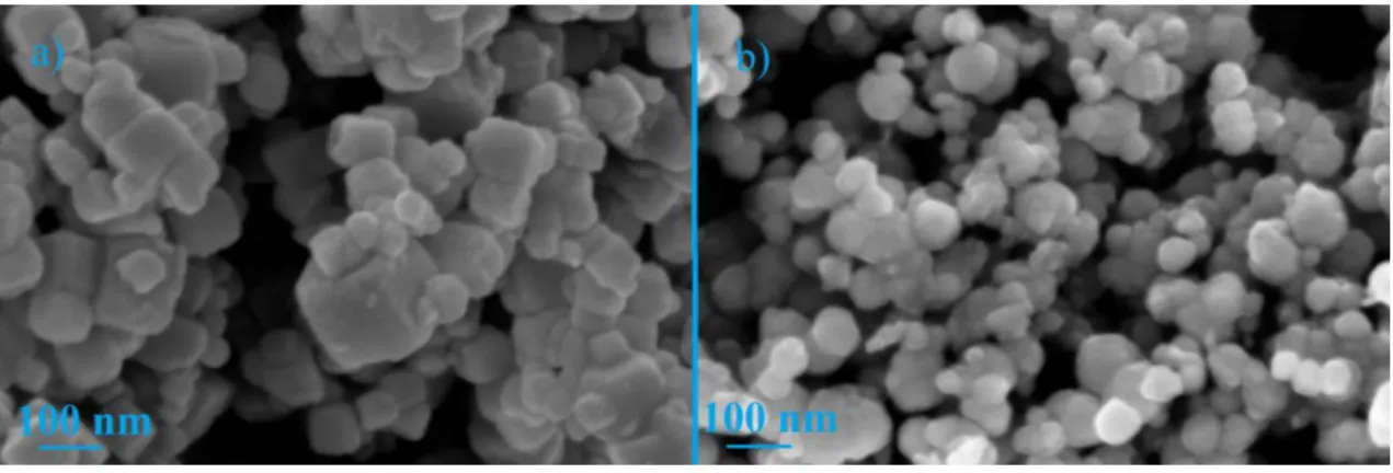
To complement the influence of the surfactant in this synthesis two more tests were carried out, one with no PVP and other with 10K PVP to spot the differences (figure 3.4).
Figure 3.4 a) NPs synthetized without surfactant (PVP). b) NPs synthetized using PVP 10K
molecular weight.
On the left, figure 3.4 a) where no PVP was used, it is observed bigger NPs as expected with the tendency to form cubes which match the cubic lattice from Cu2O. The formed cubes
present non-uniform sizes since NPs are still in the agglomeration process. Although, the small NPs formed in the absence of a surfactant, mean that the high dilution of the precursors act also as a parameter to achieve small NPs. On the right, figure 3.4 b), it is possible to observe that the NPs synthetized using PVP 10K present worst uniformity since sizes range from 60nm to 100nm, when compared to the ones using PVP 40K. This means that the molecular weight of the chosen surfactant is also a parameter that can influence the NPs size.
CU2O NANOPARTICLES FOR APLICATION IN PRINTED AND FLEXIBLE ELECTRONICS 17 simple lab materials required and non-complex procedures were part of the screening of the chosen procedures.
3.1.2
Characterization
From now forward, all references to the Cu2O NPs will always be to the ones synthetized
with the procedure chosen before (base).
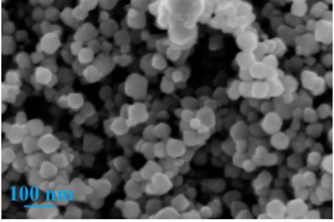
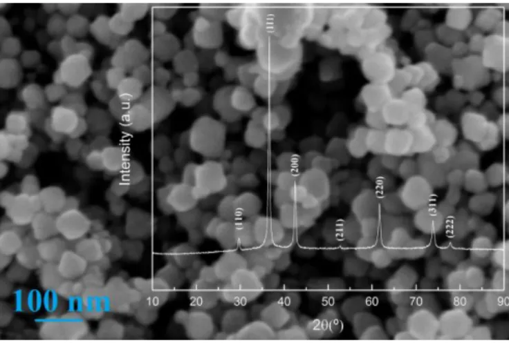
Figure 3.5 SEM topographical view of the synthetized Cu2O NPs and respective XRD
diffractogram.
In figure 3.5, SEM image shows that NPs present non-uniform sizes around 65nm with a round non-defined shape. The synthetized NPs X-RAY Diffraction (XRD) peaks match with Cu2O with cubic structure (lattice constant a = b = c = 4.2696 Å) according to ICDD
00-005-0667, confirming its presence.
Cuprous oxide, is known as a semiconductor, and to prove that an experiment was carried out where the resistivity was studied based of the variation of temperature. The sample was prepared in a paper substrate that had previously gold contacts deposited by e-beam, then the NPs that were temporarily dispersed in Isopropyl Alcohol (IPA) were drop-casted onto the paper which was left to dry on a hotplate at 60ºC during 20 minutes. The results from the resistivity test carried out in the cryostat can be seen in figure 3.6.
Figure 3.6 Resistivity dependency of temperature variation. Demonstrating the
CU2O NANOPARTICLES FOR APLICATION IN PRINTED AND FLEXIBLE ELECTRONICS 18 The measurements in the figure above ocured in two diferent directions, firstly during the heat up and then during the cooling of the sample. In both cases the temperature step was 5ºC and between each measurement 5 minutes of wait time to stabilize the measured resistance value. Results are consistent with expected semiconductor behavior of the NPs as resistance significantly drops as temperature increases.
3.1.3
Stability
The NPs are intended to be submitted to temperature as part of the possible annealing processes which are a common process during the fabrication of electronic devices. For that reason, the stability of the NPs was studied through thermogravimetric and differential scanning calorimetry (DSC-TG) complemented with XRD.
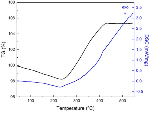
Figure 3.7 TG-DSC curves from the synthetized Cu2O NPs.
Figure 3.7 represent the results obtained from DSC-TG, from 228ºC to 420ºC a mass increase is visible along with an endothermic reaction. This change is associated with the oxidation process of the NPs of Cu2O to cupric oxide (CuO), as new bonds are created. To
CU2O NANOPARTICLES FOR APLICATION IN PRINTED AND FLEXIBLE ELECTRONICS 19
Figure 3.8 XRD diffractograms of the study focused on the thermal stability of the NPs.
The results from XRD are presented in figure 3.8 and corroborate the results obtained in DSC-TG. From RT to 150ºC clear peaks of Cu2O are visible, then at 200ºC the peaks start to
decrease and at 250ºC is clearly visible a shifting in the peaks. From 300ºC to 500ºC CuO peaks are established and is notable an increase in their intensity as temperature increases, since the presence of CuO also increases. These peaks partially match with CuO with monoclinic structure (lattice constant a = 4.6883 Å, b = 3.4229 Å, c = 5.1319 Å) according to ICDD 00-048-1548.
With this, thermal study revealed that NPs should not be submitted to temperatures above 200ºC in order to maintain the Cu2O phase as a majority.
CU2O NANOPARTICLES FOR APLICATION IN PRINTED AND FLEXIBLE ELECTRONICS 20
Figure 3.9 XRD diffractograms of the samples stored in: a) eppendorfs; b) vacuum; to
a total of 8 weeks.
Starting with the samples stored in vacuum, no oxidation is observed throughout 8 weeks. Since there is no exposure to atmosphere, or more precisely to oxygen the oxidation process is minimal or non-existent. For the samples stored in eppendorfs there is no signs of oxidation during the first 3 weeks, but they start to appear at the fifth week. From week 6 to week 8 is clearly visible the shifting of peaks, although Cu2O peaks remain present and more intense than
the new formed ones, indicating that is present a mixture of CuO and Cu2O being this last state
the majority. Resuming NPs can be stored plus 8 weeks in vacuum and until 3 in eppendorfs.
Ink formulation and characterization
For application in pen-writing the NPs need to be dispersed is some sort of liquid, either it is water, an alcohol, some type of organic compound or even a mixture of some of the mentioned. After multiple tries using only water or ethanol and a mixture of both, 24h agitations, ultrasounds and sonications without success, the need to use organic compounds urged. They can easily the process of dispersing the NPs as they can act as a binder in conjunction with the PVP adsorbed on the surface of the NPs which act as a dispersant, but also bring the need to use higher annealing temperatures to remove or partially degrade the solvent. Later on this section will be explained how part of the solvents play a role in both approached applications, removing the need to remove or degrade the solvents. But first, the path to those findings will be explained.
CU2O NANOPARTICLES FOR APLICATION IN PRINTED AND FLEXIBLE ELECTRONICS 21
Figure 3.10 DSC-TG curves of the solvents used to disperse the NPs.
The results for DSC-TG, in figure 3.10, shows a decrease in mass till approximately 210ºC, with a loss of 89.79% of the initial mass. For higher temperatures the mass change is despicable, so in order to maximize the solvents degradation annealing temperatures around 210ºC are required. It is also possible to seem fout endothermic peaks before 200ºC which are associated with the evaporation of the 4 solvents. Checking the boiling points of each solvent it is known that the first to evaporate will be ethanol, followed by water, then ethylene glycol and finally glycerol, so respectively the correspondent endothermic peaks are at 66ºC[82], 102ºC[83], 144ºC[84] and 205ºC[85].
To complement the results and better understand the degradation of the solvents, FTIR spectroscopy was performed. Figure 3.11 shows the ink spectrum at RT. Since both water and ethanol evaporate at relatively low temperatures, the focus will be the spectrum of glycerol and ethylene glycol which can be found in annex C.
Figure 3.11 ATR-FTIR spectra, at room temperature, of the used solvents to disperse the
CU2O NANOPARTICLES FOR APLICATION IN PRINTED AND FLEXIBLE ELECTRONICS 22 For study purposes the ink was submitted to four different temperatures: 140ºC, 160ºC, 180ºC and 200ºC. The steps were chosen based on the endothermic peaks observed in DSC-TG and the results can be found in figure 3.12.
Figure 3.12 ATR-FTIR spectra of the used solvents to disperse the NPs, when submitted
to increased temperatures.
FTIR results confirm the endothermic peaks shown by DSC-TG, where the major degradation of the organic solvents happens from 140ºC to 160ºC which is associated with the degradation of ethylene glycol and also part of glycerol since the spectrum differ from the original one of glycerol. The following spectrums represent the degradation of the remaining glycerol. This means that at 160ºC most solvents have evaporated or been severely degraded, which is a positive point since is expected to produce electronic devices using paper substrate that only support annealing temperatures around 150/160ºC.
The next step is to repeat the process but with NPs dispersed in the solvents. For that an ink at 28.8wt% was prepared which resulted in a viscosity of 12.9cP (annex D), suitable for pen writing. DRX was used to confirm that Cu2O NPs are still present when the ink is submitted to
CU2O NANOPARTICLES FOR APLICATION IN PRINTED AND FLEXIBLE ELECTRONICS 23
Figure 3.13 XRD diffractograms of the formulated ink when submitted to different
annealing temperatures.
Figure 3.13 shows the results of annealing treatments at different temperatures. From 50ºC to 150ºC Cu2O peaks match the XRD results, but at 200ºC new peaks start to appear. At
250ºC those new peaks became more intense, matching copper (Cu) peaks with cubic structure (lattice constant a = b = c = 3.6150 Å) according to ICDD 00-004-0836.
This results demonstrate that the maximum annealing temperature should be around 150ºC to avoid changes in the crystallinity of the NPs. Although at 250ºC Cu peaks appear instead of CuO as it would be expected. This result will be approach at the final topic of this section.
Memory devices
3.3.1
Electrical characterization
In this section, will be presented the results for the produced memories using the synthetized NPs. In a first step, memories were produced in glass substrates with annealing treatments varying from 160ºC to 100ºC in 10ºC steps. The devices annealed at 100ºC were the only ones proved to be a working memory, all the others were considered short-circuited. The respective electrical characterization is presented in figure 3.14 and annex E, respectively. All the analyzed results will be using the 2 mm2 top contacts as they had a higher working rate and
CU2O NANOPARTICLES FOR APLICATION IN PRINTED AND FLEXIBLE ELECTRONICS 24
Figure 3.14 Typical I-V characteristics from 5 cycles performed on a device produced on
glass substrate, showing a unipolar switching. In its virgin state, the device was in an HRS.
CU2O NANOPARTICLES FOR APLICATION IN PRINTED AND FLEXIBLE ELECTRONICS 25
Figure 3.15 Typical retention characteristics of the produced device under a Vread =0.3V.
Figure 3.15 shows the retention results for the same previous device. It is able to maintain it state at least 10 seconds with a window between LRS and HRS of approximately 103. This
measurement had the main purpose of verifying the LRS and HRS currents and not the retention characteristic of the device. As observed before, the one cycle presents an offset and although the switching mechanism is still unknown this effect is typical in filament memories which can be formed by the NPs in this case.
The search to understand the switching characteristic of the device, resulted in 3 statements. This behavior could be caused by the NPs, the organic compounds that remain after the annealing at 100ºC, or a cooperation of both mentioned. Previously, the devices annealed at higher temperatures including 160ºC did not show any memory behavior. At this temperature, most of the solvents have evaporated or been degraded leaving only some residues of glycerol. This means that the layer is mainly formed by the NPs and since no memory behavior was observed it is plausible to exclude that the memory effect is exclusively caused by the NPs. The next step is to explore the option that organic compounds can be the cause just by themselves. Given that the 100ºC annealing treatments resulted in devices with memory effect, paper substrates were used from now since the objective was to produce devices in flexible substrates.
CU2O NANOPARTICLES FOR APLICATION IN PRINTED AND FLEXIBLE ELECTRONICS 26
Figure 3.16 a) I-V characteristics obtained from a device using only ethylene glycol as
insulator in a MIM structure. b) Respective retention characteristics at Vread=0.3V.
In the glycerol device no behavior was observed, being the device consider short-circuited. Since glycerol is not known as an electrical conductor this high current can be explained by the possible low thickness of the film. Figure 3.16 a) shows the I-V results of the ethylene glycol device where some kind of behavior is observed. This shows that the device either has some highly unstable type of memory behavior which can be observed in the retention measure (although it is not a memory), or is just simple the breakdown of the layer due high current since initial cycles had higher currents. In this case the device was in a considerer pre-set state. Either way, devices using a layer of ethylene glycol and NPs were produced as mentioned in the materials and methods section. The formulated ink was composed by ethanol, ethylene glycol and 28.6wt% of NPs resulting in a viscosity of 5.4cP (annex D), compatible with used pen.
Figure 3.17 Typical I-V characteristics of a device produced on paper substrate, using
CU2O NANOPARTICLES FOR APLICATION IN PRINTED AND FLEXIBLE ELECTRONICS 27 Electrical characterization of one of those devices is presented is figure 3.17. In this case the initial state of the device is pre-set and therefore, the first step was to reset the device. An initial I-V sweep without CC resulted in a reset process. The next sweep from 0V to 7V using 1mA CC resulted in a set. About 20 subsequent cycles were performed and are presented in the figure 3.17. The device exhibits a memory behavior with unipolar switching for the same reason mentioned before. Operations voltages in this case are lower, ranging from 0V to 7V, which is an improvement. Another positive aspect is that the reset process is well defined in the voltage axis around 1-1.5V, but the same does not happen for the set process since it occurs at random voltages. Although, the last 3 sets happened at around 3.5V, but further cycles are needed to confirm a possible stabilization. Another aspect is that set voltages always take place at higher voltages than the reset which shows an improvement in stability when compared to the device in figure 3.14. About the endurance it is possible to say that has been improved, where at least 20 cycles were performed but a higher number is required to demonstrate a high endurance. LRS currents are also high (up to mA) and can compromise the endurance of the device for longer cycles.
Figure 3.18 Paper device retention characteristics up to: a) 10 seconds (measured
retention during cyles); b)10 000 seconds; showing an ON/OFF current of approximately
104 for a V
read=0.3V.
CU2O NANOPARTICLES FOR APLICATION IN PRINTED AND FLEXIBLE ELECTRONICS 28
3.3.2
Morphologic characterization
Another aspect to take in consideration and that can also influence the results is the thickness of the active layer. It is expected that the working voltages of the device tend to increase directly with the thickness of the active layer.
Figure 3.19 SEM cross-section topographical view of the active layer in: a) glass
substrate device; b) paper substrate device.
In figure 3.19 we can see the thickness of both active layers, where on glass has approximately 3.5-3.75 µm and on paper 2-2.5 µm. Although, just by simply analyzing this results it is not possible to conclude that this difference is the cause for different working voltages, since different ink compositions were used and thus cannot be directly compared.
3.3.3
Switching mechanism
The electrical characterization results show a unipolar memory where the active layer is composed by a combination of Cu2O NPs and an organic compound, ethylene glycol. In
literature, the switching mechanism of memory devices using NPs embedded in organic compounds is often caused by charge trapping or conductive filament[50], [54], [86]. When the organic compound has the ability to conduct electricity, the predominant mechanism is often the formation of a conductive filament by the NPs. On the other hand, when the organic compound is known as insulant, charge trapping seems to be the mechanism where NPs serve as charge traps.
CU2O NANOPARTICLES FOR APLICATION IN PRINTED AND FLEXIBLE ELECTRONICS 29
Figure 3.20 Log J vs Log V plotted data from a paper substrate device, corresponding to
a set cycle with VSET=3.6V.
The data was taken from a set cycle where the switching took place at 3.6V. Three regions of distinct slope can be observed in figure 3.20. The I-V relation in HRS follows Ohmic Law (I ∝ V) in the low field regime, Child´s Law (I ∝ V2) in high field regime and a third region
can be observed where the current rapidly increases. In LRS the relation follows the Ohmic Law (I ∝ V). This behavior is characteristic of a Space Charge Limited Conduction (SCLC)
dominant mechanism in HRS, but the rapid current increase followed by the Ohmic region in LRS can be associated with a formation of a conductive filament (CF), as stated by Wah Lim et al.[86] Literature in association with the obtained results, indicates that SCLC should be the dominant mechanism. Although, it is believed that both SCLC and CF are in conjunction responsible for the switching. The proposed theory based on the results indicates that in HRS, SCLC mechanism dominates where defects such as oxygen vacancies from Cu2O NPs can be
responsible for the charge trapping. At VSET voltage, a suddenly increase in current corroborates
the formation of a CF, which also explains the Ohmic region verified in LRS. When the reset process occurs, the CF is broken due joule effect which is the most plausible explanation since no CC is used, resetting the device to his previous HRS.
Nevertheless, additional electrical measurements, such as thermal measurements are required to gather proof to fully support the theorized mechanism in this memory device.
Conductive films
CU2O NANOPARTICLES FOR APLICATION IN PRINTED AND FLEXIBLE ELECTRONICS 30
Figure 3.21 Backside of samples of the initial ink composition containing glycerol, when
submitted to 300ºC in a hotplate.
To understand the cause of this phenomenon, two samples (figure 3.22) were prepared using the same ink concentration (28.6vol%) but dispersed in only ethylene glycol or glycerol, since one of them is believed to be the cause.
Figure 3.22 Backside of the sample: a) containing ethylene glycol as solvent; b) containing glycerol as solvent.
CU2O NANOPARTICLES FOR APLICATION IN PRINTED AND FLEXIBLE ELECTRONICS 31
Figure 3.23 XRD diffractograms for samples containing: a) ethylene glycol; b) glycerol.
The observed effect is described as the Polyol Process and is used in synthesis to produce metallic NPs, namely Cu NPs[87]–[89]. In this process, a compound from the family of the poly(ethylene glycol)s is used as both solvent and reducing agent, which in both solvents used are included. Although this effect is only visible for temperatures above 200ºC as seen in figure 3.13, and since degradation of ethylene glycol (EG) occurs at around 144ºC it is believed that this method is not compatible with the use of EG for this purpose. Blosi et al.[90] reported synthesis of Cu NPs using this method, where PVP was used in the process. PVP showed to be adsorbed on the surface of the NPs synthetized in this work, acting as a dispersant. To confirm the requirement of PVP for this purpose using the method described in Blosi work, two samples were prepared in the same conditions as before but using NPs synthetized without PVP as surfactant. One sample using only glycerol as solvent and the other the same ink where the effect was observed for the first time.
Figure 3.24 Backside of the samples using: a) initial ink solvents; b) only glycerol as
solvent. NPs used were synthetized without PVP.
CU2O NANOPARTICLES FOR APLICATION IN PRINTED AND FLEXIBLE ELECTRONICS 32 by the ability of PVP to act as an electron donor through the carbonyl groups, helping in the reducing process of Cu2+ ions[91].
3.4.1
Heating ramp influence in the resistance of Cu films
Simple I-V measurements were carried out to characterize the formed Cu films. The main objective was to measure the sheet resistance when using different heating ramps, but it was not possible to measure the thickness of the formed Cu layer due the CuO layer that is always formed on top, which is exposed to the atmosphere. Instead was studied the influence of the heating ramp used in the resistance of the films. For this, two different types of samples were prepared, with 5 mm width and 10mm long patterns. In both cases 70 µL were drop-casted inside the patterns to assure equal thicknesses. One sample was submitted to 10 minutes and the other to 20 minutes ramp and the results can be seen in figure 3.25.
Figure 3.25 I-V curves of the conductive films when using: a) 10min ramp; b) 20min
ramp.
Working Ohmic Law (equation 1) and the equation of a straight line (equation 2), the result is equation 3 where 1
𝑚 is R.
𝑉 = 𝑅𝐼
(eq. 1)𝑦 = 𝑚𝑥 + 𝑏
(eq. 2)𝑦 =
𝑚1𝑥
(eq. 3)The slopes in figure 3.25 are 0.216 and 0.197, resulting in a resistance of 4.629 Ω and 5.076 Ω to when using a 10 and 20 minutes ramp, respectively. Films using 10 minutes ramps
CU2O NANOPARTICLES FOR APLICATION IN PRINTED AND FLEXIBLE ELECTRONICS 33
metal conductors, where under ohm (Ω) values would be expected. The high viscosity of the