Daniel Filipe Félix Fernandes
Licenciado em Engenharia de Micro e Nanotecnologias
Transfer methods for arrays of nanostructures
Dissertação para obtenção do Grau de Mestre em
Engenharia de Micro e Nanotecnologias
Orientador:
Doutor Pedro Miguel Cândido Barquinha,
Prof.º Auxiliar do DCM, FCT-UNL
Co-orientador:
Doutora Rita Maria Mourão Salazar Branquinho,
Prof.º Auxiliar do DCM, FCT-UNL
Júri:
Presidente: Prof. Doutor Rodrigo Martins, Prof.º Catedrático do DCM, FCT-UNL Arguente: Prof. Doutor Hugo Manuel Brito Águas, Prof.º Auxiliar do DCM, FCT-UNL Vogal: Prof. Doutor Pedro Miguel Cândido Barquinha, Prof.º Auxiliar do DCM, FCT-UNL
Transfer methods for arrays of nanostructures
Transfer methods for arrays of nanostructures
Copyright © Daniel Filipe Félix Fernandes, Faculdade de Ciências e Tecnologia,
Universidade Nova de Lisboa.
Transfer methods for arrays of nanostructures
“Boa sorte, cabeçinha fresca!”
Transfer methods for arrays of nanostructures
I
ACKNOWLEDGEMENTS
Inicialmente, gostaria de agradecer aos professores Rodrigo Martins e Elvira Fortunato pela criação deste curso sobre a área fascinante da nanotecnologia e pela oportunidade de integrar o centro de investigação CENIMAT, cuja reputação é indiscutível a nível mundial.
Em segundo lugar, um enorme obrigado aos Professores Pedro Barquinha e Rita Branquinho pelo precioso acompanhamento dado ao longo destes meses de trabalho. Tive a oportunidade de integrar uma equipa muito profissional e coesa, que não só facilitou a minha integração no CENIMAT, como me ensinou a pensar e a trabalhar no campo de investigação científica. Sem os seus conselhos, o meu trabalho não seria o mesmo.
Deixo também o meu agradecimento à Ana Rovisco por todas as soluções e conselhos dados sobre os obstáculos que encontrei no decorrer do trabalho, provando ser vital para o desenrolar do mesmo. Obrigado por toda a paciência!
Obrigado a todos os meus colegas do CENIMAT que me acompanharam neste trabalho e por todos os óptimos momentos que me proporcionaram durante esta fase. Nunca esquecerei as jantaradas e, principalmente, os dias passados no laboratório com vocês. Um enorme obrigado pelo excelente ambiente que sempre imperou no decorrer desta etapa!
Olhando para trás, considero-me uma pessoa afortunada pelos amigos que me rodeiam e que me acompanharam durante toda esta fase. Entre todos os bons e maus momentos, vocês ensinaram-me a crescer em todos os sentidos e nunca conseguirei agradecer totalmente o vosso contributo para tal.
Ao pessoal da minha “terra”: Chico, Zedu, Viktor, Mário, Bola, Susana, Teka, PP, Timi ... ; Fizeram e fazem uma grande parte da minha vida. Todos os inúmeros momentos passados, sejam bons, sejam maus, nunca conseguirão ser descritos por meras palavras... Irei lembrar-me destes tempos para sempre.
Ao pessoal do Tico: Jaime, Pinto, Lima, Gabriel, Almeida, Carolina, Ana, Phelps, Mitra.. O grupo que me deu os momentos mais bonitos que tive na faculdade. Aulas fabulosas de Análise, muitas horas de volta das cartas e do snooker mas, principalmente, muitas e muitas horas acompanhado pelos melhores. Ainda revejo várias vezes o vídeo do “Pintainho”, que não precisa de introduções! Um grande, grande obrigado a vocês todos!
À malta do Núcleo (e maioritariamente de Materiais): Cardoso, Relvas, Infante, Esgrima, André, Loures, Duarte, Rodrigo, Dias. Obrigado pela vossa boa disposição em todos os momentos que passamos juntos. Farão sempre parte das pessoas mais marcantes e importantes com que me cruzei nesta faculdade!
Ao Ricardo, grande amigo desde os tempos escolares, que não precisa de introduções nenhumas. Sabes bem tudo o que passamos e vivemos durante esses anos e, apesar de estarmos em margens opostas, sei que quer passe uma semana, um mês, um ano ou mais, irei sempre ter a tua presença como garantida. Obrigado por todos os momentos e aventuras que tivemos e que venham mais!
À Patrícia e à Andreia, por todos os momentos que passamos juntos, a andar dum lado para o outro ou mesmo só sentados na Samadi. Foi uma excelente fase, que vou guardar com muito carinho. Espero que daqui para a frente nos consigamos encontrar com mais frequência! Ao Diogo, Imo, Gordo e, mais recentemente, Cação. Rapidamente me senti acolhido por todos vocês. Rapidamente senti que estava no meu elemento com vocês. Acima de tudo, rapidamente me senti bem com vocês. Nunca me esquecerei das viagens a Ansião (para o ano há mais!) e de todos os momentos da mesma. N+G.
Transfer methods for arrays of nanostructures
II
abriste as portas da tua vida para mim. Nunca vou esquecer todos os momentos que já passamos e anseio cada vez mais pelo os que viram. Amo-te B!
Transfer methods for arrays of nanostructures
III
ABSTRACT
Nowadays, semiconductor and metallic nanostructure compounds can be synthesized through a wide variety of techniques. However, their implementation in devices typically requires the use of
transfer methods, in order to take nanostructures into specific substrates’ areas. The application
of these methods remains challenging as they cannot fulfill several attributes namely low cost, suitability for a large variety of nanostructures and compatibility with large area and/or thermal-sensitive substrates.
This work focuses on the study of two transfer techniques aiming to surpass these limitations, NanoCombing Assembly (NCA) and Rubbing, showing their applicability to deposit on low-cost substrates, aligned and random nanostructure arrays, respectively. Despite being difficult to transfer aligned nanowire arrays with NCA, Rubbing shows good results when depositing random networks, allied with process straightforwardness, low cost and high substrate compatibility compared to other methods. Polydimethylsiloxane (PDMS) is used as a nanostructure transport layer and transfer tests proved to be efficient on flat and patterned substrates. However, the low
nanostructure adhesion to substrate’s surfaces limited the electrical characterization of
transferred patterns. Nevertheless, Rubbing shows great promise for cost-effective and simple transferring of micro/nanopatterns into large area substrates, if further optimization of the nanostructure/substrate interface is realized.
Transfer methods for arrays of nanostructures
Transfer methods for arrays of nanostructures
V
RESUMO
Hoje em dia, a síntese de vários compostos metálicos e semicondutores, constituintes de nanoestruturas, pode ser feita através de várias técnicas. De modo a possibilitar a sua integração em dispositivos, são necessários métodos de transferência para colocá-los em zonas específicas dos substratos. Porém, estes métodos revelam-se complicados pois a sua execução é apenas possível para uma pequena gama de nanoestruturas e substratos de reduzidas áreas, intolerantes a processos de elevada temperatura.
Este trabalho visa o estudo de duas técnicas de transferência, NanoCombing Assembly (NCA) e Rubbing, que poderão não só ultrapassar estas barreiras, como viabilizar a deposição de nanoestructuras alinhadas e desordenadas, respectivamente, em substratos de baixo custo. Apesar das adversidades encontradas na deposição de estruturas alinhadas através do NCA, a transferência de nanoestruturas desordenadas com o Rubbing originou bons resultados. Além disso, trata-se de um processo simples, barato e compatível com muitos substratos. Polidimetilsiloxano (PDMS) é usado como base de transporte para as nanoestruturas e, nos testes de transferências efectuados, revelou-se eficiente em substratos lisos e padronizados. No entanto, a baixa adesão das nanoestruturas ao substrato alvo, torna a sua caracterização eléctrica inviável. Não obstante, se a interface entre as estruturas e o substrato for optimizada, o método Rubbing revela grande potencial na transferência de micro/nanopadrões para substratos de grandes áreas, sem apresentar elevado custo e complexidade.
Transfer methods for arrays of nanostructures
Transfer methods for arrays of nanostructures
VII
LIST OF ABBREVIATIONS
AAO – Anodic Aluminum Oxide AFM – Atomic Force Microscopy ALD – Atomic Layer Deposition AR – Anchoring Region
BBF – Blown-Bubble Film BLC – Bottom Left Corner BRC – Bottom Right Corner CA – Contact Angle
CoO – Cost of Operation CR – Combing Region
CVD – Chemical Vapor Deposition DRP – Differential Roll Printing DUV – Deep Ultraviolet
EBL – Electron-Beam Lithography EUV – Extreme Ultraviolet
FETs – Field-Effect Transistors HB – Hard Bake
IC – Integrated Circuit ID – Identification Number
μCP – Micro-Contact Printing MBE – Molecular Beam Epitaxy MWNTs – Multi-Walled Nanotubes NCA – NanoCombing Assembly NIL – NanoImprint Lithography NPs – Nanoparticles
NTs – Nanotubes
NWD – Nanowire Density NWs – Nanowires OL – Optical Lithography PDs – Photodiodes
PDMS – Polydimethylsiloxane PEB – Post-Exposure Bake PEN – Polyethylene Naphthalate PR – Photoresist
PRT – Photoresist Thickness RM – Replica Moulding RT – Room Temperature SL – Soft Lithography SP – Sweeping Print
Std Dev – Standard Deviation SWNTs – Single-Walled Nanotubes TLC – Top Left Corner
Transfer methods for arrays of nanostructures
Transfer methods for arrays of nanostructures
IX
LIST OF SYMBOLS
Transfer methods for arrays of nanostructures
Transfer methods for arrays of nanostructures
XI
TABLE OF CONTENTS
ACKNOWLEDGEMENTS ... I
ABSTRACT ... III
RESUMO ... V
LIST OF ABBREVIATIONS ... VII
LIST OF SYMBOLS ...IX
TABLE OF CONTENTS ...XI
LIST OF FIGURES ... XIII
LIST OF TABLES ... XVI
1. MOTIVATION AND OBJECTIVES ... 1
1.1 MOTIVATION ... 1
1.2 OBJECTIVES ... 1
2. INTRODUCTION ... 3
2.1 BOTTOM-UP ASSEMBLY:NWS ... 3
2.2 TRANSFER METHODS:NWS ... 4
2.2.1 NanoCombing Assembly, NCA44... 5
2.2.2 Rubbing45 ... 6
2.3 NWCOMPOUNDS ... 7
3. MATERIALS & METHODS ... 9
3.1 NW SYNTHESIS ... 9
3.1.1 ZnO NWs by Seed Layer-Assisted Solution Method54 ... 9
3.1.2 Ni NWs55 and ZTO NWs56 by Solution Method... 9
3.2 NANOCOMBING ASSEMBLY:TRANSFER OF ZNONWS ... 9
3.2.1 Substrate Preparation ... 10
3.2.2 Transfer Setup ... 10
3.2.3 Substrate Treatment: KOH solution ... 11
3.2.4 Reflow Trials ... 11
3.2.5 Characterization ... 11
3.3 RUBBING TRANSFER OF NI AND ZTONWS ... 11
3.3.1 PDMS Production ... 11
3.3.2 NW layer ... 12
3.3.3 Transfer Setup: Flat PDMS with Flat & Patterned Glass ... 12
3.3.4 Transfer Setup: Patterned PDMS and Flat Glass ... 12
3.3.5 Stamp Handle Fabrication ... 13
3.3.6 Transfer Setup Optimization: NW & Water Layer and Pattern Design ... 13
3.3.7 Characterization ... 14
4. RESULTS ... 15
4.1 NWS SYNTHESIS ... 15
4.2 NANOCOMBING ASSEMBLY:TRANSFER OF ZNONW SYNTHESIZED BY SEED-LAYER SOLUTION METHOD ... 16
4.2.1 Substrate Fabrication: Photoresist Dilution ... 16
4.2.2 Transfer Setup ... 17
4.2.3 Substrate Treatment: KOH solution ... 19
4.2.4 Reflow Trials ... 21
4.2.5 Limitations for applicability of NCA ... 23
4.3 RUBBING TRANSFER OF NI AND ZTONW SYNTHESIZED BY SOLUTION METHOD ... 23
4.3.1 First Trials ... 24
Transfer methods for arrays of nanostructures
XII
4.3.3 Transfer Setup: Flat PDMS with Patterned Glass ... 26
4.3.4 Transfer Setup: Patterned PDMS and Flat Glass ... 27
4.3.5 Transfer Setup Optimization: NW & Water Layer and Pattern Design ... 29
4.3.6 Flexible Substrate: PEN ... 33
5. CONCLUSION AND FUTURE PERSPECTIVES ... 35
5.1 CONCLUSION ... 35
5.2 FUTURE PERSPECTIVES ... 35
7. BIBLIOGRAPHY ... 37
Transfer methods for arrays of nanostructures
XIII
LIST OF FIGURES
Figure 1.1 - Cost evolution of lithography processes throughout the years, related to the transistor costs also.8,9 ... 1 Figure 2.1 - NCA transfer process. (A) shows the NW growth substrate (gray) and the substrate (blue) with a PR-patterned layer (green), (B) the contact between both substrates, (C) the transfer direction and (D) the final outcome. (E) displays a 3D image of the process. ... 5 Figure 2.2 - Common SL methodology from the replica production until the end-product. This scheme is inspired in a reported SL process.46 ... 6 Figure 2.3 - Rubbing transfer method reported by Biswas et al.45. (A) represents the PDMS (light blue) rubbing step on CuO NRs and posterior removal, (B). Water droplets are delivered on the exposed substrate areas, (C), aiming to cover the exposed ZnO NRs (gray vertical lines) completely when the PDMS is pressed. (D) shows the contact step between both CuO NRs-coated PDMS and the patterned substrate. After freezing, the PDMS is peeled off, (E), leaving the CuO NRs (black horizontal lines) on top of the ZnO NRs (F). Glass substrate and PR patterns are illustrated in green and orange, respectively. ... 7 Figure 3.1 - Scheme for this work’s addressed elements for each technique, from left to right. .. 9 Figure 3.2 - NCA inspired transfer setup in which are pictured the patterned glass substrate (1), glass slide (right and left of the patterned substrate) (2), Baysilone Lubricant (3), Weight (4) and Film Applicator Beam (5). Note that the ZnO NWs substrate location is only representative since it was not positioned above the Weight, having the wires (black dots) in contact with the glass
slide. The red arrows represent the beam’s movement direction. ... 10 Figure 3.3 - Reflow tests and its effect on PR’s profiles with increasing temperature. Taken from
AZ® ECI 3012 datasheet.57 ... 11 Figure 3.4 - Acrylic PDMS replica fabrication. This sequential process is done from left to right in which are pictured the PDMS layer (1), the Acrylic master (2) and the Petri dish (3). As described, PDMS block is demolded and then cut by the boundaries of the master. Patterned PDMS is posteriorly detached. ... 13 Figure 3.5 - 3D model of the used stamp handle/holder. Square holder has a 4x4 cm2 area whether the handle is ≈5cm tall. ... 13 Figure 4.1 – SEM image of grown ZnO NWs by seed layer: lateral (Left) and top view (Right). 15 Figure 4.2 - SEM image of synthesized Ni NWs by a solution-based method. ... 15 Figure 4.3 - SEM image of synthesized ZTO NWs by a solution-based method. ... 15 Figure 4.4 - 3x3 cm2 PR-coated glass substrate (Left). The microelectrodes pattern area can be
seen near the sample’s ID number, 3. Red circles represent measurement locations, as explained below. Also, patterned Mask and section used in OL are pictured in the Center and Right, respectively. ... 16 Figure 4.5 – Profilometer measurements and comparison of PR track profiles in the same area with different dilutions. Plot data was leveled. ... 17 Figure 4.6 - Weight (Left), which was used to stick the seed layer substrate, and the setup (Right) to perform the transfer Note that, according to the sketch shown in Methods chapter, the weight is positioned on the glass tracks with the seed layer surface facing downwards, i.e. NWs are in contact with the glass track.. ... 18 Figure 4.7 – Optical Microscope image of obtained transfer results from the initial NCA setup. PR tracks (1) show mechanically-induced scratching (black rounded square), most likely caused by the weight sliding. Lubricant contamination is also evident, highlighted through the red circles. (2)
Transfer methods for arrays of nanostructures
XIV
Figure 4.13 – Profilometer measurements of a PR track profile when a HB step of 110ºC, 120ºC and 130ºC is applied, from left to right. ... 22 Figure 4.14 - Profilometer measurements of a PR track profile when submitted to a harsher HB stage of 140ºC and 150ºC, from left to right. ... 22 Figure 4.15 – AFM analysis and comparison of PR track profiles when exposed to HB 125ºC (Top) and HB 150ºC (Bottom) steps. ... 23 Figure 4.16 - First rubbing transfer trial using PDMS as a transfer layer (Left) and Ni NWs (Right). ... 24 Figure 4.17 - Repetition of the first trial of rubbing transfer using PDMS as a transfer layer and Ni NWs, showing process reproducibility. ... 24 Figure 4.18 - Transfer trials to test KOH treatment influence. The left column is related to transfers on KOH-treated glass and the right column with no treatment. ... 25 Figure 4.19 – SEM imaging and comparison between the second-row transfers in which a clear difference can be seen between the non-treated (left) and KOH-treated (right) samples. ... 25 Figure 4.20 – SEM imaging of a Ni NW Transfer. Comparison is done between PDMS random rubbing (Left) and single direction rubbing (Right). PR tracks present a lighter color than the glass substrate. ... 26 Figure 4.21 – SEM imaging of Ni NW transfer on top of patterned PR-coated glass, with a HB step (Left) and no HB whatsoever (Right). PR tracks present a lighter color than the glass substrate. ... 26 Figure 4.22 – Ni NW Transfer using a spin-coated PDMS replica (Left) and a flat glass (Right) as a transfer substrate. ... 27 Figure 4.23 - PDMS replica production by pouring it on top of acrylic masters inside a plastic petri box. ... 27 Figure 4.24 – Ni NW transfer using thicker PDMS replicas. Annex Q illustrates the used patterns. ... 28 Figure 4.25 - Transfer repetition using a thicker PDMS, with the same pattern as in Figure 4.24, and a 3D-printed stamp. ... 28 Figure 4.26 – Optical Microscope imaging of a laser engraved 1 mm-wide track on acrylic (Left), replicated with PDMS (Right). Horizontal engraving is illustrated, like shown in Annex R. ... 29 Figure 4.27 - Optical Microscope imaging of a NW transfer using the newly designed patterns. The left picture represents one edge of e transferred track and the right picture illustrates a part of a successfully transferred track. ... 29 Figure 4.28 - Optical Microscope imaging of the NW layers with different NW masses: 5 mg on TLC, 10 mg on TRC, 15 mg on BLC and 20 mg on BRC. ... 30 Figure 4.29 - Optical Microscope imaging of a 5 mg NiNW transfer using Patterned PDMS and spin-coating water on top of a glass substrate, previously submitted to a 30-minute UV Ozone surface treatment. ... 31 Figure 4.30 - PDMS molds of the same pattern, in which one was replicated from a engraved acrylic master (Left) and the other from a cut acrylic master (Right). ... 31 Figure 4.31 - SEM analysis of PDMS replica’s surface roughness , in which one was replicated
Transfer methods for arrays of nanostructures
XV
Transfer methods for arrays of nanostructures
Transfer methods for arrays of nanostructures
XVII
LIST OF TABLES
Transfer methods for arrays of nanostructures
Transfer methods for arrays of nanostructures
1
1. MOTIVATION AND OBJECTIVES
1.1 Motivation
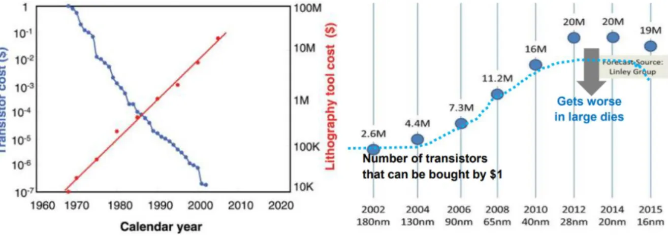
In today’s modern world, nanostructures are becoming a crucial part of almost every device due to the enormous evolution registered in the field over the last 70 years.1 The assembly of nanostructures, structural architectures with at least one nanoscale dimension (~1-100nm), can be obtained by a series of top-down and bottom-up fabrication methods like OL (Optical Lithography) and ALD (Atomic Layer Deposition), respectively.2,3 Figure 1.1 depicts the evolution of lithography and transistor costs throughout the years. Despite being able to produce high-quality micro/nanopatterns, the involved high manufacturing and operation costs, high compound specificity, low large-area substrates compatibility and necessity of complex systems urged the search of new alternatives to fabricate these structures.4–7 Additionally, the number of transistors bought with a fixed price of $1 increases until certain point. From 2014 forward, the number of transistors starts to decrease mainly due to the fabrication processes’ complexity and costs, reinforcing the need for other assembly alternatives.8
Figure 1.1 - Cost evolution of lithography processes throughout the years, related to the transistor costs also.8,9
Techniques based on SL (Soft Lithography), like μCP (micro-Contact Printing)5,7 or RM (Replica Molding)10,11, or NIL (NanoImprint Lithography)12,13 are suitable competitors capable of producing nanostructures and also surpassing most of the mentioned challenges.
1.2 Objectives
This thesis objective resides on the study of nanostructures’ transfer methods that are cheap, simple, scalable to large areas and compatible with a wide variety of substrates and compounds. Therefore, NCA (NanoCombing Assembly) and Rubbing methods were addressed aiming to transfer ordered and random NW (Nanowire) arrays, respectively. To fully assess NCA’s
capabilities, several parameters were studied as PR (Photoresist) layer thickness and morphology, transfer’s speed and pressure and substrates’ surface treatments. Seed layer
synthesized ZnO (Zinc Oxide) NWs were used, being transferred to PR-patterned glass substrates. On the other hand, Solution-based synthesized Ni (Nickel) and ZTO (Zinc Tin Oxide) NWs were delivered, using flat and patterned PDMS (Polydimethylsiloxane), to PR-patterned
glass, flat glass and flat PEN substrates, through Rubbing. Substrates’ surface treatments, NW
Transfer methods for arrays of nanostructures
Transfer methods for arrays of nanostructures
3
2. INTRODUCTION
As the demand for smaller devices keeps increasing, fabrication techniques with higher resolution and aspect-ratio are needed to sustain such miniaturization. Due to the investment put on these processes, production of nanometric components milestone was achieved around the 2000s, as seen in Annex A, which have at least one nanoscale dimension (~1-100nm).14,15 Widely recognized Top-Down methods such as OL (Optical Lithography) and EBL (Electron-Beam Lithography), are the most used by the semiconductor industry5–7 aiming to produce these nanoscale components. However, as fabricated feature sizes tend to continuously decrease, the more complex Top-Down systems become. Inevitably, OL and EBL apparatus are becoming too expensive, as pictured in Figure 1, and other approaches need to be considered.16–18 For instance, a EUV (Extreme Ultraviolet) OL system can cost ≈$50M whether a DUV (Deep Ultraviolet) OL is worth ≈$20M, neglecting its CoO (Cost of Operation) and maintenance, which can be quite expensive too.10 Additionally, these techniques are not compatible with a broad variety of compounds and are not suitable for applications in large-area and thermal-sensitive substrates, thus making them unattractive for the semiconductor industry.
2.1 Bottom-Up Assembly: NWs
Thereby, Bottom-Up approaches were considered as they use nanoscale building blocks to assemble functional nanostructures, instead of standard Top-Down methodologies. NWs (Nanowires) are one-dimensional nanostructures that have been thoroughly studied due to their potential applications in electronic and photonic devices like FETs (Field-Effect Transistors)19–21 and PDs (Photodiodes)22–24, respectively. These structures are commonly composed of metallic and semiconductor materials and can be synthesized by various processes such as CVD (Chemical Vapor Deposition), Solution-Based and Metal Catalyst-Free Growth. NW growth by CVD has several variations like the VLS (Vapor-Liquid-Solid)20,21,25–27 and VSS (Vapor-Solid-Solid)22,28,29 mechanisms but, overall, these are methods that consist on the growth of NWs, mostly semiconductor NWs, using metal clusters/NPs (Nanoparticles) as catalysts. Metallic catalysts are deposited on top of a substrate, a generic semiconductor wafer for instance, and are heated inside a vacuum chamber. Annealing stages proceed, whose temperatures vary according to the type of CVD growth where the eutectic point of the substrate’s material/catalyst
group plays a major part in distinguishing all of its types20,28,29, i.e. the temperature which Au/Si group melts if NW growth is desired on an Au-coated Si substrate, for example. When NW growth is conducted by a VLS process, applied heating must be above the eutectic point, whether by
VSS’s annealing temperatures should be below this point. Afterwards, a gas precursor containing the desired NW compound is introduced inside the chamber where its atoms will attach preferentially to the liquid metal catalyst. Through continuous insertion of the precursor, anisotropic growth will begin, attaining NWs in the end. Annexes B and C present VLS procedure and commonly synthesized NW compounds by VLS, respectively. Solution synthesis30–33 is mostly used when metallic NWs are to be assembled and their production is based on chemical reactions with or without templates. The use of templates22,34,35 such as porous AAO (Anodic Aluminum Oxide) usually helps in the wire’s shaping but are not obligatory. This kind of synthesis
usually requires some catalyst that will promote wire assembly in a solution containing the desired NW compound. Catalysts can be either suspended particles in the solutions or deposited on the growth substrate, acting as a seed layer32,36. Other NW synthesis methods are also reported that do not need metal catalysts such as MBE (Molecular Beam Epitaxy)22,37 or VPE (Vapor-Phase Epitaxy)38,39. Generally, a gas containing the desired NW compounds is inserted in low- or even ultra-low-vacuum atmospheres and their atoms attach to the catalyst on the desired growth surface.
Nevertheless, these processes have some drawbacks regarding the annealing stages, synthesis duration, low-vacuum atmospheres and growth substrates’ compatibility. Despite the high control
witnessed in terms of grown NW’s diameter, length and positioning, CVD and Epitaxy are pricey
Transfer methods for arrays of nanostructures
4
alignment or positioning. By that, if one can focus entirely on attaining the best NW synthesis possible, better approaches can be inspected towards obtaining the best NW arrangement, where Transfer methods can play a major role.
2.2 Transfer Methods: NWs
Along these lines, Transfer methods aim attention at the deposition of pre-grown nanostructures on desired substrates with high uniformity, feasibility and simplicity. Additionally, these methods ought to be cheap, compatible with large-area and/or thermal-sensitive substrates and with a wide variety of compounds. Intending to deliver NWs to a specific substrate, several transfer techniques were reported, in which DRP (Differential Roll Printing)40, SP (Sweeping Print)41, BBF (Blown-Bubble Film)42, WW (Water Wedging)43, NCA (NanoCombing Assembly)44 and Rubbing45 stood out from the rest, since most of the mentioned requirements were attained by each. These methods will be briefly described and their results shown in terms of transferred NWs alignment, NWD and other relevant features. Emphasis is done to the most promising ones, NCA and Rubbing.
DRP40 is a process in which NWs are grown on a cylindric roller and are transferred to the desired substrate upon contact with it. This process is not specific to a certain NW compound or substrate material. The utilized NWs, of semiconductor compounds, are grown by VLS without any sort of positioning, aiming to transfer the highest NWD in the end. Accordingly, NW assembly regions are defined on the transfer substrate with a PR (Photoresist) layer through typical OL and are subsequently functionalized with a 0.1% w/v solution of poly-L-lysine. For transfer speeds under 20 mm/min and using a lubricant, Octane, to minimize contact friction, NWs detach from the roller by cause of VdW (Van der Walls) forces and are delivered to the assembly regions. >90% of transferred wires present alignment with ±5º deviation considering the printing direction, despite being randomly positioned on the assembly regions. PR layer can be removed afterwards with standard lift-off procedures leaving the aligned wires behind. This method can be performed at RT (Room Temperature) on small- and large-area rigid or flexible substrates and a transferred NWD of ≈6 NWs/μm was reported. However, standard lithography like OL is needed to predefine assembly regions and NWs need to be grown on cylindrical rollers every time the process is repeated. Annex D shows the used setup and some transfer results.
SP41 methodology also relies on mechanical forces to transfer NWs to a certain substrate. NWs are grown by CVD on a rigid substrate and are mounted on a fixed stage, with the wires facing downwards, while the transfer substrate is mounted on a movable curved stage facing upwards, with a PDMS cushion between them. ZnO NWs and Kapton substrate were used in the reported trial. The movable plane is connected to an axis that enables circular movement, as shown in Annex E. Upon contact with the ZnO NWs, the Kapton substrate is moved counterclockwise and the wires are transferred due to the applied shear forces. This procedure is done at RT. Transfer results showed a NWD of ≈1.1 × 10⁶ NW/cm2 and a good degree of alignment, as seen in Annex E. However, NW alignment was not measured and they were randomly spread across the Kapton surface with inconsistent lengths.
BBF42 transfer method is based on the contact and popping of a blown polymer bubble, with suspended NWs or NTs (Nanotubes), on a target substrate. Liquid polymer was produced by a mixture of THF and an epoxy resin, where the desired viscosity was attained after 20-30 hours by cause of the curing process. NWs and NTs are added in the THF before mixing the resin. The liquid polymer is then put inside a circular die and N2 gas is blown through it, forming a bubble of liquid polymer with NWs/NTs suspended, as showed in Annex F. Due to the uniform bubble expansion, with the aid of a ring, along a defined direction, a certain degree of NW/NT alignment is attained. Contact of the polymer bubble with the transfer substrate will make it burst, transferring the NWs/NTs to the substrate’s surface without jeopardizing their alignment. This technique was
Transfer methods for arrays of nanostructures
5
transfer to the substrate, and the absence of some NWs/NTs from the bubble’s outer surface,
jeopardizing the yield of the transfer. Additionally, transferred nanostructures were randomly positioned despite the manifested alignment.
WW43 is a transfer process based on the hydrophobic effect and has no mechanical steps like the
ones witnessed in DRP and SP or long preparation times of NW’s suspensions as in BBF. A wide variety of substrates, rigid or flexible, is compatible with the process and nanostructure’s precise
positioning is attained through the use a xyz-probe. To carry out the transfer, a hydrophilic glass slide containing a nanostructure on top of one of its sides is dip-coated with a hydrophobic polymer coating, whose constituent has great affinity with the nanostructure’s material, thus housing it. As it is slowly dipped into water with a defined angle of incidence (30º or 150º considering the water meniscus), this hydrophobic coating will start to peel-off, bringing the nanostructure with it because of the high affinity between one another. When fully submerged, the hydrophobic coating containing the nanostructure will be suspended on the water. The desired substrate is put under water and, using the xyz-probe, transfer can be made by progressively removing the water. To finalize the process, dissolution of the hydrophobic coating is done,
leaving the desired nanostructure on the target substrate. This method’s steps and demonstration are depicted on Annexes H and I, respectively. Transfer can be attained at RT with high positioning precision on large-area substrates. However, water can be trapped between the nanostructure and target substrate when lowering its level, especially if a flexible substrate is used. The polymer coating also needs to be flexible enough to properly detach from the hydrophilic substrate upon dipping. This process was successfully tested by transferring graphene films onto semiconductor wafers and gold patterned films were also delivered but, this
time, with a few problems regarding the hydrophobic coating’s affinity with gold. More importantly and related to this thesis, NW transfer was not reported.
Most of the described transfer methods presented a great compatibility with rigid/flexible substrates, a wide range of NW compounds and were scalable to large-area surfaces but not all
of them present good transfer uniformity and reproducibility. On the other hand, NCA’s outcomes
show a better NW alignment compared to the described methods and Rubbing enables the simplest and most cost-effective transfer of all, despite not guaranteeing any sort of nanostructure alignment in the end. Detailed description of these two processes is done below.
2.2.1 NanoCombing Assembly, NCA
44NCA is similar to DRP since a flat NW growth surface is used instead of a cylindrical roller to perform the transfer onto a PR-patterned substrate by friction. It aims to transfer highly ordered NW arrays with precise positioning. Reported results were obtained by transferring seed
layer-grown Si NWs, with an average length of 30 μm, onto a PR-patterned substrate through direct
contact between one another. Upon contact between both substrates, NWs’ anchoring will occur
on the exposed substrate areas. With constant pressure and speed, subsequent dragging of the seed layer substrate with determined direction will rip off NWs from the seed layer, transferring them. The final seed layer substrate movement originates friction that will induce the NW alignment, thus obtaining ordered arrays on top of the PR layer. Figure 2.1 depicts the process in its integrity.
Transfer methods for arrays of nanostructures
6
Yao et al.44 stated that the need to have two very distinct, separate regions in the transfer substrate is imperative so anchoring and combing (or alignment) regions, AR and CR
respectively, were carefully designed and optimized through OL. AR is a defined substrate’s area
that needs to have a strong interaction with the NWs so it’s surface roughness and hydrophilicity
need to be maximized. On the other hand, CR has to be exactly the opposite: a hydrophobic and planar surface, to minimize the interplay with the NWs. This difference will magnify the alignment
forces since the NWs will be strongly anchored in AR and weakly adhered to CR’s surface, making it very susceptible to the transfer’s movement direction. AR is illustrated in Figure 2 as the exposed substrate areas in blue and CR as the PR-patterned layer in green.
Some important studies were conducted in this report, regarding AR/CR critical dimensions and NWD optimization. First, AR length needs to be at least 15 μm to maximize NWD, registered at 1,5 NW/μm. In this point, NWD saturates and stays put beyond it (Annex J and K(a)). This region is critical since it is here that the NWs will anchor one of their two edges, thus needing an adequate area to trap the highest number possible. If the AR is, by chance, smaller than 15 μm, so will be the transferred NWD. Secondly, CR layer cannot be thicker than 70 nm as NWD will decrease for greater sizes, caused by the lower probability of NW/AR contact. Annex K presents these relations. Additionally, transfer applied force and speed during the process were studied, showing a large independence of NWD whenever they stand between 2-6 N/cm2 and 2-20 mm/min, respectively. Forcing the substrates too much against one another will likely damage the structures as well lower the NWD. Likewise, moving them too fast lessens the contact odds. Annex L exhibits these relations.
NCA transferred wires showed a higher degree of alignment compared to the previously stated, exhibiting 98.5% aligned NWs with ± 1º misalignment, thus showing very few crossing defects in the transferred arrays. Likewise, transfer speeds between 2-20 mm/min did not alter the final alignment, as shown in Annex L(a). More testing was done to assess the process’ scalability and
flexibility. Good alignment ratios were attained when transferring NWs to a 3x11 mm2 area patterned with alternating 15x80 μm2 sections. (Annex M) Also, bigger transferred wires were obtained when pre-grown NW were bigger but a large part of them is lost during the process. For instance, 30-μm long synthesized SiNWs end up 7-μm long in the end, owing to Friction (≈50%) and excessive trapped NW length in the AR (≈25%). Moreover, ≈140 μm-long NWs were successfully transferred with a 96% alignment within a variation of ± 1º. (Annex N) All of these experiments show the remarkable attributes that NCA has and shows the process’ compatibility
with bigger substrates and ability to transfer highly ordered NW arrays.
2.2.2 Rubbing
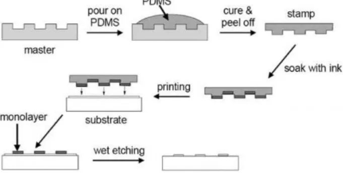
45Despite the mentioned output of NCA, it still relies on costly lithography to prepare substrates for transfer, for example. The Rubbing technique has a very similar procedure to a common SL method, as depicted in Figure 2.2, and the low-cost, simplicity and operation at RT are its most relevant attributes.
Figure 2.2 - Common SL methodology from the replica production until the end-product. This scheme is inspired in a reported SL process.46
Transfer methods for arrays of nanostructures
7
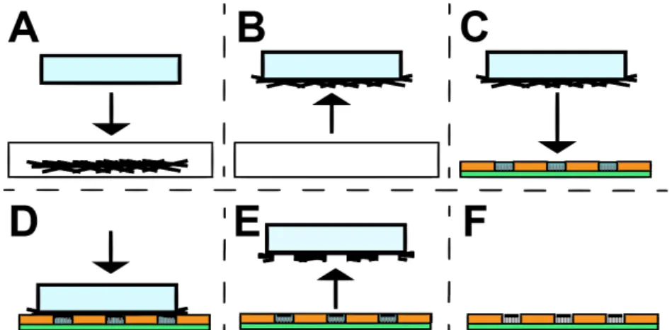
Initially, a GZO (Gallium-Zinc Oxide) coated glass substrate is patterned with a PR layer and ZnO NRs are grown vertically in the exposed GZO zones. To perform the transfer, a flat PDMS slab is rubbed with circular motion (Annex B, (a)) on top of a uniform CuO NR layer. As it is only desired
to have the transferred NRs on top of ZnO rods, water is placed in the PR’s cavities, precisely
where ZnO NRs are. Pressing the PDMS attached-CuO layer on the patterned surface and freezing the water afterwards, will trap the rods on those specific zones. Subsequent PDMS peeling leaves the CuO NRs only on the desired locations and a final heating step is done to evaporate the water. In the end, a random compact CuO NR layer is deposited on top of ZnO NRs. Despite the initial lithography step, Rubbing is a technique independent of it since this beginning stage was only used to transfer in the desired areas. The whole process is depicted on Figure 2.3.
Figure 2.3 - Rubbing transfer method reported by Biswas et al.45. (A) represents the PDMS
(light blue) rubbing step on CuO NRs and posterior removal, (B). Water droplets are delivered on the exposed substrate areas, (C), aiming to cover the exposed ZnO NRs (gray vertical lines) completely when the PDMS is pressed. (D) shows the contact step between both CuO NRs-coated PDMS and the patterned substrate. After freezing, the PDMS is peeled off, (E), leaving the CuO NRs (black horizontal lines) on top of the ZnO NRs (F). Glass substrate and PR patterns are illustrated in green and orange, respectively.
2.3 NW Compounds
Transfer methods for arrays of nanostructures
Transfer methods for arrays of nanostructures
9
3. MATERIALS & METHODS
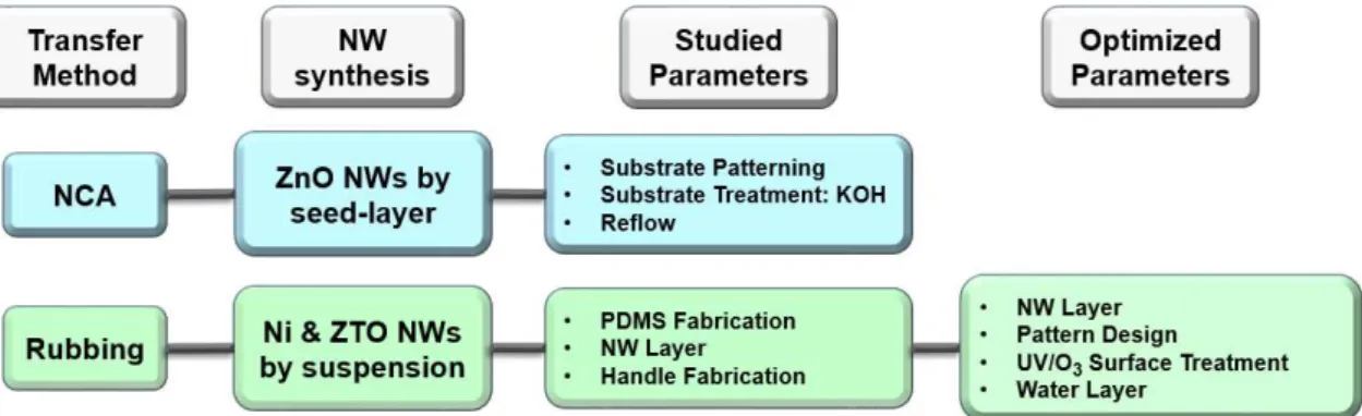
In order to successfully reproduce the previously described techniques, NCA and Rubbing, all of its elements need to be carefully studied and optimized. The following scheme in Figure 3.1 presents a summarized view of this work and all the addressed features for each method, from left to right.
Figure 3.1 - Scheme for this work’s addressed elements for each technique, from left to
right.
3.1 NW synthesis
3.1.1 ZnO NWs by Seed Layer-Assisted Solution Method
54Initially, ZnO seed layer (~5 nm thick) was deposited on piranha cleaned glass substrates via sputtering. For the growth of nanowires, synthesis was carried out in a 100 mL autoclavable bottle containing aqueous solution mixture of hydrated zinc nitrate (Zn(NO3)2·6H2O) and hexamine (HMT, C6H12N4). The seeded substrate, which was mounted on a glass slide, was kept within the solution, keeping the seeded face downward. The bottle was kept in an oven at 95̊ C for 6h. Afterwards, bottles were allowed to cool down to room temperature naturally and the substrates coated with white layer were washed thoroughly with DI water. Finally, the substrates were dried at room temperature. This synthesis was carried out by Dr. Soumen Maiti from CENIMAT.
3.1.2 Ni NWs
55and ZTO NWs
56by Solution Method
Ni NWs synthesis process is based on a solution method in which Ethylene Glycol is mixed with Nickel(II) Chloride (NiCl2·6H2O) in a glass beaker. The solution is put for 10 min. under 120ºC heating. Later, Hydrazine Hydrate (N2H4·6H2O) was added to the mix and another heating step was done for 1 hour at 120ºC, finalizing the synthesis.55 This synthesis was carried out by MSc Rodrigo Santos from CENIMAT.
ZTO NWs production is also based on a solution method, where 0.04M of Zinc Chloride (ZnCl2), 0.02M of Tin(IV) Chloride (SnCl4·5H2O), 0.24M of Sodium Hydroxide (NaOH), 7.5 mL of H2O and 7.5mL of Ethylenediamine are mixed in an autoclave reactor. Posteriorly, the reactor is put in an oven at 200ºC for 24 hours, attaining the ZTO NWs. The resulting wires are washed several times with copious amount of H2O and IPA, alternately. Finally, ZTO NWs are dried in a vacuum bell jar for 2 hours at 60ºC.56 This synthesis was carried out by PhD Student Ana Rovisco from CENIMAT/CEMOP.
3.2 NanoCombing Assembly: Transfer of ZnO NWs
Transfer methods for arrays of nanostructures
10
3.2.1 Substrate Preparation
PR thickness of 70 nm is needed to establish the distinct anchoring and combing regions44. AZ® ECI 3012 was chosen and is a positive resist recommended for DUV Lithography processes. Spin-coated films are 1.2 μm-thick at 4000 rpm but can vary from 1.0 to 2.2 μm with different spin-coating parameters. To obtain the desired thickness, dilution needed to be done and ≥99.5% PGMEA (Propylene Glycol Monomethyl Ether Acetate, Sigma-Aldrich®) was the adequate thinner. Different PR:Thinner volumetric ratios were used, from 1:3 to 1:5, to fully assess the resulting thicknesses. Dilution ratios were recommended by MicroChemicals® staff.
To deposit the PR, common 10x10 cm2 glass substrates were cut into 3x3 cm2 pieces. These were cleaned in ultrasonic baths in successive steps: 10 min. Acetone followed by 10 min IPA. Glass substrates were then rinsed with DI Water to remove IPA excess and dried with N2 Drying Pistol. Then, substrates were put on a heating plate at 115ºC for a few seconds to ensure no water is on their surfaces.
Afterwards, film spin-coating was done with SUSS Microtech Spinner using a two-speed sequential deposition: 10-sec at 3000 rpm and 20-sec at 4000 rpm. Diluted PR volume applied for spin-coating was 1 mL. After this, a soft bake was done for 1:15 mins at 115ºC.
Sample exposure follows to pattern the PR layer. The mask used for this stage was an I3N mask with 700 μm-wide and 2.5 cm-long tracks with 700 μm-wide gaps between them. On one of their edges, microelectrode contacts were patterned. Exposure was done with a KARL SUSS UV MA6 aligner for 3.5 sec in Soft-Contact mode, in which the mask is gently pressed against the PR-coated glass substrate. PEB (Post-Exposure Bake) at 110ºC for 1 min. follows to ensure proper PR patterning.
PR Development was performed with consecutive Merck® AZ MIF 726 developer 30-sec bath and two DI Water 30-sec baths.
Finally, HB (Hard Bake) was done with different temperatures for 1 min, as it will be explained in the Results section, thus finishing the lithography process.
3.2.2 Transfer Setup
To reproduce identical NCA transfer, a setup was experimented using a Film Applicator BYK Gardner to move the seed layer substrate on top of PR-coated glass substrate at constant speed. Since constant pressure needed to be done, a weight was put on the back of the seed layer substrate so it would apply the pressure evenly. Two identical glass slides were attached to the glass substrate with PR surface faced upwards, creating a long path to perform the technique. Just before transfer trials were executed, 40 μL of Baysilone M-350 Lubricant were added next to the PR-coated glass, the same volume used in the report.
When using the film applicator, the fixed weight on the seed layer substrates back enabled the
movement. The system’s beam was programmed to move at minimum speed (50 mm/sec) and, upon touching the weight, it would slide the ZnO NW seed layer on the PR-coated glass substrate, just after passing by the Baysilone liquid volume. Figure 3.2 shows the devised setup:
Figure 3.2 - NCA inspired transfer setup in which are pictured the patterned glass substrate (1), glass slide (right and left of the patterned substrate) (2), Baysilone Lubricant (3), Weight (4) and Film Applicator Beam (5). Note that the ZnO NWs substrate location is only representative since it was not positioned above the Weight, having the wires (black dots)
Transfer methods for arrays of nanostructures
11
3.2.3 Substrate Treatment: KOH solution
Initially, glass substrates were immerged in a 1.5% wt. KOH (Potassium Hydroxide) solution to improve their hydrophilicity and later in less concentrated solutions to prevent harmful reactions with the PR tracks, as it will be explained in the Results section. To develop a 100mL 1.5% wt. solution, ≈1.7 grams of ≥90% pure KOH flakes (Sigma-Aldrich) were mixed with ≈98.3 mL of DI Water by stirring. Other solutions used throughout this work were 0.5% wt. and 0.25% wt. solutions. For the 100 mL 0,5% wt. solution, ≈0.5 grams of the same KOH reagent were mixed with ≈99.5 mL of DI Water and, similarly, ≈0.25 grams of KOH flakes were mixed in ≈99.75 mL to produce the 0.25% wt. solution. All 3 solutions were conserved in separate covered glass flasks.
3.2.4 Reflow Trials
Reflow tests were done to alter the PR tracks roughness and square-edged profiles. According to the datasheet, a deliberate hotter HB step would diminish the sharpness of PR profile edges, thus obtaining a rounded PR track, like shown in Figure 3.3:
Figure 3.3 - Reflow tests and its effect on PR’s profiles with increasing temperature. Taken from AZ® ECI 3012 datasheet.57
The main goal behind this experiment was to create softer tracks so that, upon combing, NWs would not break due to the sharp corners, attempting to improve the process’ yield regarding
combed NW length.
Likewise, different Development times were performed to check their influence on PR’s profile.
3.2.5 Characterization
Fabricated Pattern PR tracks on glass were analyzed using Profilometer Sloan DEKTAK3, Profilometer Ambios XP200 and Asylum Research MFP3D Standalone AFM. AFM imaging was taken in Tapping Mode with Olympus AC160TS (K=26 N/m; FØ=300 kHz) and then processed with Gwyddion software.
Transfer results were inspected with Optical Olympus BX51 Microscope and processed through software Cell^A.
Substrate treatment was examined through contact angle measurements using Dataphysics OCA15plus equipment and software by Sessile-drop methodology. Water volume used for the measurements was 1 mL.
3.3 Rubbing Transfer of Ni and ZTO NWs
In order to perform transfer based on the Rubbing method, a uniform layer of NWs has to be attained, whose production is explained below. Solution-based NW synthesis was chosen since the wires are suspended in the end-product solution and can be stored in powdered form when removed from the solution. Also, the wires can be suspended in IPA without affecting their properties. Transfer based on Biswas et al.45 uses PDMS as transfer layer for the NWs. These wires were dried and kept in powdered form to enable this use of PDMS, thoroughly explained below. Flat and Patterned PDMS were used to perform the transfers. Several substrates were tested as templates for the NW deposition: PR-coated Glass, whose fabrication is explained above, flat glass and flat PEN sheet.
3.3.1 PDMS Production
Transfer methods for arrays of nanostructures
12
of the Curing Agent needed to be blend together to attain the ratio. Afterwards, the end-product needs to be mixed very well until it is full of bubbles. With a vacuum bell jar, sample was put under low-vacuum to remove all the bubbles, resulting in clear viscous PDMS. The mix was then poured
in a plastic petri dish and was inserted in an oven for 1 hour at ≈65ºC to perform the curing step. If PDMS pouring creates more bubbles, they must be removed with the vacuum bell jar again, so that a uniform PDMS block is attained. Finally, the soft PDMS block was demolded from the petri dish and ready to be handled.
3.3.2 NW layer
In order to obtain a layer of synthesized NWs by solution-based methods, as explained above, one must disperse them in a liquid medium. For both compounds, Ni and ZTO, a small amount of them was mixed with a certain volume of IPA in a glass cylindrical vial. Through the use of an ultrasonic probe, the NWs were fully dispersed in IPA. This step lasts for at least 5 minutes to avoid NW aggregation. Afterwards, solution was put in petri dish and left to rest overnight to evaporate the IPA. In the end, a uniform layer of NWs was deposited on the petri dish’s bottom,
ready to be transferred.
3.3.3 Transfer Setup: Flat PDMS with Flat & Patterned Glass
PDMS integration caused some changes in the process. No longer using seed layer-grown NWs, small PDMS squares were cut from its production output. These were rubbed on top of the NW layer so that they could be deposited on the desired substrate.
To perform the transfer, DI water was used as a transport medium for the NWs. Some droplets of DI Water were put by hand on a chosen transfer area and the NW-covered PDMS surface was brought into conformal contact with the PR-coated glass/Flat glass where the water drops were positioned. Downward pressure is applied on the PDMS and excessive water amount is removed with filter paper. The whole group is then inserted in a freezer to solidify the water layer for at
least 5 mins. It is extremely important to guarantee a proper water freezing so this step’s time can
be extended. Then, the PDMS layer was detached, leaving the NW on top of the glass substrate since the ice trapped them. Finally, the sample is put on a hot plate at ≈105ºC for a couple of seconds with the sole purpose of evaporating the water, leaving the NWs on the initially desired zone. This step is also very important and needs to be done quickly since the final patterned NW layer can be ruined if the water liquifies again.
3.3.4 Transfer Setup: Patterned PDMS and Flat Glass
Thereafter, transfer process using a patterned PDMS layer instead of patterned glass was executed. In order to pattern the PDMS, acrylic masters were done with a Laser System VLS3.50 Cutting Machine. Working with a 3-mm thick acrylic surface, desired patterns were designed with Adobe™ Illustrator software and carved in the acrylic surface. Patterns were then cut individually with the laser cutting machine.
Also, before PDMS patterning, acrylic masters need to go through silanization to ease PDMS peel-off. This stage was performed using a plastic vacuum chamber and PFOTS (trichloro (1H, 1H, 2H, 2H-perfluorooctyl) silane (97 %), Sigma-Aldrich). Inside the chamber, a plastic petri dish serves as a container for the silane compound, in which 2-3 droplets of it will be inserted. Acrylic
masters are put in the chamber’s dish and vacuum was done for 30 mins using a vacuum pump.
Afterwards, air is admitted inside the chamber and acrylic masters are ready to use.
As mentioned in “PDMS production” section, after bubbles are removed using the vacuum bell jar, PDMS mix is poured in a plastic petri dish. To produce the master’s replicas, pre-cured PDMS needs to be shed on top of the acrylic masters before its final curing stage. Two different paths
were followed to produce the masters’ replicas: Spin-Coating and Pouring. When spin-coating, PDMS is settled on top of the patterned acrylic masters and spinned at a maximum speed of 250 rpm for 1,5 minutes. The sample is taken to the oven at 85ºC for 1,5 minutes (curing time is
significantly lower than the stated at “PDMS Production” section since spin-coated PDMS has a much lower thickness) and subsequently detached from the acrylic master. If a bigger PDMS replica thickness is desired, the acrylic master molds are put inside the petri dish with their pattern facing upwards. Then, PDMS is poured on top of it, almost filling the petri dish, as pictured in Figure 3.4. It is very important to check if the pattern is in contact with the dish’s bottom to obtain
Transfer methods for arrays of nanostructures
13
described in “PDMS Production” section. Ultimately, the soft PDMS block is cut by the boundaries
of acrylic piece and detached from it, obtaining the patterned PDMS replica.
Figure 3.4 - Acrylic PDMS replica fabrication. This sequential process is done from left to right in which are pictured the PDMS layer (1), the Acrylic master (2) and the Petri dish (3). As described, PDMS block is demolded and then cut by the boundaries of the master. Patterned PDMS is posteriorly detached.
Using the Patterned PDMS chunks to transfer does not change the described process in the previous section. So, PDMS was put into contact with the NW layer and later in contact with the desired substrate, flat glass. Water was sandwiched between NW-coated PDMS surface and flat glass surface. Taking the whole system to freeze will trap the NWs inside the ice and upon
detachment, these wires will remain on the glass’ surface. A final step of heating using the same
temperature will evaporate the water, thus finishing the transfer.
3.3.5 Stamp Handle Fabrication
To pressure the PDMS stamp uniformly against the glass substrate, a handle was printed using
a 3D Printer. Patterned PDMS was attached to the holder’s square surface using a double-sided tape, with its pattern facing downwards. Additionally, the handle’s weight will help improve the technique’s water freezing step, maintaining a certain pressure on the PDMS thus keeping a larger amount of NW immerged in the water layer. The handle’s 3D model is pictured on Figure 3.5:
Figure 3.5 - 3D model of the used stamp handle/holder. Square holder has a 4x4 cm2 area whether the handle is ≈5cm tall.
3.3.6 Transfer Setup Optimization: NW & Water Layer and Pattern
Design
Initially, when PDMS was implemented in the transfer process, the NWs mass was not weighted and a big chunk of wires was transferred but to obtain a proper uniform layer, mass needs to be considered so that transfer results can be compared accurately. Hence, a fixed mass of NWs was weighted then mixed with a certain volume of IPA and an ultrasonic probe was used to disperse the wires. The solution was poured into a square plastic box and left to rest overnight to evaporate the IPA, obtaining a more uniform NW layer.
The water layer is also very important for the success of this process. However, dropping a few droplets of water on top of the transfer substrate is an unprecise stage of the process. Water spin-coating was then considered aiming to obtain a uniform layer on top of the transfer substrate. Several tests were done and a recipe was obtained to deposit the water layer: 750 rpm for 5 seconds. The used spin-coater was a Spinner Laurell 2 (WS-650Mz-23NPP).
Additionally, after using KOH solutions to enhance substrates hydrophilicity, another treatment was tested: UV Ozone cleaning. KOH solution immersion achieved very good results within a short time but the KOH film uniformity was not consistent since, when dried, it left some spots on
Transfer methods for arrays of nanostructures
14
3.3.7 Characterization
NW layer uniformity was inspected through the use of Optical Olympus BX51 Microscope and software Cell^A. Transfer results were also analyzed by the Optical Microscope and through SEM Hitachi TM 3030Plus Tabletop and SEM-FIB Zeiss Auriga CrossBeam Workstation.
Transfer methods for arrays of nanostructures
15
4. RESULTS
4.1 NWs Synthesis
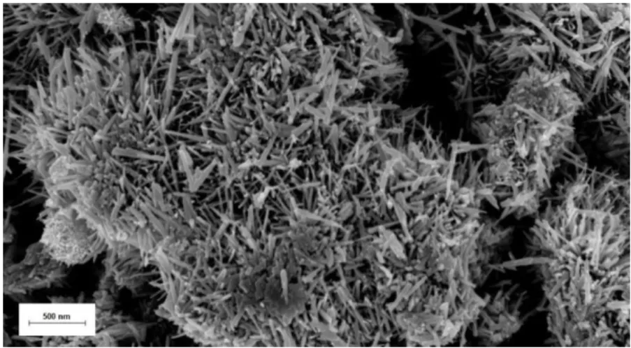
ZnO NWs were grown on a ZnO seed layer using the procedure explained in Materials & Methods Chapter. Measured NW lengths and diameters stood between 1.4-1.8 μm and 110-190 nm, respectively, as shown in Figure 4.1. Wires’ production and evaluation were done by Dr. Soumen Maiti from CENIMAT.
Figure 4.1 – SEM image of grown ZnO NWs by seed layer: lateral (Left) and top view (Right).
Ni NWs were grown by a solution-based procedure, explained in Materials & Methods Chapter. Synthesized wires had lengths of ≈60 μm and diameters of ≈1.9 μm on average, as represented in Figure 4.2. These NWs are formed through the agglomeration of Ni NPs, which are characterized by a rougher surface compared to the other used NWs.58 Ni NWs were produced by MSc. Rodrigo Santos.
Figure 4.2 - SEM image of synthesized Ni NWs by a solution-based method.
ZTO NWs were also synthesized by a solution-based method, addressed in Materials & Methods Chapter. The wires were produced by PhD student Ana Rovisco and had lengths and diameters of 600 nm and 80 nm on average, respectively. Figure 4.3 shows the produced wires.
Transfer methods for arrays of nanostructures
16
4.2 NanoCombing Assembly: Transfer of ZnO NW synthesized by
seed-layer solution method
NCA procedure44 implied the fabrication of patterned glass substrates in which AR and CR need to be well-defined so that similar NW transfer can be performed. PR coating and patterning on glass, identical to the assembled by Yao et al.44, was done using a OL system. To do so and as explained in the Methods chapter, PR needed to be mixed with an adequate thinner using different volumetric ratios. PR dilution is crucial to the process since a proper PRT (PR Thickness) is required.
4.2.1 Substrate Fabrication: Photoresist Dilution
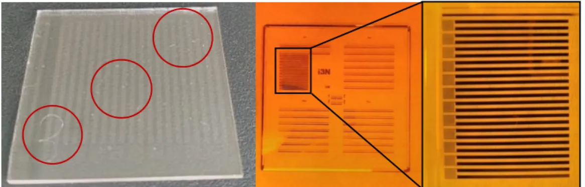
To obtain the necessary thickness of PR film on the glass, dilution tests were done using PGMEA as its thinner. Initially, 3 different PR dilution ratios were examined (PR:Thinner). PR layers were deposited on top of 3x3 cm2 flat glass substrates but were not submitted to PEB and HB steps since in the end of the transfer process, after the NWs are combed, PR layer needs to be removed. PEB and HB stages aim to improve the desired pattern’s resolution and toughness, respectively, but, as stated, PR removal finishes the process and it may prove to be very hard if these baking steps are done.59 Figure 4.4 depict the final outcome of the OL procedure and used exposure mask.
Figure 4.4 - 3x3 cm2 PR-coated glass substrate (Left). The microelectrodes pattern area
can be seen near the sample’s ID number, 3. Red circles represent measurement
locations, as explained below. Also, patterned Mask and section used in OL are pictured in the Center and Right, respectively.
PR thickness of these samples was evaluated through the use of Profilometer Sloan DEKTAK3, whose results are presented in Table 4.1. Height assessment was done in three different sample
areas: Center, close to the sample’s ID number and on the opposite of the ID number. In each spot, three measurements were done.
Table 4.1 - PR tracks heights of tested 1:3, 1:4 and 1:5 dilutions.
Dilutions 1:3 and 1:4 ought to be the most promising towards obtaining 70 nm thickness. Like so, dilution ratios were tested and analyzed again using Profilometer Ambios XP200. This time however, the used dilutions were 1:3, 1:3.5 and 1:4, and were measured in five different sample
Dilutions (PR:Thinner) Measurement Position Thickness (nm)
1:3
Centered 77,8
Close to ID 83,5
Opposite to ID 84,5
1:4
Centered 47,4
Close to ID 41,5
Opposite to ID 48,4
1:5
Centered 35,9
Close to ID 30,5
Transfer methods for arrays of nanostructures
17
spots, three times: Centered, TLC (Top Left Corner), TRC (Top Right Corner), BLC (Bottom Left Corner) and BRC (Bottom Right Corner). Results are shown in Table 4.2.
Table 4.2 - PR tracks heights when 1:3, 1:3.5 and 1:4 dilutions were tested.
When comparing both tests, different thicknesses were obtained using the same dilutions, which is probably due to the age of the used PR, which was replaced later as mentioned in section 4.2.4. Nevertheless, the 1:4 dilution presents the best results of all dilutions. The 1:3.5 dilution also showed good results but with bigger PR height fluctuations, as we can see in Figure 4.5 when comparing 2 measurements taken from the exact same area.
Figure 4.5 – Profilometer measurements and comparison of PR track profiles in the same area with different dilutions. Plot data was leveled.
In conclusion, the used PR, AZ® ECI 3012 is an adequate PR for the process and 1:4 dilution was the chosen one for the transfer process by cause of a more uniform thickness throughout the glass samples.
4.2.2 Transfer Setup
After the PR dilution, a similar NCA setup was designed to test the transfer methodology and infer the best improvements for it. The assembled system relies on the use of a film applicator and a weight, as explained in the Methods chapter. However, PR-coated substrate is not functionalized
and the NWs’ length is way smaller compared to the Si NWs used by Yao et al.44, ≈30 μm (vs 1,4-1,8 μm). Figure 4.6 shows the whole assembly.
Dilutions
(PR:Thinner) Measurement Position
Thickness (nm)
1:3
Centered 107 ± 2
TLC 105 ± 1
TRC 106 ± 1
BRC 103 ± 2
BLC 104 ± 2
1:3,5
Centered 65 ± 5
TLC 67 ± 8
TRC 66 ± 7
BRC 67 ± 7
BLC 72 ± 6
1:4
Centered 67 ± 1
TLC 69 ± 2
TRC 64 ± 2
BRC 66 ± 3
Transfer methods for arrays of nanostructures
18
Figure 4.6 - Weight (Left), which was used to stick the seed layer substrate, and the setup (Right) to perform the transfer Note that, according to the sketch shown in Methods chapter, the weight is positioned on the glass tracks with the seed layer surface facing downwards, i.e. NWs are in contact with the glass track..
Promoting constant pressure, the weight was used to simulate the applied pressure reported by Yao et al.44. It is mentioned that, to avoid decreasing final NWD, a 2 to 6 N/cm2 pressure is enough to promote reliable NW contact with the ARs. In order to do it, a weight was added to the system, as pictured in Figure 4.6. Several items were weighted and the one pictured above was the best among the rest, as proved below in Equation 4.1. This piece weighs ≈1.34 kg and the seed layer substrate has an area of 1,5x2 cm2.
𝑃 =
𝐹𝐴⇔ 𝑃 =
1,34 𝑘𝑔3 𝑐𝑚2⇔ 𝑃 =
1,34 𝑘𝑔∗0,1𝑘𝑔1𝑁
3 𝑐𝑚2
⇔ 𝑃 =
13,4 𝑁
3 𝑐𝑚2
⇔ 𝑃 = 4,47
𝑁
𝑐𝑚2
= 4,47 × 10
4𝑃𝑎
(Equation 4.1)Hence, this weight is acceptable to apply the needed pressure between 2 to 6 N/cm2. Likewise, its shape was perfect for the process since it is similar to a square prism and did not touch
anything else besides the seed layer substrate’s back, when settled on the glass slides.
Evenly important, transfer speed was also checked but it was very different from reported. Yao et al.44 stated that, to maximize NWD, transfer velocity should be within the range of 2-20 mm/minute and, in NCA, a 5 mm/minute speed was used. The film applicator moves its beam at a minimum speed of 50 mm/second, or 3000 mm/minute, an unquestionably enormous contrast. Unfortunately, this proved to be very challenging. Additionally, the lack of surface functionalization and long seed-layer grown NWs made further testing unreasonable.
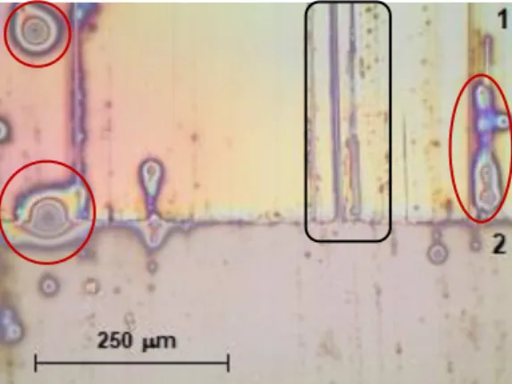
Transfer results can be seen in Figure 4.7, in which the same lubricant volume reported was used, 40 μL. These proved to be a failure since no wires were transferred and the PR tracks were scratched and sometimes ripped off the glass substrate. The main reasons behind these results could revolve around the used weight, the transfer speed and the used NWs length.
Transfer methods for arrays of nanostructures
19
4.2.3 Substrate Treatment: KOH solution
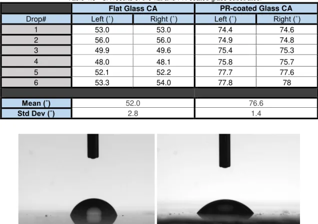
After the unsatisfactory results of the assembled system, glass surface treatment was considered to promote a better NW adhesion to the ARs. Initially, CA (Contact Angle) analysis was done to flat glass and PR-coated glass substrates using the Dataphysics OCA15plus equipment (Annex O). The PR-coated glass surface was not patterned to ensure a proper assessment so one half of the sample is coated with PR and the other is not. Table 4.3 and Figure 4.8 exhibit the CA results for Flat and PR-coated Glass.
Table 4.3 - CA results of the flat and PR-coated glass substrates.
Figure 4.8 – CA measurements of 1 mL water drop on top of the PR-coated (Left) and Flat Glass (Right) surfaces.
Since it is of best interest to have a highly hydrophilic glass surface (AR) and a highly hydrophobic PR coating (CR), suggested KOH treatment by Yao et al.44 was considered: a 50 second bath in a 1,5% wt. KOH solution. Hence, two experiments were done to evaluate the influence of the KOH treatment on glass and PR.
First off, a 3x3 cm2 glass was coated with PR in one half whether on the other half was done nothing, as done above. PR coating was produced according to section “Substrate Fabrication: PR Dilution”. The sample was then immersed in 1,5% wt. KOH solution for 50 seconds and
analyzed through CA measurements. Figure 4.9 shows the outcome of this test.
Figure 4.9 - CA evaluation of both surfaces when submitted to the KOH solution in the end. Flat Glass is on the left whether the PR surface on the right.
Flat Glass CA PR-coated Glass CA
Drop# Left (˚) Right (˚) Left (˚) Right (˚)
1 53.0 53.0 74.4 74.6
2 56.0 56.0 74.9 74.8
3 49.9 49.6 75.4 75.3
4 48.0 48.1 75.8 75.7
5 52.1 52.2 77.7 77.6
6 53.3 54.0 77.8 78
Mean (˚) 52.0 76.6