Engineering of Metal Oxide Nanoparticles
for Application in Electrochemical Devices
Dissertação para obtenção do Grau de Doutor em
Nanotecnologias e Nanociências
Orientador:
Doutora Elvira Maria Correia Fortunato,
Professora Catedrática, Faculdade de
Ciências e Tecnologias da Universidade
Nova de Lisboa
Co-orientador: Doutor Luís Miguel Nunes Pereira,
Professor Auxiliar, Faculdade de Ciências
e Tecnologias da Universidade Nova de
Lisboa
Júri:
Presidente: Professor Doutor Fernando José Pires Santana Arguentes: Prof. Doutora Verónica Cortés de Zea Bermudez
Prof. Doutora Maria Goreti Ferreira Sales
Vogais: Professor Doutor Rodrigo Ferrão de Paiva Martins Prof. Doutora Florinda Mendes da Costa
Prof. Doutora Maria Manuela Silva Pires Silva Prof. Doutor Pedro Miguel Cândido Barquinha
i
Engineering of Metal Oxide Nanoparticles for
Application in Electrochemical Devices
Dissertação para obtenção do Grau de Doutor em
Nanotecnologias e Nanociências
Orientador:
Doutora Elvira Maria Correia Fortunato,
Professora Catedrática, Faculdade de
Ciências e Tecnologias da Universidade
Nova de Lisboa
Co-orientador: Doutor Luís Miguel Nunes Pereira, Professor
Auxiliar, Faculdade de Ciências e
Tecnologias da Universidade Nova de Lisboa
Júri:
Presidente: Professor Doutor Fernando José Pires Santana Arguentes: Prof. Doutora Verónica Cortés de Zea Bermudez
Prof. Doutora Maria Goreti Ferreira Sales
Vogais: Professor Doutor Rodrigo Ferrão de Paiva Martins Prof. Doutora Florinda Mendes da Costa
Prof. Doutora Maria Manuela Silva Pires Silva Prof. Doutor Pedro Miguel Cândido Barquinha
iii
Engineering of Metal Oxide Nanoparticles for Application in
Electrochemical Devices
Copyright © Lídia Sofia Leitão Santos, Faculdade de Ciências e Tecnologia,
Uni-versidade Nova de Lisboa.
v
Acknowlegments
Even if my PhD took four years to complete, I will take this opportunity to appreciate all the people that, by one way or another, helped me to get here and finish this work.
First I would like to thank my supervisors, Professor Elvira Fortunato and Professor Luis Pereira for helping me planning this work, giving new ideas and discussing the results. Thank you for all your support and enthusiasm throughout this years. You are both responsible for me getting here!
To Professor Rodrigo Martins, together with Professor Elvira Fortunato, for being an ex-ample in achieving and retrieving, always, for better results, as well as, giving me all the tools to get there and, allowing to develop this work in DCM and CENIMAT facilities.
To Fundação para a Ciência e Tecnologia for the fellowship (SFRH/BD/73810/2010) that assured me these four years of work experience.
To the actual and former colleagues in CENIMAT and DCM that share the work, lab, lunch and breaks with me: Pedro Barquinha, for your expertise and fruitful discussions; Sonia Pereira e Alexandra Gonçalves, for helping in all what it is needed in the lab; Ana Ramos e Sofia Cruz, main accompaniers in the beginning of this work; Pawel Wojcik, Joana Pinto, Joana Neto, Daniela Gomes, Tomás Calmeiro, for our enthusiastic debates around science in general; Daniela Sal-gueiro, Diana Gaspar and Ana Baptista, also for sharing the room with me; Andreia Cardoso, Mafalda Costa, Antonio Vincente, Tiago Mateus, Ricardo Ferreira, Ana Catarina, Raquel Barros, Paulo Duarte, Jonas Deuermeier, Asal Kiazadeh, Ana Rovisco, Jorge Martins, Cristina Fer-nandes and the rest of the group, I really enjoy working, and sharing the daily life with all of you!
To Paulo Manteigas, Susana Mendes, Patricia Carrão, Valeria Gomes, Carla Saldanha, Sara Oliveira and Sónia Seixas for all the help and support in all the bureaucratic issues.
To Professor Gabriela Almeida and Dr. Célia Silveira for all your help and patience in in-troducing me in the field of electrochemistry and biosensors, as well as, sharing the lab facilities in REQUIMTE, FCT/UNL.
To Dr. Smilja Todorovic for your support with the Raman measurements in ITQB and with the writing of the article.
To Prof. Jaime Viegas and Dr. Elamurugu Elangovan for your time and help doing the TEM images in i-Micro, Masdar Institute of Science and Technology.
To all my friends that I got on the way, Alberto Batista and Diana Marcelino, Rafael Vidigal and Andreia Silva, Diogo Duarte and Filipa Alcaide, Carla and Ricardo Pinheiro, it was a real pleasure to meet you!
vi
A special thanks to Rita Branquinho since you are, in fact, the person responsible for me being here in CENIMAT, so thank you for that and for putting up with me for all these years!
To all my very “old” friends from Peniche (the real “amigos de Peniche”), Hélia Janardo, Ricardo Rodrigues, Carla Franco, Agnelo Rodrigues, Teresa Marreiros, David Vieira, Nuno Franco, Elina Costa, Ana Ferreira, Lena Simões, Hélder Blayer and Ivone Ribeiro (you are also a little bit from Peniche!) for sharing so many good times with me, I appreciate all of it!
To my family… No words to explain how important you are to me! To my mom, you are the main responsible for me being who I am, thank you for everything, my brothers, Paulo e Cajó, you were my role model, thank you for taking care of me, my sister, Susana, my best friend ever, thank you for being who you are, my sisters-in-law, Paula and Paula, my brother-in-law, João, my nephews, Filipe (almost a daddy), João, António, Diogo and Xavier, and my nieces, Frederica and Sofia, you mean the world to me!
To Nuno’s family, that also became mine, Maria da Fé, Herculano Trovão e Cristina Mon-teiro, Francisco Trovão and Maria (almost Trovão), Filipe Otero, Cinda Ferreira, Filipa and Hen-rique Marconi, Ricardo Trovão and Isabel Nunes, thank you for taking me into your family and life.
To Margarida, thank you for your love!
vii
Abstract
The growing demand for materials and devices with new functionalities led to the increased inter-est in the field of nanomaterials and nanotechnologies. Nanoparticles, not only present a reduced size as well as high reactivity, which allows the development of electronic and electrochemical devices with exclusive properties, when compared with thin films.
This dissertation aims to explore the development of several nanostructured metal oxides by sol-vothermal synthesis and its application in different electrochemical devices. Within this broad theme, this study has a specific number of objectives: a) research of the influence of the synthesis parameters to the structure and morphology of the nanoparticles; b) improvement of the perfor-mance of the electrochromic devices with the application of the nanoparticles as electrode; c) application of the nanoparticles as probes to sensing devices; and d) production of solution-pro-cessed transistors with a nanostructured metal oxide semiconductor.
Regarding the results, several conclusions can be exposed. Solvothermal synthesis shows to be a very versatile method to control the growth and morphology of the nanoparticles.
The electrochromic device performance is influenced by the different structures and morphologies of WO3 nanoparticles, mainly due to the surface area and conductivity of the materials. The
dep-osition of the electrochromic layer by inkjet printing allows the patterning of the electrodes without wasting material and without any additional steps.
Nanostructured WO3 probes were produced by electrodeposition and drop casting and applied
as pH sensor and biosensor, respectively. The good performance and sensitivity of the devices is explained by the high number of electrochemical reactions occurring at the surface of the na-noparticles.
GIZO nanoparticles were deposited by spin coating and used in electrolyte-gated transistors, which promotes a good interface between the semiconductor and the dielectric. The produced transistors work at low potential and with improved ON-OFF current ratio, up to 6 orders of mag-nitude.
To summarize, the low temperatures used in the production of the devices are compatible with flexible substrates and additionally, the low cost of the techniques involved can be adapted for disposable devices.
ix
Resumo
A crescente demanda por materiais e dispositivos com novas funcionalidades impulsionou o in-teresse na área dos nanomateriais e nanotecnologias. As nanopartículas não só apresentam dimensões reduzidas como elevada reactividade, que possibilitam a fabricação de dispositivos electrónicos e electroquímicos com propriedades únicas, quando comparadas com a utilização do mesmo material na forma de filme fino.
Nesta dissertação pretende-se desenvolver diferentes óxidos metálicos nanoestruturados por síntese solvotermal, bem como a sua aplicação em diferentes dispositivos electroquímicos. Den-tro deste vasto tema, o presente trabalho apresenta os seguintes objectivos: a) estudo da influ-ência dos parâmetros de síntese na estrutura e morfologia das nanopartículas; b) melhorar a performance dos dispositivos electrocrómicos com a aplicação das nanopartículas como eléctro-dos; c) aplicar as nanopartículas em sondas para diferentes tipos de sensores; d) produção de transístores compatíveis com processos de solução utilizando semiconductores de óxidos metá-licos nanoestruturados.
De acordo com os resultados obtidos podem ser retiradas diversas conclusões. A síntese solvo-termal é um método bastante versátil para controlar o crescimento e morfologia das nanopartí-culas.
A performance dos dispositivos electrocrómicos foi influenciada pelas diferentes estruturas e morfologias das nanopartículas de WO3 devido, principalmente, à área superficial e
conductivi-dade dos materiais. A deposição da camada electrocrómica efectuada por impressão de jacto de tinta possibilita definir diferentes padrões sem desperdício de materiais ou quaisquer passos adi-cionais.
As sondas de WO3 nanoestruturadas foram produzidas por electrodeposição e “drop casting”
para aplicação em sensores de pH e em biossensores, respectivamente. A elevada performance e sensibilidade destes sensores deve-se ao número elevado de reacção electroquímicas que ocorrem à superfície das nanopartículas.
Nanopartículas de GIZO foram depositadas por “spin coating” e aplicadas em transístores onde o dieléctrico foi substituído por electrólito. Esta estrutura permite uma melhor interface entre o semiconductor e o electrólito, e os transístores operam com um potencial eléctrico reduzido e uma elevada diferença de corrente entre os estados ON e OFF (até 6 ordens de grandeza).
Por último, a reduzida temperatura utilizada na produção destes dispositivos é compatível com substractos flexíveis e adicionalmente, devido ao baixo custo das técnicas utilizadas estes pro-cessos podem ser potencialmente adaptados para a produção de dispositivos descartáveis.
xi
Contents
LIST OF FIGURES ... XIV
LIST OF TABLES ... XX
ABBREVIATIONS ... XXI
SYMBOLS ... XXIII
CHAPTER 1.
INTRODUCTION ... 1
1.1.
N
ANOSCIENCE ANDN
ANOTECHNOLOGY... 2
1.2.
N
ANOMATERIALS... 4
1.3.
N
ANOPARTICLESE
NGINEERING... 8
1.3.1.
Dispersions Stability ... 9
1.3.2.
Synthesis Techniques...14
1.3.3.
Particle Nucleation and Growth Theory ...21
1.4.
M
ETALO
XIDESN
ANOPARTICLES... 24
1.4.1.
Tungsten trioxide (WO
3) ...25
1.4.2.
Multi-Element Oxides ...31
1.5.
M
OTIVATION ANDT
HESISO
UTLINE... 33
1.6.
R
EFERENCES... 35
CHAPTER 2.
SOLVOTHERMAL SYNTHESIS OF METAL OXIDE NANOPARTICLES
45
2.1.
T
UNGSTENO
XIDE(WO
X) ... 46
2.1.1.
Peroxopolytungstic Acid (PTA) Precursor ...46
2.1.2.
Sodium Tungstate Precursor (Na
2WO
4·2H
2O) ...48
2.2.
V
ANADIUMP
ENTOXIDE(V
2O
5) ... 50
2.3.
N
ICKELO
XIDE(N
IO
X) ... 51
2.4.
H
AFNIUMO
XIDE(H
FO
2)... 52
2.5.
M
ANGANESEO
XIDE(M
NO
2) ... 53
2.6.
G
ALLIUM-I
NDIUM-Z
INCO
XIDE(GIZO)... 54
2.7.
Z
INC-T
INO
XIDE(ZTO) ... 54
2.8.
R
EFERENCES... 55
CHAPTER 3.
WO
3AS ELECTROCHROMIC MATERIAL ... 57
3.1.
A
BSTRACT... 58
3.2.
I
NTRODUCTION... 58
xii
3.3.1.
Nanoparticles Characterization ... 59
3.3.2.
Thin Film Production ... 65
3.3.3.
Electrochromic Characterization ... 66
3.3.4.
Stability Studies ... 68
3.4.
C
ONCLUSION... 70
3.5.
E
XPERIMENTALS
ECTION... 71
3.6.
A
CKNOWLEDGEMENTS... 72
3.7.
R
EFERENCES... 73
3.8.
S
UPPORTINGI
NFORMATION... 74
CHAPTER 4.
WO
3AS PH SENSOR ... 77
4.1.
A
BSTRACT... 78
4.2.
I
NTRODUCTION... 78
4.3.
E
XPERIMENTALS
ECTION... 79
4.4.
R
ESULTS ANDD
ISCUSSION... 82
4.4.1.
WO
3Nanoparticles Characterization ... 82
4.4.2.
Sensor Assembly ... 84
4.4.3.
Wax Cytocompatibility ... 85
4.4.4.
Sensing Layer ... 85
4.4.5.
WO
3Sensing Layer Electrochemical Characterization ... 87
4.4.6.
pH Sensitivity and Reproducibility ... 88
4.4.7.
Reversibility ... 90
4.4.8.
Response Time ... 91
4.4.9.
Proof of Concept: Flexible pH Sensor ... 92
4.5.
C
ONCLUSIONS... 93
4.6.
A
CKNOWLEDGMENTS... 94
4.7.
R
EFERENCES... 94
4.8.
S
UPPORTINGI
NFORMATION... 96
CHAPTER 5.
WO
3FOR BIOSENSOR APPLICATIONS ... 99
5.1.
A
BSTRACT... 100
5.2.
I
NTRODUCTION... 100
5.3.
E
XPERIMENTALS
ECTION... 102
5.4.
R
ESULTS ANDD
ISCUSSION... 103
5.4.1.
WO
3Nanoparticles Characterization ... 103
5.4.2.
Electrochemical Properties of WO
3Films ... 106
5.4.3.
Proof of concept: nitrite biosensor ... 110
5.5.
C
ONCLUSIONS... 113
5.6.
A
CKNOWLEDGEMENTS... 113
5.7.
R
EFERENCES... 114
xiii
CHAPTER 6.
GIZO AS ACTIVE LAYER IN ELECTROLYTE-GATED TRANSISTORS
(EGTS)
125
6.1.
A
BSTRACT... 126
6.2.
I
NTRODUCTION... 126
6.3.
E
XPERIMENTALS
ECTION... 129
6.4.
R
ESULTS ANDD
ISCUSSION... 131
6.4.1.
Nanoparticles Characterization ... 131
6.4.2.
GIZO Inks and Film Characterization ... 132
6.4.3.
Electrolyte Characterization ... 134
6.4.4.
EGTs Characterization ... 135
6.5.
C
ONCLUSION... 139
6.6.
A
CKNOWLEDGMENT... 139
6.7.
R
EFERENCES... 139
6.8.
S
UPPORTINGI
NFORMATION... 142
CHAPTER 7.
CONCLUSIONS AND FUTURE WORK ...147
7.1.
F
UTUREP
ERSPECTIVES... 148
xiv
List of Figures
Figure 1.1. Major historic events for the development of nanoscience and nanotechnology. ... 3
Figure 1.2. Number of manuscripts published in 2000, 2005, 2010 and 2013 under the topics: Nano, Nanoparticle, Nanotechnology and Nanotoxicology. Based on topic search performed in ISI web of knowledge, at Dec. 2014. ... 4
Figure 1.3. Nanomaterials classification according to its dimensionality. ... 5
Figure 1.4. Electronic density of states for a bulk 3D, 2D, 1D nanocrystalline material and 0D quantum dot. The arrows represent the spatial confinement occurring in each system. ... 6
Figure 1.5. a) Nanotechnology consumers’ products evolution; b) Most common materials used in the products; and c) Products categories. The inventory was performed in October 2013.[21] ... 7
Figure 1.6. SEM images of: a) Diatom Frustule (image copyright © Dennis Kunkel Microscopy, Inc.), b) Diatom Coscinodiscus wailesii algaes (adapted from [28]), c) Swallowtail butterfly (image copyright © Dennis Kunkel Microscopy, Inc.), and d) Lycaenid butterfly wing scales (adapted from [29]). ... 9
Figure 1.7. Electrostatic double layer (EDL), van der Waals and Derjaguin-Landau-Verwey-Overbeak (DLVO) forces represented as total potential energy as a function of nanoparticles separation distance. ... 10
Figure 1.8. Representation of the surface charge dependence with the pH. ... 11
Figure 1.9. Schematic representation of the electrical double layer (EDL) structure. ... 12
Figure 1.10. Representation of electrostatic and steric stabilization between two nanoparticles. ... 13
Figure 1.11. Extended Derjaguin-Landau-Verwey-Overbeak (xDLVO) forces represented as the total potential energy as a function of the nanoparticles separation distance. ... 13
Figure 1.12. a) Example of a ball mill from RETSCH[44], b) Typical containers and balls used in the equipment and c) Schematic representation of the ball milling process. ... 14
Figure 1.13. Representation of the most common physical processes used in nanostructures production. ... 15
Figure 1.14. Sol-gel synthesis process representation. ... 16
Figure 1.15. Number of articles published in 2000, 2005, 2010 and 2013 under the topics of hydrothermal and solvothermal synthesis. Based on topic search performed in ISI web of knowledge. ... 18
Figure 1.16. Dielectric constant of water as a function of the temperature.[60] ... 19
Figure 1.17. Autoclave (acid digestion vessel) image from Parr Instrument Company.[62] ... 20
Figure 1.18. Continuous hydrothermal synthesis apparatus from Promethean Particles.[64] ... 20
Figure 1.19. a) Plot of LaMer model for the generation of atoms, nucleation, and subsequent growth of colloidal synthesis;[67] b) Representation of Gibbs free energy variation for nucleation as function of the radius of the solid cluster;[70] c) Schematic representation of the influence of the nucleation’ kinetics to the final nanoparticles size, in the absence of Ostwald ripening.[71] ... 23
Figure 1.20. Scheme of nanocrystal growth controlled by Ostwald ripening mechanism[73] ... 24
xv
Figure 1.22. Schematic band structure of WO3 (filled states are colored). The energy band gap (Eg) vary
from 2.6 to 3.2 eV for amorphous and crystalline states, respectively.[85] ... 26
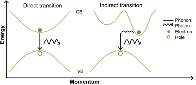
Figure 1.23. Schematic representation of the energy versus the momentum for the valence (VB) and
conduction bands (CB) of semiconductors and the difference between direct and indirect
transitions (or band gaps). ... 27
Figure 1.24. WO3 crystal structures, designed in CrystalMaker software for: a) Monoclinic (m-WO3) and
b) Hexagonal (h-WO3) configurations. ... 27
Figure 1.25. Crystal structure, designed in CrystalMaker software, for orthorhombic hydrated WO3
(ortho-WO3·0.33H2O). ... 28
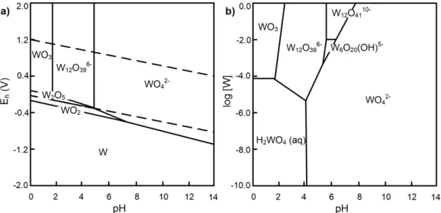
Figure 1.26. a) Pourbaix diagram for W-H2O system at 25 ºC and tungsten molar concentration of 10-4 M
(dashed lines represent the limits of stability of water), and b) Solubility diagram for a fixed
potential of Eh = 0.2 V, 25 ºC and 3 M ionic strength.[100]–[102] ... 29
Figure 1.27. Schematic representation of an electrochromic device, a) before and b) after charge
appliance (with the cation insertion and color modification of the electrochromic material). ... 30
Figure 1.28. Examples of electrochromic applications developed in CENIMAT: a) Electrochromic passive
matrix in paper, under the project SMART-EC (FP7-ICT-2009.3.9/258203), b) Transparent
electrochromic window, and c) Gas sensor prototype with EC display on paper, under the project
A3PLE (FP7-NMP-2010-SME/262782-2). ... 30
Figure 1.29. Schematic band structure of Ga2O3-In2O3-ZnO (filled states are colored). The energy band
gaps (Eg) are reported for crystalline structures.[127] ... 32
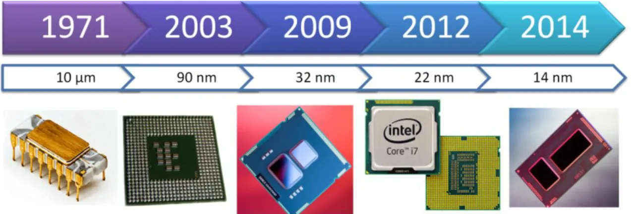
Figure 1.30. Evolution of the transistors’ size used in Intel processors during the last decades. ... 35 Figure 2.1. Schematic representation of the hydrothermal synthesis process. ... 46
Figure 2.2. a) SEM images and b) XRD diffractograms of the hydrothermal synthesized WOx
nanopowders, using PTA as precursor with three different synthesis acidities and times. Adapted
from [3]. ... 47
Figure 2.3. a) SEM images and b) XRD diffractograms of the hydrothermal synthesized WOx
nanopowders using Na2WO4 as precursor with three different synthesis acidities and times... 49
Figure 2.4. SEM images of the microwave assisted hydrothermal synthesized WO3 nanopowders using
Na2WO4 as precursor, Na2SO4 as structure directing agent, for 1 hour, with constant power of 100
W and at a) pH 1.8 and b) pH 0. ... 49
Figure 2.5. XRD diffractograms of the hydrothermal synthesized V2O5 xerogels with three different
synthesis times and using: a) 0.1 g, b) 0.05 g and c) 0.01 g of V2O5 powder as precursor. ... 50
Figure 2.6. a) SEM image of the hydrothermal synthesized V2O5 xerogel with 0.05 g of precursor and for
24 h and b) simulation of the m-V2O5 layered structure, performed in CrystalMaker software. .... 51
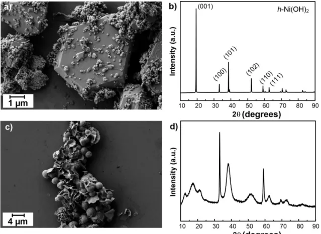
Figure 2.7. SEM image and XRD diffractogram of the hydrothermal synthesized hexagonal Ni(OH)2
powder from: a) and b) NiSO4, and c) and d) Ni(CH3COO)2 precursors. ... 52
Figure 2.8. a) SEM image and b) XRD diffractogram of the hydrothermal synthesized monoclinic HfO2
nanopowder. ... 53
Figure 2.9. a) SEM image and b) XRD diffractogram of the hydrothermal synthesized tetragonal -MnO2
nanowires. ... 53
Figure 2.10. a) SEM image and b) XRD diffractograms of the hydrothermal synthesized GIZO
xvi
Figure 2.11. a) SEM image and b) XRD diffractogram of the hydrothermal synthesized ZTO nanopowder.
... 55
Figure 3.1. a) XRD diffractograms of the nanopowders synthesized n: (a) H2O; (b) 0.3 M HCl and (c) 3 M
HCl. Reference diffractograms for ortho-WO3·0.33H2O (ICDD: 01-072-0199) and m-WO3 (ICDD:
43-1035) have been placed above; b) Graphic representation of the crystallographic structure of the
synthesized polymorphs (m-WO3 and ortho-WO3.0.33H2O) obtained using Crystal Maker®
software. ... 60
Figure 3.2. SEM images, EDS element distribution and TEM analysis of nanopowders obtained via
hydrothermal synthesis performed in: a) H2O; b) 0.3 M HCl and c) 3 M HCl. SEM images are false
colored for a better visualization of the nanostructures... 61
Figure 3.3. TG of nanopowders obtained via hydrothermal synthesis performed from in: a) H2O; b) 0.3 M
HCl and c) 3 M HCl ... 62
Figure 3.4. a) Impedance plot for the full frequency range. Nyquist plot of WOx nanopowders performed
at room temperature and their theoretical fit (red line) to a CPE circuit (inset) for: b) m-WO3 +
ortho-WO3.0.33H2O; c) ortho-WO3.0.33H2O; d) m-WO3 ... 64
Figure 3.5. a) UV/Vis absorbance spectra and the correspondent Tauc’s plots corresponding to: b) indirect and c) direct transitions of WO3 nanoparticles dispersed in water. ... 65
Figure 3.6. In situ transmittance measurements at 800 nm applying a potential of ± 2 V for 30 s of inkjet
dual-phase thin films: a) a-WO3/(m-WO3+ortho-WO3.0.33H2O); b) a-WO3/ortho-WO3.0.33H2O; c)
a-WO3/m-WO3 and d) single a-WO3 thin film. ... 66
Figure 3.7. Cyclic voltammograms of inkjet printed dual-phase thin films performed in an
electrochemical cell with platinum wire as counter electrode, Ag/AgCl as reference electrode in
lithium based gel electrolyte at a scan rate of 50 mV/s. ... 67
Figure 3.8. Stability of CV measurements of inkjet printed thin films for 1000 cycles for a potential range
from 0.5 to -1V. Capacity loss represents the charge difference between first and following cycles
obtained by the integration of the cyclic voltammogram. ... 69
Figure 3.9. Ex-situ lithiation study of a) ortho-WO3.033H2O and b) m-WO3 nanoparticles deposited on
ITO/glass substrates with 0.5 M LiClO4 in PC electrolyte. ... 70
Figure 4.1. Simplified schematics of the first pH device using a WO3 sensing layer. The device turns ON
(ID > 0) and OFF (ID = 0) depending on the oxidized (insulating) or reduced (conductive) states of
WO3, respectively. Similar effect is observed by varying the pH (adapted from the work published
by Wrighton et al.[22]). ... 79
Figure 4.2. Scheme of the: a) sensor production procedure, b) sensor design and structure and c)
photograph of the final fabricated sensor. ... 81
Figure 4.3. SEM image of WO3 nanoparticles. The inset shows a higher magnification of the
nanoparticles exhibiting nanoslabs-type shape agglomerates. ... 83
Figure 4.4. a) XRD diffractograms of WO3 synthesized powder and orthorhombic WO3·0.33H2O reference
pattern (the * peaks correspond to unidentified structure); b) Crystal structure simulation of
orthorhombic WO3·0.33H2O (produced in crystal maker software); c) FTIR spectrum and d)
Nitrogen adsorption-desorption isotherms of WO3 nanoparticles performed at standard
xvii
Figure 4.5. SEM images of: a) Sensing area after WO3·0.33H2O nanoparticles electrodeposition; b)
Cross-section overview of Ti/Au, electrodeposited WO3 nanoparticles and carbon sacrificial layers after
FIB milling (The image was colored for better understanding of the layered structure). ... 86
Figure 4.6. a) Calibration curve of transmittance values at 280 nm wavelength for WO3 dispersions of
different concentrations and b) Transmittance of the PBS solution after dipping the WO3 sensor at
37 ºC for 8 days. ... 87
Figure 4.7. Impedance modulus (solid lines) and phase angle (dashed lines) plots of the electrode before
and after WO3.0.33H2O nanoparticles electrodeposition. ... 88
Figure 4.8. pH sensitivity measured from pH 9 to 5 of: a) Au/WO3 nanoparticles electrodes; b) Au
electrode. The sensitivity is indicated inside the graphic. ... 89
Figure 4.9. Electrochemical potential behavior of the pH sensor during three completes cycles for pH
range of 9 to 5 and 5 to 9. ... 90
Figure 4.10. Electrochemical potential behavior of the electrode after dipping in buffer solution of pH 9,
7 and 5. The response time was calculated as the time necessary to reach 90% of the maximum
potential value. ... 92
Figure 4.11. a) pH sensitivity of WO3 sensor using a flexible Ag/AgCl reference electrode in a non-planar
surface made of gelatin-based electrolyte; b) photograph of the prototype. ... 93
Figure 5.1. Representation of the 3D structure of cytochrome c nitrite reductase, with the heme groups
coordinating a central iron atom (deep red spheres). ... 101
Figure 5.2. Left side: a) XRD patterns of hydrothermally synthesized WO3 powders; W1) 2.7 M, W2) 1.5
M and W3) 0.3 M of HCl (reference diffractograms for m-WO3, ICDD: 43-1035 and ortho
-WO3·0.33H2O, ICDD: 01-072-0199 has been placed at bottom), b) Representation of (002)
crystallographic plane projection (performed in crystal maker© software) for m-WO3 and c)
ortho-WO3·0.33H2O. Right side: SEM microstructures and TEM lattice-images of hydrothermal
synthesized WO3 nanoparticles: d), g) W1; e), h) W2; and f), i) W3. SEM images were false colored
for better visualization of the nanoparticles structure while the darker background corresponds to
the ITO electrode. The inset on TEM lattice-images shows the corresponding FFT images. The size
scales of SEM and TEM images are the same in the three samples. ... 104
Figure 5.3. Electrochemical characterization of ITO and WO3/ITO electrodes. a) Nyquist plots measured
with an alternative voltage of 10 mV and frequency range 1-106 Hz; b) cyclic voltammograms
performed at a scan rate 50 mV/s. The supporting electrolyte was 0.1 M KCl in 0.05 M tris-HCl pH
7.6 buffer. ... 107
Figure 5.4. Cyclic voltammograms of cyt c at ITO and WO3/ITO electrodes measured at variable scan
rates, from 35 to 750 mV s-1. Protein concentration was 0.2 mM in 0.1 M KNO
3,0.05 M phosphate
buffer pH 7.6., Inset: Variation of anodic and cathodic peak current as a function of the square
root of the scan rate. ... 109
Figure 5.5. Typical electrochemical response of ccNiR/WO3/ITO electrodes in response to variable nitrite
concentration (0-0.8 mM). a) Cyclic voltammograms performed at a scan rate of 50 mV s-1 in 0.05
M tris-HCl pH 7.6 buffer with 0.1 M KCl; b) Catalytic current (measured at -0.8 V) as a function of
nitrite concentration and fitting (solid line) of the experimental data to the Michaelis-Menten
xviii
Figure 6.1. a) Comparison of the cross section of an inorganic GIZO based nanoparticles transistor using
a conventional dielectric film and an electrolyte; b) Schematics of the voltage (V) and electric field
(E) distributions in a conventional dielectric and in electrolyte gate insulator when a positive gate
voltage is applied; c) Schematics of the transistors architecture for a conventional structure
incorporating thick gate dielectric (~100 nm) and for an EGT in which the gate dielectric is replaced
by a polymer electrolyte, with indication of both EDLs at the gate/electrolyte and
semiconductor/electrolyte interfaces. ... 127
Figure 6.2. a) XRD diffractograms before and after annealing at 900 ºC and reference ICDD
diffractograms of c-In2O3, m-Ga2O3 and h-ZnO (file numbers 06-0416, 41-1103 and 05-0664,
respectively); b) TEM image of GIZO nanoparticles before annealing (inset shows the diffraction
pattern of the nanoparticles). ... 131
Figure 6.3. SEM images: a) before and b) after FIB milling; c) –f) EDS mapping of the elements; g) EDS
spectrum and h) average of the atomic weights performed in 10 samples of GIZO (colored) and
their percentages before synthesis (blank). ... 132
Figure 6.4. AFM topographic and phase images of GIZO20 films annealed at: a) 250 ºC and b) 350 ºC. The
inset corresponds to the nanoparticles radius size distribution measured with the Gwyddion
software. ... 134 Figure 6.5. a) Impedance modulus (□), phase angle (○) and capacitance (Δ) plot from EIS measurement
(the inset represents the equivalent electric circuit, where R is the resistance, W the Warburg and
CPE the constant phase elements) and b) Cyclic voltammogram of ITO/electrolyte/ITO capacitor
structure at a scan rate of 50 mV/s. EIS conditions: alternative voltage 10 mV and frequency range
1-106 Hz. ... 135
Figure 6.6. Transfer characteristics, gate current with different gate voltage ranges (the red dashed line
corresponds to VG from -2 to 1 V and the solid black line from -2 to 2 V) and high resolution SEM
image, after FIB milling, of the cross-section of EGT built with: a) GIZO30 and b) GIZO20 after 1 h
annealing at 350 C. Transfer characteristics and gate current were measured with 0.5 s delay time
and the arrows represent the sweep direction. ... 138
Figure 7.1. Bitalino plugged kit, available at www.bitalino.com, as an example of a commercial wearable
sensor. ... 150
Figure S 3.1. a) SEM image of inkjet printed a-WO3/ortho-WO3.0.33H2O (detail of the pattern formed by
the a-WO3layer), b) Transmittance plots and c) Tauc’s plots for all inkjet printed thin films. ... 75
Figure S 3.2 Transmittance plots for all inkjet printed thin films in colored (2 V) and bleached (-2 V)
states, after applying a fixed potential for 60 s. ... 75
Figure S 4.1. Schematic and real image of the electrodeposition set-up composed by WO3 nanoparticles
dispersion in water, flexible gold working electrode, platinum wire as counter electrode and
Ag/AgCl as reference electrode. ... 97
Figure S 4.2. Impedance modulus and phase angle of the flexible reference electrode after anodization
of the Ag layer and saturation in KCl solution. ... 97
Figure S 5.1. Schematic representation of the set-up used in electrochemical characterization; composed
by a WO3/ITO working electrode, buffer electrolyte, platinum wire as counter electrode and
xix
Figure S 5.2. Raman spectra obtained from the samples W1, W2 and W3 at RT with 413 nm laser
excitation, 6.5 mW laser power and 30 s accumulation. ... 120
Figure S 5.3. Nyquist plots of: a) WO3 pellets performed at RT between two gold flat electrodes and b)
WO3/ITO electrodes performed in 0.05 M tris-HCl pH 7.6 buffer with 0.1 M KCl as electrolyte. The
alternative voltage was of 10 mV and the frequency range between 1-106 Hz. The theoretical
fitting is represented by the solid lines. ... 120
Figure S 5.4. Representation of the drop casting method for the preparation of the WO3/ITO electrodes.
... 121
Figure S 5.5. Cyclic voltammograms of ITO and WO3/ITO electrodes in 1 mM [Fe(CN)6]4-/3- solution at
variable scan rate, from 10 to 250 mV/s (insets correspond to the plots of peak current vs. square
root of scan rate). ... 121
Figure S 5.6. Resonance Raman spectra of ccNiR immobilized in WO3/ITO electrodes, measured with 413
nm excitation, 1.2 mW laser power and 5 s accumulation time, at RT. Each spectrum represents a
sum of 5 individual spectra. ... 122
Figure S 6.1. Schematic representation of the semiconductor (green)/electrolyte (blue) interface when a
positive gate voltage is applied, considering: a) electric double layer and b) electrochemical
operation modes. ... 142
Figure S 6.2. Final transistor structure with top gate, electrolyte and GIZO nanoparticles as
semiconductor... 143 Figure S 6.3. Tauc’s plot for GIZO nanoparticles dispersion. ... 144 Figure S 6.4. a) DLS size distributions and b) DSC-TG curves performed in air up to 600 ºC, for the two
GIZO inks after filtration. ... 145
xx
List of Tables
Table 1.1. Resume of the latest research on nanostructured EC oxides, deposition methods, optical
modulation (Tmax), applied potential, coloration (col) and bleaching (bl) times, and coloration
efficiency (CE). ... 34
Table 3.1. Comparison of nanoparticles sizes from SEM images and DLS hydrodynamic diameter, BET
surface areas and fitted bulk conductivity calculated from Nyquist plots of WO3 pellets. ... 63
Table 3.2. Optical densities (OD), charge ratio (Qratio) and coloration efficiency (CE) of inkjet printed thin
films. ... 68
Table 4.1. Relative cell viabilities after 24, 48 and 72 hours of incubation of the cells with conditioned
media. ... 85
Table 4.2. Electrochemical potential values of three WO3 sensors measured from pH 9 to 5 and
corresponding sensitivity... 90
Table 4.3. Electrochemical potential values for the same WO3 sensor measured from pH 9 to 5 and 5 to
9, during three complete cycles and the resulting sensitivity. ... 91
Table 5.1. Comparison of nanoparticle sizes measured by SEM and DLS techniques along with BET
surface areas and fitted bulk conductivity calculated from Nyquist plots of the 3 samples. ... 105
Table 5.2 Electrochemical parameters of cytochrome c on different WO3/ITO electrodes (anodic and
cathodic peak current ratio (Ic/Ia), peak separation (Ep), formal redox potential (E0), diffusion
coefficient (D0) and heterogeneous exchange rate constant (k0)), as obtained by cyclic
voltammetry, in 0.05 M phosphate buffer, pH 7.6, 0.1 M KNO3, at variable scan rates (from 35 to
750 mV s-1). ... 109
Table 5.3. Comparison of the kinetic and analytical parameters of the bioelectrode configurations tested
in this work with previously reported amperometric or voltammetric biosensors also based on
ccNiR from D. desulfuricans. Michaelis-Menten constant (KM); limit of detection (LOD); linear range
and sensitivity. PG: pyrolytic graphite; SWCNT: single-walled carbon nanotubes; MWCNT:
multi-walled carbon nanotubes; CPSPE: carbon paste screen-printed electrode; ND: not determined; R2:
correlation coefficient. ... 112
Table 6.1. Key factors of the reported work for EGTs with metal oxide nanoparticles: deposition
technique, post-treatment, electrolyte, channel width to length ratio (W/L), on-off current ratio
(ION/IOFF), threshold voltage (VTh), drain voltage (VD), mobility (µ) and sub-threshold swing (SS). . 128
Table 6.2. Resume of the electric characterization of the produced EGTs: channel weight and length
ratio (W/L), drain voltage (VD), gate current range (VG), on-off current ratio (ION/IOFF), threshold
xxi
Abbreviations
0D Zero dimensions
1D One dimension
2D Two dimensions
3D Tree dimensions
aq. Aqueous
a- Amorphous
AC Alternating Current
AFM Atomic Force Microscope
BET Brunauer-Emmet-Teller
c- Cubic
CB Conduction Band
ccNiR Cytochrome c nitrite reductase
CE Coloration Efficiency
CENIMAT Materials Research Center
CSPE Composite Solid Polymer Electrolyte
CV Cyclic Voltammetry
Cyt c Cytochrome c
DL Diffusion Layer
DLS Dynamic Light Scattering
DLVO Derjaguin-Landau-Verwey-Overbeak
DMSO Dimethyl Sulphoxide
EC Electrochromic
ECT Electrochemical Transistor
EDL Electric Double Layer
EDLT Electric Double Layer Transistor
EDS X-Ray Spectroscopy
EGT Electrolyte-gated Transistor
EIS Electrochemical Impedance Spectroscopy
FIB Focused Ion Beam
FTIR Fourier Transform Infrared Spectroscopy
GIZO Gallium-Indium-Zinc-Oxide
h- Hexagonal
i3N Institute of Nanostructures, Nanomodelling and Nanofabrication
IBM International Business Machines
ICDD International Center for Difraction Data
xxii ISFET Ion Sensitive Field Effect Transistor
ISO Internation Standard Organization
ITO Indium-Tin Oxide
IZO Indium-Zinc Oxide
LSW Lifshitz-Slyozov-Wagner
m- Monoclinic
M Metal
MRI Magnetic Ressonance Imaging
MWCNTs Multi-wall Carbon Nanotubes
ortho- Orthorhombic
O Oxygen
OHP Outer Helmholtz Plane
PBS Phosphate Buffer Solution
PC Propylene carbonate
PET Polyethylene Terephthalate
PTA Peroxopolytungstic Acid
PTFE Polytetrafluoroethylene (Teflon)
PZC Point of Zero Charge
QD Quantum Dot
R Organic group
rpm Rotation per minute
RR Ressonance Raman
RT Room Temperature
S:V Surface to volume ratio
SEM Scanning Electron Microscopy
STM Scanning Tunneling Microscopy
STP Standard Temperature and Pressure
t- Tetragonal
TEM Tunneling Electron Microscopy
TFT Thin-film Transistor
TG Thermogravimetry
UV Ultraviolet
UV/vis Ultraviolet-visible
VB Valence Band
WOx Tungsten Oxide
xDLVO Extended Derjaguin-Landau-Verwey-Overbeak
XRD X-Ray Diffraction
xxiii
Symbols
a Absorption Coefficient bl Bleaching Time col Coloration Time F Fermi Level
Ep Peak Potential Separation G Free Gibbs Energy
G* Energy barrier for the formation of the nuclei of the nanoparticle GS Surface Free Energy
Gv Volume Free Energy OD Optical Density
T Optical Modulation
Surface Energy per unit area µ Mobility
µFE Field-effect Mobility
µLIN Linear Mobility
µSAT Saturation Mobility
Conductivity
A Hamaker constant
CDL Double Layer Capacity
CS Equilibrium Solubility
Cnucleation
min Minimum Solubility for Nucleation Cnucleation
max Maximum Solubility for Nucleation D0 Diffusion Coeficient
E0 Formal Redox Potential
Eg Band Gap Energy
eV Electron Volt
G Gibbs Energy h Photon energy
I Current
Ic/Ia Anodic and Cathodic Peak Current Ratio
Icat Catalytic Current
Imax Catalytic Current observed at the maximum turnover rate
ION/IOFF On-off Current Ratio
xxiv k0 Exchange Rate Constant
KM Michaelis-Menten Constant
l Thickness
Qratio Charge Ratio
Qi Charge Intercalated
Qdi Charge Deintercalated
r Nanoparticle Nuclei Radius
r* Minimum Nuclei Size for a Stable Nanoparticle
R Reflectance
R2 Correlation coefficient
Re Electrical Resistance
Rs Solution Resistance
SS Subtreshold Swing
T Transmittance
Tbl Transmittance in the Bleached State
Tcol Transmittance in the Colored State
VA Attractive Forces
VD Drain Voltage
VG Gate Voltage
VR Repulsive Forces
VT Total Potential Energy
VTh Threshold Voltage
W/L Width to Length Ratio
Y0 Bulk Resistance
Z Impedance
Zimag Imaginary part of the Impedance (Z’’)
Zreal Real part of the Impedance (Z’)
Zphase Impedance Phase
1
Chapter 1.
INTRODUCTION
2
1.1.
Nanoscience and Nanotechnology
Nanoscience and nanotechnology became a distinguishable and multidisciplinary field of re-search with emerging applications. It is one of the most visible and growing rere-search areas in science and technology and, all over the world research funding agencies have been supporting the exploitation of the potentialities of this field in the areas of chemistry, materials, engineering and medicine. Nanoscience and nanotechnology are fueling a new industrial revolution supported by the scientific ability to fabricate, model and manipulate objects with a small numbers of atoms, and the almost daily discovery of new phenomena at the nanoscale.[1], [2]
The term “nanotechnology” has first appeared in a conference in 1974 by Norio
Tanigu-chi,[3] but the idea of building “small” things is usually attributed to Richard Feynman based on the talk he gave in 1959, where he predicted that machines would build even smaller machines and other products with atom by atom control, a process which was later called molecular manu-facturing.[4] Truthfully, interfaces and colloids science existed for nearly a century before they became associated with nanotechnology. The first observations and size measurements of na-noparticles have been performed in the beginning of 20th century by Richard Zsigmondy, winner
of the 1925 Nobel Prize in Chemistry for his demonstration of the heterogeneous nature of colloid solutions and for the methods he used, which have since become fundamental in modern colloid chemistry.[5], [6] Zsigmondy was also the first to use the term “nanometer” explicitly for charac-terizing particle sizes. At the same time, Irving Langmuir, winner of the 1932 Nobel Prize in Chem-istry introduced the concept of a monolayer, a layer of material with one molecule thick.[7]
Later on, the major boost to further develop the nanotechnology was achieved in 1981 by Gerd Binnig and Heinrich Rohrer at IBM Zurich Research Laboratory with the invention of the scanning tunneling microscope (STM), for which they were awarded with the Nobel Prize in Phys-ics in 1986,[8] and in 1985 Binnig, Calvin Quate and Christoph Gerber invented the atomic force microscope (AFM).[9] At this time (1985), the first fullerene was discovered by Harry Kroto, Rich-ard Smalley and Robert Curl, who together won the 1996 Nobel Prize in Chemistry.[10] The dis-covery of carbon nanotubes even if generally attributed to Sumio Iijima due to the impact of his
“Nature” paper in 1991,[11] was first published in 1952 by L. V. Radushkevich and V. M. Lukya-novich, but in Russian language.[12] Still in 1986, Eric Dexter published the book “Engines of Creation” and he is described as the founding father of nanotechnology. He established main fundamentals of molecular engineering and described the implementation and applications of advanced nanotechnologies.[13] Drexler was also one of the co-founders of the Foresight Insti-tute that is: “the primary force pushing for the kind of nanotechnology that will truly transform our future, from medicine to the environment to space settlement”.[14]
3
New University of Lisbon) and FSCOSD (Physics of Semiconductors, Optoelectronics and disor-dered Systems, hosted by the University of Aveiro).
In 2013, IBM launches “A Boy and His Atom: The World’s Smallest Movie” in which the
atoms are moved by using their STM and recorded in a movie to further promote IBM’s research in the field of atomic-scale memory and to reveal the latest developments and new possibilities in nanotechnology. [15]
Figure 1.1 depicts the major events related with nanoscience and nanotechnology.
Figure 1.1. Major historic events for the development of nanoscience and nanotechnology.
4
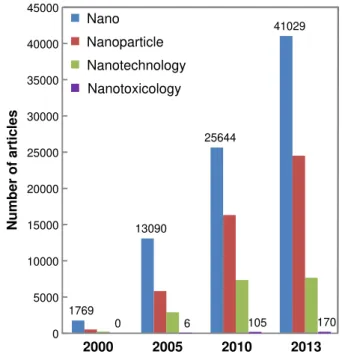
Figure 1.2. Number of manuscripts published in 2000, 2005, 2010 and 2013 under the topics: Nano, Nanoparticle, Nanotechnology and Nanotoxicology. Based on topic search performed in ISI web of knowledge, at Dec. 2014.
The main reason for the fascination in nanostructures is their interesting properties, which are not found in the bulk materials. Surface and quantum effects arise in nanostructures due to the large surface-to-volume (S:V) ratio and to the dimensions that are comparable to the electron wavelength, respectively.[16]
1.2.
Nanomaterials
Nanostructured materials (nanomaterials) include atomic clusters, layered or lamellar films, fila-mentary structures, and bulk nanostructured materials. The common thread to these various ma-terial forms is the nanoscale dimensionality, i.e. at least one dimension less than 100 nm.[1] This systems can be classified as 0D if the system exhibits a nanometric size in the three spatial dimensions, 1D if the nanometric size is in two dimensions or 2D systems if one spatial dimension is nanometric. Bulk nanostructured materials are classified as 3D systems. In solid-state physics and optoelectronics 0D, 1D and 2D structures are usually named quantum dots, quantum wires and quantum wells, respectively (Figure 1.3). However, the interest for this kind of systems is not restricted only to these scientific fields since confined structures are also widely employed in ca-talysis, energy storage applications, thermoelectric materials, photocaca-talysis, mechanical met-amaterials and biotechnology.[17] Structural geometry of nanostructures becomes more compli-cated in the case of composite and multi-component materials. Categories of nanocomposites consisting of a minimum of two phases (with at least one phase having sizes less than 100 nm), are specified by the size scales and geometry of the constituent phases.
1769
13090
25644
41029
0 6 105 170
0 5000 10000 15000 20000 25000 30000 35000 40000 45000
2000 2005 2010 2013
5
Figure 1.3. Nanomaterials classification according to its dimensionality.
Surfaces and interfaces are also important in explaining nanomaterial behavior. In bulk materials, only a relatively small percentage of atoms will be at, or near, a surface or interface. In nanomaterials, the small feature size ensures that many atoms, perhaps half or more in some cases, will be near interfaces. Surface properties such as energy levels, electronic structure, and reactivity can be quite different from interior states, and give rise to different material properties.[1]
In fact, as highlighted above, their peculiar dimensionality gives rise to quantum confine-ment phenomena, which modify the structural, optical, chemical and electronic properties with respect to the corresponding bulk materials. For instance, systems with different dimensionalities show significantly different optical properties, which arise from their peculiar density of states (Figure 1.4). A bulk material exhibits a square root energy (E1/2) dependence of the density of
states, while in 2D system is described by a step function, the 1D systems show a E−1/2
depend-ence for each quantized state, and in 0D, all available states exist only at discrete energy values since the electron is confined in all three spatial dimensions.[17], [18]
6
Figure 1.4. Electronic density of states for a bulk 3D, 2D, 1D nanocrystalline material and 0D quantum dot. The arrows represent the spatial confinement occurring in each system.
7
Figure 1.5. a) Nanotechnology consumers’ products evolution; b) Most common materials used in the products; and c) Products categories. The inventory was performed in October 2013.[21]
a)
b)
8
In the field of medicine and biology, several nanoparticle applications have already been approved for clinical use, and many others are at different stages of development. Nanoparticle-based biomedical applications include drug delivery, tissue engineering, fluorescent biological labeling, and magnetic ressonance imaging (MRI) contrast enhancement.[22]
As discussed before, the extraordinary optical, mechanical, electrical, and chemical prop-erties of the nanomaterials are highlighted in some of the major breakthroughs of this field:[23]
1) Magnetic nanoparticle assemblies that present novel magnetic properties with respect to their bulk constituent components due to surface effects produced by the modified atomic symmetry, in such, low dimensional systems and magnetic coupling between the parti-cles.
2) The combination of low toxicity, high surface area, biocompatibility, and colloidal stability of gold nanoparticles allowed the its integration into biosensors. The use of nanomaterials and their composite results not only on a stable immobilization matrix (in the electrode surface) but also act as catalyst for many reactions, thus resulting in enhanced signal response.
3) The luminescence emission and absorption edge that were tuned by changing the parti-cle size and by controlling the defect chemistry of ZnO nanostructures (photocatalyst).
4) Nanohybrid materials formed between conducting polymers, and inorganic oxides with carbon nanotube that demonstrate an excellent solar energy conversion capacity. This resulted in a dramatic increase in the surface area and increase in electronic conductivity, and electrolyte accessibility of the nanoporous structure, which improved the perfor-mance of the nanohybrid photoanode and cathode as a solar energy extraction material. These results on nanocomposites also suggested that nanoporous composites of multi wall carbon nanotubes (MWCNTs) with conducting polymers are promising for energy conversion devices such as biosolar cells and QD sensitized solar cells.
1.3.
Nanoparticles Engineering
9
Figure 1.6. SEM images of: a) Diatom Frustule (image copyright © Dennis Kunkel Microscopy, Inc.), b) Diatom Coscinodiscus wailesii algaes (adapted from [28]), c) Swallowtail butterfly (image copyright © Dennis Kunkel Microscopy, Inc.), and d) Lycaenid butterfly wing scales (adapted from [29]).
Depending on the application, the most important features of the engineered nanomaterials are the chemical composition and the structural properties (size, morphology, crystallinity and crystallography). Therefore, the synthesis method should selectively yield the desired particle’
properties, and in large quantities. Following to the production of the nanoparticles, generally
there is the need to produce a dispersion that preserves the material’ properties with a good
quality and homogeneity. Stable dispersions are ideally achieved without the addition of a disper-sant, however, it is extremely difficult to attain it as the nanoparticles tend to agglomerate fairly quickly.[30] Hence, it is of great importance to fully understand the mechanism of the stability of the dispersion.[1]
1.3.1. Dispersions Stability
Nanoparticles aggregation and stability is mostly explained using the colloid science principles, based around Derjaguin-Landau-Verwey-Overbeak (DLVO) theory.
According to classical DLVO theory, the aggregation of nanoparticles is determined by the sum of the van der Waals attractive and electrostatic double layer repulsive forces.[31]
Since the potential energy due to the van der Waals attraction forces (VA) and to the
10
𝑽𝑨= −𝟏𝟐𝑨 [ 𝟒𝒓 𝟐
𝒄𝟐−𝟒𝒓𝟐+𝟒𝒓
𝟐
𝒄𝟐 + 𝟐𝒍𝒏 (𝒄 𝟐−𝟒𝒓𝟐
𝒄𝟐 )] (1.1)
𝑽𝑹=𝜺𝒑𝟖𝒓[𝟐𝚭𝟏𝚭𝟐𝒍𝒏 (𝟏+𝒆 −𝑲𝒄
𝟏−𝒆−𝑲𝒄) + (𝚭𝟏𝟐+ 𝚭𝟐𝟐)𝒍𝒏(𝟏 − 𝒆−𝟐𝑲𝒄)] (1.2)
where A is the Hamaker constant and is a material property,[33] r is the particle radius, c the
center-to-center distance between two interactive particles, p is the electrical permittivity, the
zeta potential of the two particles and K is the Debye-Huckel function,[34] then, the total potential
energy, given by DLVO theory, can be described as:
𝑽𝑻= 𝑽𝑨+ 𝑽𝑹 (1.3)
and is represented in Figure 1.7.
Figure 1.7. Electrostatic double layer (EDL), van der Waals and Derjaguin-Landau-Verwey-Overbeak (DLVO) forces represented as total potential energy as a function of nanoparticles separation distance.
The total potential energy presents two minima values depending on the separation dis-tance between the nanoparticles. These regions are characterized by flocculation (aggregated material that can be re-dispersed by agitation and sonication) and coagulation (irreversible ag-gregation of the material) that occur at larger and smaller particle separations, respectively (Fig-ure 1.7).
Depending on the assumptions taken by the authors, the equations 1.1 and 1.2 can be derived in simpler equations. For example, when the separation distance between two particles is much lower than its radius (c<<r), then VA can be simplified to:[35]
𝑽
𝑨= −
𝟏𝟐𝒉𝑨∙𝒓 (1.4)for spherical particles, where h is the separation distance between two interactive particle
sur-faces, or to:[1],[36]
𝑽
𝑨= −
𝟏𝟐𝝅𝒉𝑨 𝟐 (1.5)T o ta l p o te n ti a l e n e rg y Separation distance DLVO
EDL repulsion forces
11
for plate-shaped particles. With this assumption, it is clear the dependence of the attractive po-tential energy with the shape of the particle, and for spherical particles the decays of the energy with the separation distance is slower than for plate-shaped particles. This slower decay can be explained by the fact that at short distances, only part of the spheres are close together. A small change of the distance between the spheres has a substantial effect on the points of closest approach, whereas the bulk of the spherical nanoparticle maintains its properties constant.[36]
The electrostatic repulsive forces are dependent of the charge on the particle surface (equation 1.2). In the case of hydrous oxides in aqueous solutions, the OH− groups at the surface
of the particles can protonate (and deprotonate) depending on the pH of the solution. This process result in the creation of a charge on the particle surface according with the following equations:
M–OH + H+→M–OH
2+ (1.6)
M–OH + OH−→M–O− + H2O (1.7)
The pH at which the charge on the particle is zero is called the “point of zero charge” (PZC), and is a property of the material. At pH < PZC, the particle is positively charged while for pH > PZC, the charge of the particle is negative (Figure 1.8).[37]
Figure 1.8. Representation of the surface charge dependence with the pH.
The surface charge of the particle attracts ions (known as counterions) of opposite charge in the solution. These counterions bind to the particles via van der Waals and electrostatic forces. The water molecules are also attracted towards the surface charge and are held by van der Waals forces as well as by hydrogen bonds. Hence, the particle surface charge is screened by the coun-terions and create an electrical double layer (EDL). This EDL, associated with every colloidal particle, is responsible for generating a repulsive force between two neighboring particles, thus avoiding flocculation of particles (electrostatic stabilization).
The EDL (Figure 1.9) is formed by three distinct regions: inner Helmholtz plane, outer Helmholtz plane and diffuse layer. The first region consists in the adsorbed ions on the surface, the second the solvated ions in contact with the surface and the diffuse layer is composed of ions attracted to the surface of the particle via electrostatic forces and is dependent of the ions con-centration in the bulk of the electrolyte. For high ion concon-centration, the contribution of the diffuse layer and adsorbed ions to the EDL can be neglected. In this case, the EDL is determined by the
Su rf ace ch arg e pH 0 +
-Point of zero charge (PZC) M–OH + H+ → M–OH
2+
12
solvated ions, which are usually considered as being confined in a region with a thickness of 1 nm.[38], [39] This model was later symplified by Stern, to only two layers: Stern and diffuse layers. His theory states that ions have a finite size, so cannot approach the surface closer than a few nanometers. The first ions of the EDL are not at the surface, but at a distance d away from the
surface that is usually taken as the radius of the ion. Stern also assumed that some of the ions are specifically adsorbed by the surface of the particle, and this layer has became known as the Stern layer.[32]
Figure 1.9. Schematic representation of the electrical double layer (EDL) structure.
Small variations in the electrolyte concentration are known to change the characteristics of the EDL of the nanoparticles and hence affect the repulsive forces. This change in the stability of the dispersions can occur with only minor external changes and should be controlled during na-noparticles suspension.[40], [41]
Though, engineered nanoparticles challenge the limits of colloid science due to its variable shape, size, structure, composition, and presence of adsorbed or grafted organic molecules.[41] Consequently, researchers all over the world are continuously discovering new evidences and theories to further understand this mechanism, mainly using computer modeling.[42],[43]
Although nanoparticles dispersions are most commonly stabilized by the EDL of the parti-cles, it is also possible to prevent coagulation by using a thick adsorbed layer, which constitutes a steric barrier (Figure 1.10). The most common strategy to create an effective barrier is by ad-sorbing a polymeric layer on the nanoparticle surface where the following requirements should be fulfilled:
the surface of the nanoparticle should be completely covered with the polymer (to prevent polymer chains from attaching to two particles simultaneously);
the polymer should be firmly anchored to the surface of the nanoparticle so that it is not displaced during Brownian collisions;
the layer must be thick enough (typically >3 nm) to keep the point of closest approach outside the range of the attractive van der Waals forces;
+ -+ +
-+ + + -+ + + + +
-Inner Helmholtz plane
Outer Helmholtz plane Diffuse layer Nanoparticle
13
the non-anchored portion of the polymer must be well solvated by the liquid.
Figure 1.10. Representation of electrostatic and steric stabilization between two nanoparticles.
The adsorbed layer of the polymer prevents coagulation of the particles in two ways: en-tropicly and enthalpicly. When the two particles approach each other, the adsorbed layers over-lap, resulting in a decrease in the degree of motion of the polymer chains. This is the entropic contribution of the adsorbed polymer against the particle coagulation. As the particles approach each other, the solvent molecules, which surround the particles, are squeezed out. However, an osmotic pressure is created that tends to suck the liquid back into the space between the particles. This increases the energy required for the particles’ approach and it is the enthalpic contribution. The block polymers are particularly effective steric barriers in this respect, because one end can be made to be strongly adsorbed at the particle surface, while the rest of the chain can be tailored to have a high affinity for the solvent. The higher the affinity of the solvent for the polymer, the greater the enthalpic contribution to the stabilization.[1],[37]
Steric repulsion forces resulting from adsorbed polymer, polyelectrolyte coatings or natural organic matter makes the total potential energy to have only one minimum. Coated nanoparticles may therefore aggregate reversibly, which has significant consequences regarding the fate, transport, bioavailability, and effects of nanoparticles in the environment. In addition to steric re-pulsion forces, also bridging, osmotic, hydrophobic Lewis acid-base, and magnetic forces have been applied to match experimental data of various types of aggregating particles. These addi-tional forces are collectively known as the extended DLVO (xDLVO) theory and is represented in Figure 1.11.[41]
Figure 1.11. Extended Derjaguin-Landau-Verwey-Overbeak (xDLVO) forces represented as the total potential energy as a function of the nanoparticles separation distance.
T
o
ta
l
p
o
te
n
ti
a
l
e
n
e
rg
y
Separation distance
xDLVO
14
The relevant force type depends on the system tested, and frequently more than one xDLVO force is important. Moreover, forces are not completely independent of one another. In the case of nanomaterials, understanding aggregation using a DLVO- or xDLVO-based theory presents many challenges.
1.3.2. Synthesis Techniques
The techniques used to engineer nanoparticles are usually divided into mechanical milling, phys-ical processing, biologphys-ical processing and chemphys-ical processing. Nevertheless, the development of new fabrication and processing technologies, along with a fundamental understanding of the relationship between the structure and properties of the feedstock powders created, and contin-ues to create, a variety of possibilities to produce nanostructured materials not only as powders but also in films, composites and coatings.[1]
Mechanical milling (or mechanical attrition) involves grinding a large piece of material into small particles (Figure 1.12). A very high energy input is required to produce small nanoparticles with this method, and it is difficult to manufacture particles with uniform size and shape. The significant advantage of this method is that it can be readily implemented commercially.[1] This
“top down” approach is dependent of the gridding ball size and the dispersion medium used in
the milling, with no possibility to control the crystallographic structure.
Figure 1.12. a) Example of a ball mill from RETSCH[44], b) Typical containers and balls used in the equipment and c) Schematic representation of the ball milling process.
15
Figure 1.13. Representation of the most common physical processes used in nanostructures production.
In biological systems, shape controlled synthesis of nanomaterials is achieved either by growth in constrained environments such as membrane vesicles or through functional molecules such as poly-peptides that bind specifically to crystallographic planes of inorganic sur-faces.[51][52] By adapting biological specificity to materials synthesis and functionality, genera-tion of structures of controlled composigenera-tion, size, and shape can be achieved for technologically important applications ranging from plasmonics and biomedical devices to energy technolo-gies.[53] Nevertheless, the specificity of this systems require special equipment and usually re-sults in an expensive procedure.
In chemical processing, precursors and solvents in liquid or gas form are used to produce nanoparticles. These methods can require expensive chemicals, result in partly contaminated particles, and create significant amounts of chemical waste. Nevertheless, the strength of chem-istry in materials science is its versatility in designing and synthesizing new materials, which can be processed and fabricated into final products. Chemical synthesis permits the manipulation of matter at the molecular level which allows good chemical homogeneity. Also, by understanding the relationship between how matter is assembled on an atomic and molecular level and the material macroscopic properties, molecular synthetic chemistry can be tailor designed to prepare novel starting components. Better control of the particle size, shape, and size distribution can be achieved in particle synthesis. To benefit from the advantages of chemical processing, an under-standing of the principles of crystal chemistry, thermodynamics, phase equilibrium, and reaction kinetics is required.[30], [54] Chemical preparation of nanoscale particles with desired material properties is a “bottom-up” manufacturing approach and the most common chemical processes are exposed below.
1.3.2.1. Sol-gel
The synthesis of oxide nanoparticles by this procedure is based upon the hydrolysis and conden-sation/dehydration of metal alkoxide M(OR)n, where M is the metal, O is the oxygen and R is the

![Figure 1.16. Dielectric constant of water as a function of the temperature.[60]](https://thumb-eu.123doks.com/thumbv2/123dok_br/16694148.743755/45.892.289.677.129.420/figure-dielectric-constant-water-function-temperature.webp)
![Figure 1.19. a) Plot of LaMer model for the generation of atoms, nucleation, and subsequent growth of colloidal synthesis;[67] b) Representation of Gibbs free energy variation for nucleation as function of the radius of the solid cluster;[70] c) Sche](https://thumb-eu.123doks.com/thumbv2/123dok_br/16694148.743755/49.892.247.688.123.989/generation-nucleation-subsequent-colloidal-synthesis-representation-variation-nucleation.webp)