2016
José Miguel
Alves Faria Gomes
Characterization and Modelling of Long-Term
Memory Effects in GaN HEMTs
Caracterização e Modelação de Efeitos de Memória
Lenta em Transístores GaN HEMT
2016
José Miguel
Alves Faria Gomes
Characterization and Modelling of Long-Term
Memory Effects in GaN HEMTs
Caracterização e Modelação de Efeitos de Memória
Lenta em Transístores GaN HEMT
Dissertação apresentada à Universidade de Aveiro para cumprimento dos requisitos necessários à obtenção do grau de Mestre em Engenharia Eletrónica e de Telecomunicações, realizada sob a orientação científica do Doutor José Carlos Esteves Duarte Pedro, Professor Catedrático no Depar-tamento de Eletrónica, Telecomunicações e Informática da Universidade de Aveiro e sob a co-orientação científica do Doutor Pedro Miguel da Silva Cabral, Professor Auxiliar no Departamento de Eletrónica, Telecomu-nicações e Informática da Universidade de Aveiro
Presidente / President Prof. Dr. João Nuno Pimentel da Silva Matos Professor Associado da Universidade de Aveiro (presidente)
Vogais / Examiners committee
Prof. Dr. José Carlos Esteves Duarte Pedro
Professor Catedrático da Universidade de Aveiro (orientador)
Prof. Dr. João José Lopes da Costa Freire
os estudos. Quero manifestar também a minha gratidão pelo seu esforço, dedicação e trabalho diários que, sendo o maior exemplo que me puderam dar, permitiram que eu pudesse percorrer o caminho que me trouxe até este momento.
Em segundo lugar, agradeço à minha irmã, Ana Sofia, pelos seus sábios e avisados conselhos e sobretudo porque o seu exemplo é um modelo para mim. Também ao meu cunhado, Luís Rafael, pelo seu exemplo e dedicação. Deixo também um agradecimento especial a duas pessoas que, mesmo não podendo ler este documento, foram, são e serão para mim uma fonte de alegria e motivação, a minha avó, Maria de Jesus, porque foi uma segunda mãe para mim e a minha sobrinha e afilhada, Maria Margarida, pela sua simples existência.
Quero também agradecer a todos aqueles que contribuiram directa ou in-directamente para a realização deste trabalho. Em particular ao professor José Carlos Pedro, pela paixão e sabedoria que evidencia quando transmite o seu conhecimento e experiência, sobretudo a nível técnico-científico, mas não só. Um agradecimento também ao professor Pedro Cabral pela sua co-orientação neste trabalho. Não posso deixar de mencionar também o doutor Luís Nunes e o senhor Paulo Gonçalves, pelas opiniões e sugestões que me ofereceram durante a execução do trabalho experimental.
Por fim, uma palavra especial para todos aqueles que encontrei ou re-encontrei durante a conclusão deste trabalho no Instituto de Telecomu-nicações. Muito obrigado a todos pelo apoio.
de Armadilhamento de Electrões
Resumo A tecnologia GaN HEMT tem revolucionado o mercado dos amplificadores de potência para RF. O seu potencial, comparado com tecnologias an-teriores, como a Si LDMOS, continua por ser completamente explorado. Contudo, a falta de uma boa caracterização e modelação dos efeitos de memória lenta causados pelo armadilhamento de cargas têm impedido o to-tal aproveitamento desta tecnologia no desenho de amplificadores de potên-cia. Consequentemente, estes fenómenos de armadilhamento têm sido alvo de um amplo estudo tanto a nível científico como industrial. Isto deve-se, so-bretudo, porque a linearidade dos amplificadores baseados nesta tecnologia é bastante afectada pelo estado de armadilhamento de cargas no disposi-tivo, que, por sua vez, é definido pela tensão de pico na saída, drain, do transístor. As ferramentas de desenho de circuitos auxiliado por computa-dor estão presentes na maioria dos laboratórios de investigação. No entanto, estas dependem não só dos seus algoritmos de simulação mas também, em larga medida, dos modelos nelas utilizados, tornando fundamental o desen-volvimento de melhores modelos.
O presente documento descreve a extracção de um modelo de circuito equiv-alente de pequeno signal dependente da polarização, de um transístor GaN HEMT de 3.3 W, a partir de medidas de parâmetros-S pulsadas, assim como a construcção de um sistema de medidas pulsadas DC I-V e a utilização deste último na caracterização de efeitos de armadilhamento. O sistema de-senvolvido, baseado em dois circuitos pulsadores desenhados para medidas pulsadas quer no terminal de entrada, gate, quer no de saída, drain, foi au-tomatizado através do software MATLAB instalado num PC. Os circuitos pulsadores permitem larguras de pulso na escala dos microsegundos com
duty-cycles tão pequenos como 0.001%, assim como, elevadas tensões de
saída - perto de 50 V - e correntes - pelo menos até 4 A. Com o sistema desenvolvido, obtiveram-se curvas I-V iso-térmicas e também curvas I-V iso-dinâmicas, dependentes do estado de armadilhamento, de um transístor GaN HEMT de 15 W. De modo a obter as últimas, foram utilizadas medidas de duplo-pulso. A assimetria esperada nas constantes de tempo associadas com o drain-lag foram claramente observadas: na escala dos ns para o ar-madilhamento e das centenas de milisegundos para o desarar-madilhamento. Tal como a literatura prevê para tecnologias mais recentes de GaN HEMTs, o impacto dos fenónemos de gate-lag que foi observado revelou-se bastante reduzido.
Abstract Gallium nitride (GaN) high electron mobility transistor (HEMT) technol-ogy has been revolutionizing the RF power amplifier (PA) market. Its po-tential, versus existing technologies, such as Silicon (Si) Laterally-Diffused MOS(LDMOS), is yet to be completely explored. However, the lack of good characterization and modelling of charge carrier trapping related phenom-ena has been hampering PA designers from extracting this technology’s promised performance. Hence, GaN HEMT trapping has been given a great amount of attention by the scientific and industrial worlds. This is mainly because the overall linearity of the PA built with this technology is affected, to a great extent, by the trapping state dependence on the device’s drain peak voltage. Circuit computer-aided design (CAD) tools are almost ubiq-uitous at research and development labs. However, these tools rely, not only on their simulation algorithms, but also on their built-in device models. This makes the development of accurate models a fundamental task.
This work reports a multi-bias small-signal equivalent circuit (SSEC) model extraction procedure of a 3.3 W GaN HEMT from pulsed S-parameters as well as the development of a pulsed DC I-V measurement system and its use in the characterization of trapping-effects. This system, which is based on two pulser circuits, designed specifically for gate and drain pulsed measurements, was then automated through a MATLAB/PC controller. The pulser circuits allowed pulse widths on the microsecond scale at very low duty cycles as well as high peak voltages - close to 50 V - and currents - up to 4 A. With the developed system, isothermal standard pulsed I-V curves, as well as trapping-state dependent, isodynamic, pulsed I-V curves were obtained from a 15 W GaN HEMT device. In order to obtain the latter, the so-called double-pulse measurement technique was used. The expected asymmetric time constants associated with drain-lag were clearly observed: on the ns scale for the trapping and on the hundreds of milliseconds for the de-trapping. The predicted relatively reduced impact of gate-lag phenomena in more recent GaN HEMT technologies was also verified.
Table of Contents i
List of Figures iii
List of Tables ix
List of Acronyms and Symbols xi
1 Introduction 1
1.1 Wireless Telecommunications and the Power Amplifier . . . 1
1.2 Modern RF Power Transistor Technologies . . . 4
1.3 RF Power Transistors Modelling . . . 5
1.4 Pulsed DC I-V and Trapping Related Long-term memory effects (LTME) . . . 7
1.5 Dissertation Objectives . . . 9
1.6 Dissertation Outline . . . 9
2 RF Power Transistors Modelling 11 2.1 DC Modelling: I-V Curves . . . 14
2.2 Small-Signal Equivalent Circuit: SSEC . . . 15
2.3 Extending the Model to Large-Signal . . . 21
2.3.1 Multi-Bias Linear Models . . . 21
2.3.2 Non-linear Models . . . 23
2.4 Model Enhancements . . . 26
2.4.1 Thermal Effects . . . 27
2.4.2 Gate-Source Diode . . . 28
2.4.3 Voltage Breakdown Modelling . . . 29
3 Pulsed I-V System Design and Implementation 31
3.1 Pulsed I-V/RF Systems Overview . . . 31
3.1.1 Pulsed Measurements . . . 32
3.1.2 Commercial Pulsed Measurements Systems . . . 32
3.1.3 Pulsed Measurement Systems Reported in Literature . . . 34
3.1.4 Laboratorial Pulsed I-V System . . . 36
3.2 Gate Pulser . . . 37
3.3 Drain Pulser . . . 42
3.4 Pulsed I-V Measurement System . . . 50
3.4.1 DUT Testbed . . . 50
3.4.2 Pulsed DC Bias-Tees . . . 51
3.4.3 SMA/DC Cables . . . 52
3.4.4 Measurement Setup Diagrams . . . 53
3.4.5 Data Acquisition and Processing . . . 55
4 GaN HEMT LTME due to Trapping 57 4.1 What are LTME? . . . 57
4.2 Trapping Effects in GaN HEMTs . . . 61
4.3 Pulsed Gate I-V Measurements: Gate-Lag . . . 65
4.3.1 Single-Pulse IV-Curves . . . 65
4.4 Pulsed Drain I-V Measurements: Drain-Lag . . . 68
4.4.1 Single-Pulse IV-Curves . . . 69
4.4.2 Double-Pulse - Quasi-Isodynamic - IV-curves . . . 71
4.5 Modelling Trapping Related LTME . . . 73
4.5.1 Including Trapping Related LTME in Compact Models . . . 73
4.5.2 Trapping State Dependent Threshold Voltage: VT Model . . . 76
5 Conclusion and Future Work 79 5.1 Conclusion . . . 79
5.2 Future Work . . . 80
Bibliography 81
Appendix A Agilent ADS Simulation Schematics 89
1.1 Evolution of wireless telecommunications, reprinted from [1]. . . 2
1.2 A general modelling design abstraction level hierarchy, reprinted from [13]. . . . 6
1.3 Measurements from which the non-linear transistor compact model parame-ters are extracted. . . 7
1.4 Pulsed I-V measurement waveform shape and sampling time window represen-tation. . . 8
2.1 Qualitative comparison between different RF PA modelling approaches, adapted from [15]. . . 12
2.2 Modelling procedure flowchart, reprinted from [17]. . . 13
2.3 Typical DC I-V curves of a FET highlighting different typical characteristics of these devices, reprinted from [18]. . . 15
2.4 Small signal equivalent circuit topology, SSEC, adapted from [18]. . . 17
2.5 RF power transistor plastic and ceramic packaging examples, reprinted from [13]. 17 2.6 Intrinsic parameters versus frequency obtained at VDS= 15V and VGS= −2.3 V for a 3.3 W GaN HEMT. . . 20
2.7 SSEC ADS schematic used for comparison with S-parameter measurement data of a 3.3 W GaN HEMT. . . 21
2.8 Comparison between model and measurements from 500 MHz to 10 GHz. . . 22
2.9 Comparison between model and measurements from 500 MHz to 10 GHz under the ’cold-FET’ condition (VDS = 0 V), at VGS = −4 V (cut-off) and VGS = 2 V (forward bias). . . 22
2.10 SSEC extracted Cg sversus VGSfor VDS= 0 V to VDS= 100 V. . . 23
2.11 Extracted SSEC gmversus VGS for VDS= 0 V to VDS= 100 V. . . 24
2.12 Temperature effect on a pHEMT, reprinted from [18]. . . 27
2.13 Thermal RC sub-network of the equivalent-circuit thermal model used to calcu-late current degradation from average dissipated power, reprinted from [13]. . . 28 2.14 Breakdown mechanisms in a general GaN HEMT, reprinted from [11]. . . 29 3.1 Commercial pulsed I-V systems. Left: Agilent (now Keysight) Power Device
anal-yser/Cruve Tracer, reprinted from [31]. Right: Maury Microwave/AMCAD Engi-neering pulse I-V system, reprinted from [17]. . . 32 3.2 Specifications for several pulser heads available from Auriga Microwave, reprinted
from [32]. . . 33 3.3 Pulsed I-V header options. Left: Standalone pulser head adaptor from Auriga
Microwave, reprinted from [32]. Right: Modular pulsed I-V heads from Focus Microwaves, reprinted from [33]. . . 33 3.4 Pulsed I-V instrument architecture diagram, reprinted from [38]. . . 35 3.5 Pulsed I-V and the connection between DUT and the instrumentation, reprinted
from [40]. . . 36 3.6 Schematic of the new pulsed measurement system, reprinted from [42]. . . 36 3.7 Gate pulser circuit schematic. . . 39 3.8 Gate pulser simulations with a GaN HEMT model biased at VDS= 28 V used as
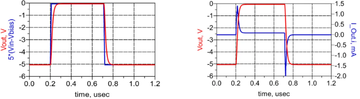
load. Left: input and output voltage pulses. Right: output voltage and current pulses. . . 40 3.9 Gate pulser PCB implementation. . . 40 3.10 Gate pulser response to 1 µs input pulses with 200 ns rise time. Left: No load,
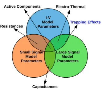
i.e., open output. Right: Loaded with a 120 pF capacitor. . . 41 3.11 Gate pulser response to 1µs input pulses with 200 ns rise time exciting a 15 W
GaN HEMT gate. Left: Output voltage. Right: Output current. . . 41 3.12 Drain pulser circuit schematic. . . 43 3.13 Drain pulser output stage circuit schematic. . . 47 3.14 Drain pulser simulation input and output voltage pulses. Left: 10Ωload resistor.
Right: 15 W GaN HEMT model biased at VGS= 0 V DC. . . 48
3.15 Drain pulser simulation output voltage and current pulses. Left: 10Ωload resis-tor. Right: 15 W GaN HEMT model biased at VGS= 0 V DC. . . 48
3.16 Drain pulser PCB implementation. . . 49 3.17 Drain pulser response to a 10µs pulse loaded with a 12Ωresistor. Left: Output
voltage. Right: Output current. . . 50 3.18 DUT test-bed. . . 51
3.19 Left: Aeroflex/INMET 8860S pulsed bias-tee. Right: pulsed bias-tee DC to RF+DC
and AC to RF+DC insertion loss, reprinted from [44]. . . 51
3.20 Current probe, TCP0030, clamped to the modified coaxial cable. . . 52
3.21 Setup diagram for pulsed I-V curves extraction using the gate pulser. . . 53
3.22 Setup diagram for pulsed I-V curves extraction using the drain pulser. . . 54
3.23 Pulsed I-V measurement setup implemented at the Telecommunications Insti-tute RF laboratory. . . 54
3.24 Close-up view of the test-bed and drain-pulser when performing measurements. 55 3.25 Example of a pulsed I-V measurement temporal diagram. . . 56
4.1 Long and short-term memory effects sources in a transistor circuit, adapted from [49]. . . 58
4.2 Dispersion in the AM-to-AM and AM-to-PM curves from a 400 W Doherty PA us-ing a wideband code-division multiple access (WCDMA) signal. Blue: Measured, Red: Modeled, reprinted from [52]. . . 59
4.3 Representative current response when voltage pulses of different time widths are applied at the gate or drain terminal of an RF FET, reprinted from [53]. . . 60
4.4 GaN HEMT simplified physical structure, reprinted from [56]. . . 61
4.5 Trapping causes representation in GaN HEMTs, reprinted from [57]. . . 62
4.6 Comparison of HEMT structures: conventional HEMT versus an HEMT with a recessed-gate surface structure, reprinted from [12]. . . 63
4.7 Knee-walkout and current collapse effect on optimum load-line for maximum output power in GaN HEMTss, reprinted from [62]. . . 64
4.8 Gate-lag process representation in a GaN HEMT, reprinted from [65]. . . 65
4.9 Exemplary voltages at gate and drain measured for the I-V curves of a 15W GaN HEMT, the values extracted correspond to the average of the samples with red circles: 13µs to 14µs. . . 66
4.10 Different sampling windows used during pulsed gate measurements in the tri-ode region. Black circles: 1µs to 2µs after the pulse rising edge. Red circles: 8µs to 9µs after the pulse rising edge. . . 66
4.11 I-V curves obtained using the different sampling windows shown in Figure 4.10, blue curves correspond to black dotted sampling window and the red curves to the red dotted window. . . 67
4.12 Gate pulsed I-V curves obtained, inside the red circle the negative slope of the curves reveal thermal effects within the 5µs and/or trapping drain related trap-ping. . . 68 4.13 Charge carrier trapping due to high drain voltages resulting in the drain-lag
ef-fect, a) and b) reprinted from [11], c) from [66]. . . 69 4.14 Pulsed VDSand the resulting IDSwith the sampling windows used marked with
red circles: 17µs to 19µs, after the voltage pulse rising edge. . . 70 4.15 Typical IDS and VDS time-domain waveforms resulting from drain-pulsed
mea-surements. . . 70 4.16 Pulsed measurement transients due to trapping of charge carriers in a 15 W GaN
HEMT. Blue trace(Step Up): VGSq = 0 V, VDSq = 0 V and VDS,peak = 30 V; Red
trace(Step Down): VGSq = −3.6 V, VDSq = 18 V and VDS,peak = 28 V, reprinted
from [67]. . . 71 4.17 Double pulsed VDSand the resulting IDSwith the sampling windows used marked
with red circles: 17µs to 19µs, after the voltage pulse rising edge. The pre-pulse was of VDS= 10 V and the gate quiescent voltage was VGSq= −3 V. . . 72
4.18 I-V curves acquired with the double pulse measurement technique for a 15 W GaN HEMT. Blue trace: VDSq,pr e= 10 V; Red trace: VGSq,pr e= 45 V. . . 72
4.19 I-V curves acquired with the double pulse measurement technique using differ-ent pre-set voltage pulses for a 15 W GaN HEMT. . . 73 4.20 Enhanced EEHEMT1 model with circuit elements describing gate and drain lag
effects, reprinted from [57]. . . 74 4.21 Schematic of the drain-lag equivalent-circuit model, reprinted from [70]. . . 75 4.22 Different I-V plots resulting from the double-pulse measurement with different
pre-set pulses of: 10 V, 20 V, 30 V and 45 V. Measured data is drawn in black, blue crosses represent the data used for the fitting of the models and the resulting fitted models are drawn in red. The resulting model parameters are forced to be the same in all the models/graphs except the threshold voltage which is al-lowed to vary for each pre-pulse voltage, i.e., each graph’s red traces represent a different model but just due to the different VT resulting from each fit. . . 76
4.23 Extracted threshold voltage versus the Vd spre-pulse voltage, reprinted from [67]. 77
A.1 Gate pulser Agilent ADS simulation schematic. The blocks corresponding to the device models used were obtained from the manufacturer. . . 89
A.2 Drain pulser Agilent ADS simulation schematic. The blocks corresponding to the device models used were obtained from the manufacturer. . . 90 B.1 Layout of the gate pulser PCB implementation on an FR-4 substrate. . . 91 B.2 Layout of the drain pulser PCB implementation on an FR-4 substrate. . . 92
1.1 Semiconductor material properties, reprinted from [9]. . . 4 2.1 Common commercial models for GaN HEMTs, adapted from [16]. . . 12 2.2 Extracted extrinsic parameters for a 3.3 W GaN HEMT. . . 18 2.3 Extracted intrinsic parameters at VDS= 15 V and VGS= −2.3 V for the 3.3 W GaN
HEMT. . . 20 3.1 Power OpAmp PB63 pin use and description. . . 44
2DEG Two-dimensional electron gas AC Alternate current
ADS Advanced Design System Al2O3 Sapphire
AM-to-AM Gain compression
AM-to-PM Phase transfer characteristic AWG Arbitrary waveform generator AlGaN Aluminium gallium nitride BJT Bipolar junction transistor CAD Computer-aided design DC Direct current
DUT Device under test
EER Envelope elimination and restoration EM Electromagnetic
ET Envelope tracking FET Field-effect transistor
GPIB General Purpose Interface Bus
GaAs Gallium arsenide GaN Gallium nitride
HEMT High electron mobility transistor HPA High power amplifier
ICCAP Integrated Circuit Characterization and Analysis Program IC Integrated circuit
IF Intermediate frequency
III-V 3rdand 5throw semiconductor elements of the periodic table IMD3 Third-order IMD
IMD Inter-modulation distortion IR Infra-red
IoT Internet of things LAN Local area network
LDMOS Laterally diffused MOSFET LED Light-emitting diode
LTME Long-term memory effects LUT Look-up table
M2M Machine-to-machine MATLAB Matrix Laboratory
MESFET Metal-semiconductor FET MET Motorola electro thermal model MIMO Multiple-input and multiple-output MMIC Monolithic microwave integrated circuit
MOSFET Metal-oxide-semiconductor FET
OFDM Orthogonal frequency-division multiplexing OpAmp Operational amplifier
PAPR Peak to average power ratio PA Power amplifier
PAE Power-added efficiency PCB Printed circuit board PC Personal computer
pHEMT Pseudomorphic HEMT
QAM Quadrature-amplitude modulation RF Radio-frequency
SMA Sub-miniature version A SNR Signal to noise ratio
SSEC Small-signal equivalent circuit Si Silicon
SiC Silicon carbide SixNx Silicon nitride
TCAD Technology CAD
TWTA Travelling-wave tube amplifier
VXI Versa Module Europa (VME) eXtensions for Instrumentation WCDMA Wideband code-division multiple access
Introduction
1.1 Wireless Telecommunications and the Power Amplifier
Telecommunications are still one of the most technology hunger fields. Despite its early times have addressed almost only military and defence applications, nowadays, both civil and military applications are big driving forces in this ever bigger market. Regarding wireless civil applications the main advantages offered by this technology are mobility, portability and ease of connection. All these advantages are possible due to the controlled emission and reception of electromagnetic (EM)-waves. The theoretical framework behind this branch of science is deeply associated with the work of Maxwell and saw first real usage when Heinrich Hertz de-veloped an oscillator. Hertz studied and created radio waves using a dipole, reason why this early type of antenna is often named the Hertz dipole.
The first transatlantic point-to-point communication link is attributed to Guglielmo Mar-coni, in 1901, and, surprisingly, it was digital! In fact, the first signals transmitted were tele-graph signals, which are more of a digital rather than analogue nature. Nevertheless, telecom-munications were already used before Maxwell, Hertz and Marconi. Going back in time, wired electrical telegraphy was already a mature and well-deployed technology by the time of the first production of EM waves. Even before electrical wired telegraphy, smoke signals, optical beams or reflected light were already used as means of communication at long distances in the 1700’s and 1800’s.
Commercial wireless telecommunications are today a huge market of billions of e’s. It started to grow significantly on the 1980’s with the development of the cell phone. On the 1990’s, the use of wireless telecommunications for personal usage lead to an exponential growth with two big areas spawning, cellular telecommunications and wireless data networks.
Cellular telecommunications are grouped in generations: 1G, 2G, and so on. The first genera-tion transigenera-tions occurred due to technological breakthroughs or big changes in the employed paradigm. Nowadays, however, the birth of new generations is more often related to market and economical reasons rather than to big technological breakthroughs. Figure 1.1 shows a comparison of the already established 4 generations of cellular telecommunications plus the forthcoming 5thgeneration, as well as a comparison between the wireless and cellular access speeds evolution over time.
AMP Analog Voice 1G 1980s 1990-1997 2000s 2020 GSM CDMA Digital Secure Voice Increased Capacity 2.5G 1998-2002 GPRS EDGE CDMA Basic Data 10- 150 Kbps 2G UMTS HSPA TD-SCDMA WCDMA CDMA2000 Enhanced Data and Capacity 1- 10 Mbps 3G LTE/ LTE-A 802.16m Broadband Data and video 100 Mbps 2010s 4G LTE/ LTE-A/LTE-LAA MMW Band Massive MIMO Enhanced Broadband Data and Video IOT M2M Ultra Reliable Ultra Fast 1-10 Gbps 5G
(a) Cellular telecommunications evolution by
generations.
“Moore’s Law for Wireless ”
(b) Wireles local area network (WLAN) and
cellular access speed over time.
Figure 1.1 Evolution of wireless telecommunications, reprinted from [1].
Access speeds kept increasing at a growing pace for both WLAN and cellular until the present days and are expected to keep on growing in the near future. The 5t h generation will bring some technical novelties such as the usage of millimetre-waves and Massive-multiple input and multiple output (MIMO), among others. These and other developments are ex-pected to allow for the dissemination of machine-to-machine (M2M), internet of things (IoT) and increase the speed, amount and reliability of data transmission.
Radio-frequency (RF) PAs are one of the most important parts of the wireless infrastruc-ture. Their purpose is to feed the antennas with sufficiently powerful RF signals such that these can be radiated and reach the receiver RF antenna/front-end at enough power levels. Given that the EM-waves get dispersed as they travel, at least proportionally to the square of distance, the most obvious way to overcome the channel attenuation is to radiate more power. If sufficient power is received, the data sent through these signals can be recovered. Generat-ing more power at high frequencies is not trivial though, at least without either doGenerat-ing that in a very inefficient way in terms of energy or using, unintentionally, more spectrum than the one actually needed due to non-linearities. In fact, due to the non-linearities inherent to these
devices, inter-modulation distortion (IMD) and spectral regrowth will arise, meaning that a relevant amount of power will be radiated at undesirable frequencies, being the most prob-lematic the ones adjacent to the frequency band/(s) being used. Actually, the latter problem gets more complicated as EM-spectrum regulators do not even allow the deployment of Power amplifiers (PAs) which contaminate the spectrum, not allocated to its intended applications, beyond a certain power level. The paradigm being discussed so far is usually short-termed as the well known linearity-efficiency compromise [2, 3].
RF PAs are usually sub-divided in classes according to their operation regime. Class-A PAs are the least-efficient and most linear class. There are many other classes, such as: B, C, D, E, F, as well as more involved topologies like the Chireix, Doherty, envelope tracking (ET) and enve-lope elimination and restoration (EER) [4–8]. Classes which are more energy efficient tend to be more non-linear as well. The non-linearities have a big impact on today’s wireless telecom-munication signals that include amplitude modulation together with frequency modulation, such as, orthogonal frequency division multiplexing (OFDM) and quadrature-amplitude mul-tiplexing (QAM). Moreover, the signals mentioned before typically have high peak to average power ratios (PAPRs), i. e., the input signal may be at lower power levels during most of the time but there will be high power peaks occasionally. Thus, having in mind that PAs are more efficient when they operate closer to saturation but also that they need to withstand the signal peaks without producing too much distortion, they are usually set to work at a given back-off power, augmenting even more the efficiency problem.
When designing the PAs that will be used in base stations, it is desirable to have the most accurate and reliable models of the electronic components that will be used. The more ac-curate the models used within computer-aided design (CAD) simulation software, the more accurate will be the final power amplifier (PA) implementation measured metrics when com-pared to the simulated ones. Furthermore, control circuitry and pre-distortion circuits be-come easier to design and their real implementation will be more predictable. This may ulti-mately lead to a first-pass design or, at least, fewer iterations will be necessary in order to meet the required specifications. New device technologies bring new possibilities and but also new challenges. It is therefore crucial to study and characterize these new devices and provide cir-cuit designers with the most accurate and complete models, exposing their advantages but also their faults. This is of paramount importance for the main component of solid-state PAs, the transistor.
1.2 Modern RF Power Transistor Technologies
Wireless telecommunications, are, nowadays, intimately related to transistor device de-velopments. More recently, wide band-gap technologies such as gallium nitride (GaN) high electron mobility transistor (HEMT) appeared. Given their relative infancy, these keep being developed or improved to fulfil size, weight, power and cost demands. Therefore, transistor and other semiconductor devices and their associated technologies continue to be a major area of research and development.
GaN materials started revealing as a promising solution for high power/frequency appli-cations in the early 90’s, [9]. Their main advantages are, among others, the higher saturated electron velocity and electron mobility, which allow higher frequency operation, as well as a wider band-gap allowing for higher breakdown fields, which translates in higher breakdown voltages and higher output powers. Table 1.1 shows a comparison of the principal properties of semiconductor technologies typically used in RF power transistors.
Semiconductor
(Typical Materials) Silicon ArsenideGallium PhosphideIndium CarbideSilicon GalliumNitride
Characteristic Bandgap
Electron Mobility at 300 °K Saturated Electron Velocity Critical Breakdown Field Thermal Conductivity Relative Dielectric Constant
Unit eV cm2/Vs #107cm/s MV/cm W/cm °K εr 1.1 1,500 1 0.3 1.5 11.8 1.42 8,500 1.3 0.4 0.5 12.8 1.35 5,400 1 0.5 0.7 12.5 3.25 700 2 3 4.5 10 3.49 1,000–2,000 2.5 3.3 >1.5 9
Table 1.1 Semiconductor material properties, reprinted from [9].
From the semiconductor physical characteristics presented in Table 1.1, it is clear that GaN has great advantages when compared to other technologies. However, due to their ma-turity, good performance and lower costs, silicon (Si) bipolar junction transistor (BJT) and laterally-diffused metal-oxide semiconductor (LDMOS) are major competitors of GaN HEMTs in the aerospace and defence markets and, the latter, in commercial base-stations. When very high power is needed, vacuum devices, such as travelling-wave tube amplifier (TWTA), are still preferred, although GaN HEMTs are starting to take their place as this technology ma-tures and its costs become lower. The numbers in Table 1.1 can be translated to more familiar PA terms such as higher power-densities due to the increased operating voltage, consequence of the wider band-gap, and current, due to higher carrier concentration. Furthermore, higher
frequencies are possible, due to the increase in mobility and saturated velocity of electrons, especially when compared to Si LDMOS.
GaN development was greatly accelerated by the pursuit of the blue and white light-emitting diodes (LEDs). In the early 1990’s, the two-dimensional electron gas (2DEG) was observed at the aluminium gallium nitride (AlGaN) hetero-junction, [10]. The formation of that electron sheet has the advantage of replacing doping techniques used in other technologies which in-troduced impurities and consequently reduced the mobility of carriers [11]. The piezoelectric characteristics of GaN material lead to higher current densities when compared with field-effect transistors FETs using Si and gallium arsenide (GaAs), the 2DEG generated can be 10 times bigger, thus increasing the current density [12]. However, there are some less positive aspects about GaN too, the first is that there are still no GaN substrates and typically Si, sili-con carbide (SiC) or sapphire (Al2O3) are used, all of them with their advantages and
disad-vantages. Furthermore, GaN thermal conductivity does not follow the power density increase and may limit the maximum power achievable in practice. There is also a negative aspect about the piezoelectric behaviour of the device, high fields can cause structural damage due to mechanical stress which can affect the reliability of the technology.
One of the most important causes for the lack of accuracy between simulations and mea-surements of GaN based RF PAs is the trapping of charge carriers. These phenomena has drawn a considerable amount of attention from researchers and industry at both the device physics and production levels. Furthermore, it is a relevant topic in the RF modelling and PA design fields. Without getting too much into the physics and device production sides, RF en-gineers and modellers need to focus on the accurate characterization and understanding of these mechanisms so that they can be properly studied and modelled and their impact accu-rately predicted and/or mitigated.
1.3 RF Power Transistors Modelling
Modelling of RF components is a necessary step in order to fully exploit the power of cir-cuital simulators. Without proper models, the practical impact of these software tools would be much more limited. Modelling active devices, such as transistors, can be a reasonably dif-ficult task, at least within decent limits of usability, size and ease of extraction from the mea-surements one can obtain from these devices. Therefore, several modelling approaches and extraction methodologies are used, such as, behavioural and compact models.
multi-dimensional parameters such as bandwidth, efficiency, linearity and power. The be-haviour of these devices can be very different under large-signal conditions than for small-signals. Furthermore, electro-thermal effects are often a critical issue and require isothermal measurements or other temperature controlled characterization. Moreover, emerging wire-less technologies use more complex digital modulations which brings new challenges in the modelling and design processes.
A modelling abstraction level hierarchy is depicted in Figure 1.2. At the lower abstraction levels there are the physics based models, which are seeing increased use, namely in the tech-nology development iterations, in what is called techtech-nology CAD (TCAD). Then we have com-pact models, that bridge the physics of the device into equivalent circuits, amenable to be integrated in circuit simulator where Kirchhoff’s current and voltage laws are used. The phys-ical meaning of the parameters may be lost though, but the complexity and simulation time is greatly reduced. Behavioural models, lie at a fairly high level of abstraction but they are becoming more valuable as the need for digital pre-distortion increases and therefore, com-putationally efficient and fast to extract system/circuit models are required.
Figure 1.2 A general modelling design abstraction level hierarchy, reprinted from [13].
Compact models are very often used at the device level, these rely on an equivalent linear circuit topology or “template”, which is appropriately selected or developed for the technol-ogy/device to be modelled. Besides the linear elements, analytical expressions for the non-linear components such as capacitances, current-sources, diodes, etc. are used as well. To ex-tract these parameters, more than one measurement type is recommended. Figure 1.3 shows which measurements are typically used to extract the different compact model parameter
types from. The overlapping of different type of measurements used to extract the same pa-rameters can be observed, which means that different measurements can be used to extract the same parameters and validate each other. The non-linear active components such as the current source, need to be consistent in all of the measurements space. However, electro-thermal and trapping effects are only observable and thus extractable when the device is driven with sufficiently powerful signals such that the device temperature or trapping state changes. Recent trends in device modelling for circuit design, including PA design, tend to use compact models together with electromagnetic simulations, due to the ever increasing shift upwards in the frequency spectrum.
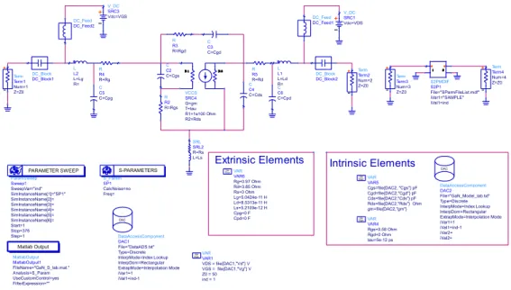
Transistor Model Parameters
I-V Model Parameters Active Components Large Signal Model Parameters Small Signal Model Parameters Resistances Electro-Thermal Trapping Effects Capacitances
Figure 1.3 Measurements from which the non-linear transistor compact model parameters are
extracted.
1.4 Pulsed DC I-V and Trapping Related LTME
The actual RF operating conditions are often not attainable at the measurement environ-ment, either due to current/voltage/power constraints or the limitation in pulse widths of pulsed measurements. Nevertheless, several types of measurements can, or need to, be used in order to obtain an accurate model of an RF power transistor. Direct current DC measure-ments are important to model the device’s current-source voltage dependence but they may heat-up the device and ultimately destroy it. Therefore, I-V graphs are typically drawn from
pulsed measurements, called pulsed DC I-V. The used pulses are too long to be considered in the RF range, and that is why they are called DC, even though they are obtained from pulsed excitations. Moreover, these type of pulsed excitation may be used to bias the device and thus allow the measurement of bias-depend pulsed S-parameters which are desirable at any FET or HEMT compact modelling process.
Although very important for the characterization of transistor devices, pulsed measure-ments can be very useful as well in the observation and characterization of long-term memory effects (LTME) related to either temperature, bias-networks or electron trapping. The figures of merit of GaN HEMT based PAs resulting from computer simulations are often too far from what is measured of their real implementation. One of the reasons for that is the limited mod-elling of LTME which prevents the prediction of the negative impact these effects have on the overall circuit implementation. Thus, in this work, pulsed measurements were aimed at the characterization of LTMEs, particularly caused by the trapping phenomena.
Figure 1.4 shows a general pulsed excitation waveform and the sampling windows and durations one may choose. To obtain isothermal I-V curves it is important to use, not only a low duty cycle but also a narrow pulse. However, if it is too narrow the sampling window falls into the transient response and the resulting measurements become less reliable.
Time
Meas
urement
V
al
ue
Wait time for DC Measurement
Wait time for Fast IV Measurement
Transient Response
Long Averaging (DC)
Minimum Averaging
Figure 1.4 Pulsed I-V measurement waveform shape and sampling time window representation.
The trapping of charge carriers is known to affect III-V devices, namely high power GaN HEMTs. This occurs at time-scales which are below the high-frequency charge storing phe-nomena, ns, and above thermal effects, ms. Therefore, with a high peak power pulsed I-V measurement system, able to provide voltage and current pulses or other pulse-shaped wave-forms at theµs scale, these phenomena can be observed, and characterized.
1.5 Dissertation Objectives
The purpose of the work here reported was to develop and implement a pulsed I-V mea-surement setup in order to observe and characterize LTME caused by the trapping of charge carriers in RF power GaN HEMTs. To accomplish that goal, and given that dedicated pulsed measurements hardware are extremely costly and their flexibility is somewhat limited, an “in-house” measurement setup was developed, relying on two electronic circuits that were designed and implemented, called throughout this document as pulsers. The setup was con-trolled through MATLAB scripts such that pulsed I-V curves could be obtained with some flexibility in the pulse widths, periods and shapes used. Through properly designed pulsed excitations, LTME could be observed in the measured I-V curves and their time constants ex-tracted.
1.6 Dissertation Outline
This document is organized as follows.
Chapter 2 overviews the most common RF power transistors modelling techniques, with emphasis on compact models. Additionally, the extraction of a bias-dependent small-signal equivalent circuit from pulsed S-parameters is described.
Chapter 3 presents the development of a pulsed I-V measurement setup, including the design of the drain and gate pulsers, as well as the measurement setup block architecture and control methods.
Chapter 4 addresses LTME, in particular those related to charge carriers trapping phe-nomena and how pulsed DC I-V measurements can be used to characterize and model these effects.
RF Power Transistors Modelling
During circuit and system design process, CAD software is an essential tool, in both indus-try and research. It is, therefore, fundamental to provide RF circuit designers with accurate and reliable models that can help reducing time and production costs. These better models may, ultimately, lead to first-pass designs instead of the time-consuming iterative design pro-cesses. Transistor models should be easily extractable and to include in commercial simulator software. Convergence and simulation speed are also important features researchers and de-signers usually take into account.
There are mainly three types of modelling approaches: physics based, compact and be-havioural modelling. Models based on the physical structure of the device are fundamental when developing new materials and technologies. They can be very insightful and cover wide device operating ranges but the complexity in their extraction and the processing time re-quired to solve the associated complex difference equations in simulators, such as Poisson’s and the electron and hole continuity equations are major drawbacks, even in a powerful com-puter. Furthermore, they are less flexible, since a new device structure or material may require a very different model.
Compact models, are half-way between the physics approach and a completely empirical one. They still rely on the nature of the device but reduce much of the physics computation complexity making use of equivalent circuit elements and a set of parameters which are in-tended to be easily extractable.
Behavioural, black-box or measurement based, models map the input output relation-ships with none or very few previous knowledge about the device or system to be modelled. These are more often used at a higher level of abstraction in overall circuit and system de-sign [13].
Compact models may also be divided into physics-based or measurements based. The former make use of the physical properties of the device such as its structure dimensions and doping level [14], whereas in the latter, semi-empirical parameters or a set of look-up table (LUT) are extracted from device measurements, both containing one or more linear or non-linear equivalent circuits. The behavioural model approach resembles the measurement based compact model despite being defined separately, due to the more mathematical and systematic nature. Figure 2.1 shows a general comparison between different modelling ap-proaches. Compact model Behavioural model Physic model Physical insight Operating range Convergence Extrapolation Accuracy Easy modeling
process Usability for Circuit design
Figure 2.1 Qualitative comparison between different RF PA modelling approaches, adapted
from [15].
Compact models are very often used by circuit designers and regarded as the industry standard. This modelling approach will be the one used in this work. Table 2.1 contains some FET and HEMT commercial available models.
FET Model Number of
Parameters Thermal Effects Trapping Effects Original Device Context
Curtice3 59 No No GaAs FET
CFET 53 Yes No HEMT
EHMET1 71 No No HEMT
Angelov 80 Yes No HEMT/MESFET
AMCAD HMET1 65 Yes No GaN HEMT
The compact model parameter extraction is a fairly difficult and time-consuming process. A generic model extraction flow, Table 1.1, involves different measurement procedures. The two most important are pulsed I-V and pulsed S-parameters. With these measurements the core device model can be created as a LUT, indexed by the terminal voltages, vGS and vDS.
This can thus be regarded as a non-linear model made of a set of liner-models although care should be taken on how the data is interpolated between sets. The LUT approach may result in large amounts of data and usually a suitable non-linear analytic model, whose parameters can be fitted to the measurement data, is used. This model is then called a non-linear compact model as it is much lighter than the LUT approach, given that only a set of parameters need to be stored. The current-source and some capacitances are typically modelled as non-linear while other equivalent circuit elements are standard linear components commonly used in simulators.
Parameter2extraction2methodology
Pulsed IV / S parameter measurement results Specific measurements Power measurements Multibias set of linear modelsNonlinear model Enhanced
Nonlinear model Final Nonlinear model 1ststep: bias-dependant2S parameters - diodes - g-d2breakdown - thermal2effects - charge2carrier2trapping -load-pull2measurements CW,2pulsed 2-tones time2domain 3rdstep: setting2of additional parameters 4thstep: implementation2in commercial2simulator 5thstep: validation2and refinement Core2device2model 2ndstep: large signal2fitting Model2Enhancement Model2Validation
Figure 2.2 Modelling procedure flowchart, reprinted from [17].
After the core model is extracted, extra features can be added to it. Less important charac-teristics such as parasitic junction diodes and breakdown may also be added. Thermal effects and charge carrier trapping are, however, very important features that can change dramati-cally the device model behaviour affecting its operation in a PA circuit. Therefore, modelling both trapping and temperature effects is of paramount importance for accurate simulation results.
When the complete model is extracted, many types of validation and performance mea-surements can be taken and their results used for further refinement of the model. Usually, PA designers want to achieve the highest possible efficiency and output power while keep-ing sufficiently high linearity. That is why most models are designed and extracted to predict, as accurately as possible, the figures of merit related with these requirements, such as IMD, power-added efficiency (PAE), etc.
During the development of the transistor model, we should bear in mind the following Laws of Simulation and Modelling [13]:
(i) A simulation is only as accurate as the models it is based on; (ii) A model is (mostly) useless unless it is embedded in a simulator; (iii) Models are, by definition, inaccurate; it’s just a matter of degree; (iv) Models generally trade off complexity (simulation time) for accuracy.
2.1 DC Modelling: I-V Curves
The DC behaviour of a FET, or other types of transistors, is usually expressed trough an I-V plot. This type of representation is very compact since just one graph may contain much information about the behaviour of the transistor. I-V graphs drawn from the same transistor can change dramatically according to their measurement conditions. That said, it is very im-portant to mention under which measurement conditions the data used in these graphs was obtained. The x-axis represents VDSand the y-axis IDS. Usually, several curves are drawn, one
for each gate voltage, VGS.
Figure 2.3 shows a typical IDS-VDS plot of a FET. Several effects are emphasized on the
curves, particularly the drain current decrease due to thermal effects. This characteristic ap-pears when the I-V curves are based on DC measurements and the power dissipated at device, i.e., the IDS× VDSproduct, is sufficiently high to induce self-heating and cause a current
de-crease. Note that, if the curves in Figure 2.3 represented the actual dynamic behaviour under RF operation of the transistor, a strange phenomena would appear to happen, given that the negative slope of the curves measured at higher Vd swould mean a negative drain resistance,
Rd s, or conductance, gd s.
DC I-V measurements are simple, fast and widely used, mostly for small gate-periphery devices, i.e., low power devices requiring small amounts of current. This type of measure-ments is extremely important since the main non-linearities of a FET come from its voltage-current relationship and so these constitute an important starting point for the large-signal
model [13]. To be able to produce I-V plots which are not temperature dependent, pulsed I-V measurements were introduced. This type of characterization is one of the topics of this work and will be addressed in Chapter 4.
reverse operation
knee region self-heating
breakdown Id (mA) Vds(V) −5 0 5 10 15 20 25 30 0 60 40 −20 −40 −60 −80 20 80 100
Figure 2.3 Typical DC I-V curves of a FET highlighting different typical characteristics of these
devices, reprinted from [18].
2.2 Small-Signal Equivalent Circuit: SSEC
S-parameters are the most used measurements in order to capture the RF behaviour of a device under test (DUT). Being a linear representation of the high frequency behaviour of the device, they accurately represent its operation in the small signal regime at the operating bias point, VDSq and IDSq, under which they were measured. Therefore, a set of S-parameters must
be taken for each different bias so that one can get the device RF behaviour at all the regions of interest.
Having in mind the way S-parameters measurements are taken for each bias condition of a FET, one can better understand the meaning of the small-signal equivalent circuit (SSEC). That is also one of the reasons for the compact model naming, since the physical phenom-ena of a rather complex device is mapped through an equivalent circuit. Although most of the extracted elements are indeed well described as linear, some of them are converted to non-linear, either through the use of properly fitted mathematical functions or by using LUTs
indexed by the terminal voltages at the device. The former can model accurately the extracted parameters and be continuous and differentiable up to a given order, depending on the qual-ity of the mathematical functions used. The latter are a direct result of the circuit parameters extracted from the S-parameter data which need to be interpolated or processed in order to cover the device’s full operating range and be useful for non-linear simulations.
To obtain the SSEC model a sequential procedure is used to extract the circuit elements. As pointed in [16], one of the SSEC advantages is that it links the physical structure of the device to its circuit behaviour allowing the connection between the RF performance and the geometry of the device. It is also important to notice that models and their associated ex-traction procedure, which are known to work well for a matured technology such as GaAs metal-semiconductor FET (MESFETs) may provide less reliable results for less mature ones, such as, GaN HEMTs. In any case, the results of applying the modelling techniques already used for GaAs MESFETs on GaN HEMTs appears to result in fairly good models, since most key features are common to both technologies and the SSEC is a general representation that is relatively flexible.
There are, in literature, many works on small-signal modelling approaches. Three of the more widely known are the ones by Dambrine et al. [19], Berroth and Bosch [20] and Rorsman et al. [21]. A SSEC topology for a general FET is presented in Figure 2.4. From it, one can dis-tinguish two types of elements: extrinsic and intrinsic. The structure that surrounds the die, which includes or may include the bond-wires, pre-matching capacitors, the substrate, access pads and the device’s package is represented by the extrinsic or parasitic elements, which are, in Figure 2.4, outside the shaded rectangle. Extrinsic elements are considered to be frequency and bias independent. On the other hand, the transistor die is represented by the intrinsic elements which are still modelled as frequency independent but now as bias dependent and are, thus, extracted for each bias point.
The SSEC adopted here, especially the extrinsic part, is a fairly simplified and general one, whose structure is more suitable for smaller devices. When modelling devices of larger gate periphery and/or an higher accuracy is desired, effects like inter-bond-wire capacitances and mutual inductances as well as substrate leakage, can be added to the SSEC. Hence, more ex-trinsic equivalent circuit elements are needed, which can even be of distributed nature, e.g., transmission lines.
To determine the extrinsic parameters one can choose between two approaches [16]: us-ing dummy structures, i.e., removus-ing the active part of the device and perform measurements with just the remaining passive structure, or applying the ’cold-FET’ technique, i.e.
measur-ing S-parameters at VDS= 0 V for two different gate conditions: strong forward bias and below pinch-off. Cgd Rs Ls Cpd Port2 Ld Rd Port1 Rg Cpg Lg Rds Cds gm Rgs Cgs -jωτ e
Figure 2.4 Small signal equivalent circuit topology, SSEC, adapted from [18].
The aim of the ’cold-FET’ technique is to put the transistor under two different conditions at which the effect of the extrinsic structure will become minimally affected by the active die and, thus, easier to extract. Figure 2.5 shows the inside of two different HEMT packages re-vealing some of the extrinsic structures previously mentioned.
(a) M et al-ceramic package (b) Plast ic packages
Figure 2.5 RF power transistor plastic and ceramic packaging examples, reprinted from [13].
After determining the extrinsic elements one can proceed to the de-embedding of the intrin-sic S-parameter by removing the effect of each extrinintrin-sic element from the global S-parameter data. This is done by changing appropriately from S to Z or Y parameters while removing the contribution of this elements from the global S-parameters, as reported in [19]. It is important to refer that errors in the extrinsic parameter extraction and de-embedding will most proba-bly affect the following steps. This will make the model less accurate, either due to the choice of an inadequate model topology, a poor extraction method or even both.
The parasitic inductances are extracted first from the high frequency imaginary part of the Z parameters when the device is biased with VDS = 0 V and VGS = 2 V. The extracted
induc-tances are then de-embedded from the from the Z-parameters for VDS= 0 V and VGS= −4 V
and these are converted to Y-parameters to find the capacitances. However, the direct appli-cation of the method in [19] resulted in negative values for the intrinsic capacitances. There-fore these were set to 0. The extrinsic resistances were determined according to [19] assuming that Rs ≈ 0Ω. This provided physically consistent results, i.e., the resulting S11 and S22
af-ter de-embedding, stayed inside of the Smith Chart. The parameaf-ters extracted from pulsed S-parameter measurements (obtained through an Auriga system) of a 3.3 W, 1 mm gate pe-riphery GaN HEMT from SEDI, Inc. biased at Vd s,q = 50 V and Vg s,q = −5 V are shown in
Table 2.2. Despite having set to 0 the parameters that could not be extracted, all the remain-ing ones provided a reasonably good startremain-ing point suitable for further refinement through optimization in a CAD software tool after a first guess for the complete model, including the intrinsics, is determined. Parameter Value Ld 85.4 pH Lg 50.4 pH Ls 5.2 pH Rd 3.85Ω Rg 0.97Ω Rs 0Ω Cpd 0 pF Cpg 0 pF
Table 2.2 Extracted extrinsic parameters for a 3.3 W GaN HEMT.
The intrinsic part of the SSEC, inside the rectangle in Figure 3.4, is often represented us-ing Y parameters. These are better suited to describe theπ-topology of the SSEC and result in simpler expressions for estimating the element values at low frequencies. Without the extrin-sic elements, the SSEC can be expressed as follows,
Yi nt= " Y11 Y12 Y21 Y22 # = Yg s+ Yg d −Yg d −Yg d+ gme− j ωτ 1 + j ωRg sCg s Yd s+ Yg d , (2.1) with,
Yg s= 1 jωCg s + Rg s , (2.2) Yd s= 1 Rd s+ j ωCd s , (2.3) Yg d= j ωCg d, (2.4)
and each parameter can be estimated through the following relations,
Cg d= − 1 ωI m{Y12}, (2.5) Cd s= 1 ωI m{Y12+ Y22}, (2.6) Rd s= Re{Y12+ Y22}−1, (2.7) Cg s= 1 ωI m{Y11+ Y12}, (2.8) Rg s= 1 ω2C2 g d Re{Y11+ Y12}, (2.9) gm= |Y21− Y12|, (2.10) τ = − 1 ωphase{Y21− Y12}. (2.11)
Note that in order to separate real and imaginary parts of the Y parameters, a denominator of the type:
D = 1 + ω2R2C2, (2.12)
appears, and the Equations (2.5) and (2.11) rely on approximations of the same kind as,
D = 1 + ω2R2C2≈ 1, (2.13)
which can be made with minimal effect on the final result if the parameters are extracted at low enough frequencies. There is no Rg d in series with Cg d in Figure 2.4 due to the difficulty
in finding a resistive component consistently in S12 and S21. Despite that shortcoming, the
impact of that element in the circuit behaviour is hardly noticed and some published SSECs do not even consider this element. From Equations (2.5) and (2.11), the intrinsic elements were determined for each bias point, through a linear fit at lower frequencies. The parameter values obtained for VDS= 15 V and VGS= −2.3 V are shown in Table 2.3.
The procedure described before is a generalized one since the extrinsic structure of RF power transistors can be much more complex and also because the method applied was de-veloped for the more mature GaAs MESFET technology. Thus, although it works reasonably well, care should be taken when applying it to GaN HEMTs, especially for the extrinsic
param-eter extraction. In [18], for example, it is referred that the equivalent circuit which represents the transistor in the ’cold-FET’ condition will not be easily extractable under strong forward-bias, since the conduction band of GaN HEMTs is much higher than that of GaAs devices.
Parameter Value Cg s 1.96 pF Cg d 81.93 fF Cd s 0.26 pF Rg s 0.58Ω Rg d 0Ω Rd s 590Ω gm 125 mS τ 5.13 ps
Table 2.3 Extracted intrinsic parameters at VDS= 15 V and VGS= −2.3 V for the 3.3 W GaN HEMT.
Some of the parameters obtained are depicted in Figure 2.6 versus frequency. The capaci-tances, gmandτ remain relatively constant up to 10 GHz and Rg sfrom 2 GHz to 10 GHz.
0 2 4 6 8 10 12 14 16 18 20 22 0 0.5 1 1.5 2 2.5 3 3.5 4 4.5 5 5.5 6 6.5 Frequency (GHz) Cgd ,Cds ,C gs (pF), τ (ps) Rgs ( Ω ) , g m (S) C gd C ds C gs τ R gs 10xg m
Figure 2.6 Intrinsic parameters versus frequency obtained at VDS= 15V and VGS= −2.3 V for a
3.3 W GaN HEMT.
This indicates that one has to carefully select which zones to use for the fitting and verify the validity of that choice. It may also be related with the measurement noise which, indirectly im-pacts the extraction and the parameter equations themselves, as these, are lower frequency approximations taken from an equivalent circuit, itself already an approximation. Neverthe-less, the results can be very accurate, actually as accurate as the complexity of the model and the measurements used to build it allow.
2.3 Extending the Model to Large-Signal
The SSEC determined previously is the result of a set of small-signal S-parameter mea-surements. However, RF power transistors are typically operated under large signals in such a way that the highest possible output power can be drawn from the device with the high-est possible efficiency and linearity. Therefore, effects like temperature, junction diodes’ be-haviour and breakdown should be added to the model. Furthermore, under actual telecom-munication signals other important effects, such as long-term memory effects, may degrade the expected performance and, thus, need to be taken into account in a complete model. The capability of the extracted set of small-signal models in predicting distortion in a simulator is limited by the discrete nature of the measurements, i.e., finite amount of data points. Ad-ditionally, part of the extracted SSEC parameters are bias-dependent and may result in large amounts of data that need to be stored, which is less suitable to be used in a compact model.
2.3.1 Multi-Bias Linear Models
Although not suitable to include in commercial models, the bias-dependent SSEC data set may be used to validate the extracted model by comparing it with the device S-parameter measurement data. To do so, a model that accesses a LUT was created in Agilent Advanced Design System (ADS), Figure 2.7.
Extrinsic Elements Intrinsic Elements
Var Eqn
Var Eqn
S-PARAMETERS
PARAMETER SWEEP EqnVar
DAC Matlab Output Var Eqn DAC L R R L S2PMDIF Term C DC_Feed DC_Feed DC_Block DC_Block C DataAccessComponent MatlabOutput Term C C SRL Term Term VCCS ParamSweep VAR VAR VAR V_DC V_DC S_Param VAR R C R DataAccessComponent L2 R4 R5 L1 S2P1 Term4 C5 DC_Feed2 DC_Feed1 SRC4 DC_Block2 DC_Block1 C3 C2 MatlabOutput1 SRL2 Term3 C4 C6 Term1 Term2 Sweep1 VAR5 VAR4 DAC1 VAR6 SRC1 SRC3 SP1 VAR1 R2 R3 DAC2 R= L=Lg R= L=Ld R=Rd R=Rg iVal1=ind iVar1="SAMPLE" File="SParmFileList.mdf" Z=Z0 Num=4 tau=5e-12 ps C=Cgs L=Ls iVal2= iVar2= iVal1=ind-1 iVar1=1 ExtrapMode=Interpolation Mode iVal1=ind-1 R2=Rds C=Cgd R1=1e100 Ohm iVar1=1 FilterExpression="" UseCustomControl=yes Analysis=S_Param FileName="GaN_S_lab.mat." R=Rs G=gm C=Cds Num=3 C=Cpg Z=Z0 Num=1 Z=Z0 Num=2 C=Cpd Step=1 Stop=376 Start=1 SimInstanceName[6]= SimInstanceName[5]= SimInstanceName[4]= SimInstanceName[3]= SimInstanceName[2]= SimInstanceName[1]="SP1" SweepVar="ind" Cgs=file{DAC2, "Cgs"} pF Cgd=file{DAC2,"Cgd"} pF Cds=file{DAC2,"Cds"} pF Rds=file{DAC2,"Rds"} Ohm gm=file{DAC2,"gm"} Rgs=0.58 Ohm Rgd=0 Ohm File="DataADS.txt" Type=Discrete InterpMode=Index Lookup InterpDom=Rectangular ExtrapMode=Interpolation Mode Z0 = 50 Rg=0.97 Ohm Rd=3.85 Ohm Rs=0 Ohm Lg=5.0424e-11 H Vdc=VDS Vdc=VGS Ld=8.5313e-11 H Ls=5.2109e-12 H Cpg=0 F Cpd=0 F Z=Z0 Freq= CalcNoise=no T=tau VGS = file{DAC1,"Vg"} V VDS = file{DAC1,"Vd"} V ind = 1 R=Rgs R=Rgd File="GaN_Model_lab.txt" Type=Discrete InterpMode=Index Lookup InterpDom=Rectangular
Figure 2.7 SSEC ADS schematic used for comparison with S-parameter measurement data of a
The bias-dependent small signal elements were imported from a previously generated file in MATLAB making the overall model consisting of many linear models. The model simula-tion S-parameter data was exported to MATLAB for comparison with the measured device S-parameters that were initially used to extract the SSEC model.
Figure 2.8 shows the comparison between the measured S-parameter and the simulation of the developed model for two different bias conditions.
0.2 0.4 0.6 0.8 1 30 210 60 240 90 270 120 300 150 330 180 0 Measurements Simulation 25xS 12 S 11 S 22 S 21/20 (a) VDS= 30 V and VGS= −2.3 V. 0.2 0.4 0.6 0.8 1 30 210 60 240 90 270 120 300 150 330 180 0 Measurements Simulation 2xS12 −2xS 21 S11 S22 (b) VDS= 0 V and VGS= −2.3 V.
Figure 2.8 Comparison between model and measurements from 500 MHz to 10 GHz.
0.2 0.5 1.0 2.0 5.0 +j0.2 −j0.2 +j0.5 −j0.5 +j1.0 −j1.0 +j2.0 −j2.0 +j5.0 −j5.0 0.0 ∞ Measurements Simulation S11 S22 −S 22 S11 Cut−off Forward Bias
Figure 2.9 Comparison between model and measurements from 500 MHz to 10 GHz under the
’cold-FET’ condition (VDS= 0 V), at VGS= −4 V (cut-off) and VGS= 2 V (forward bias).
used such that S12 and S21could be drawn on the same chart. The Smith chart depicted in
Figure 2.9 shows the comparison between measured and modelled S-parameters, S11and S22,
with the device in the ’cold-FET’ condition.
The extrinsic elements were extracted from measurements under the conditions previ-ously mentioned. An inductive behaviour can be observed for strong-forward bias whereas the capacitive nature of the device for the below pinch-off biasing becomes clearly visible. The results from the model simulation are in good agreement with the measurements in this condition too. Note that the cut-off S22in Figure 2.9 is rotated 180◦for better visualization.
2.3.2 Non-linear Models
To improve the model compactness and avoid the shortcomings in terms of resolution and lack of continuous differentiability of the LUTs approach, models usually consist of non-linear analytical functions that were fitted to the device’s measurement data along VGS, VDS
or both. These non-linear functions contain parameters that may be firstly set from visual in-spection of the DC I-V characteristics or its partial derivatives, gmand gd s, extracted from
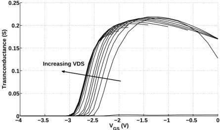
S-parameters of the device and later optimized in a software tool. Depending on the number of parameters and the choice of suitable analytical functions, very accurate and compact mod-els can be developed. Figures 2.10 and 2.11 show two of the non-linear elements extracted from the de-embedded S-parameters, gm and Cg s, which can be fitted to properly selected
non-linear functions. It is most noticeable that both parameters are strongly VGS dependent,
although some variation with VDSis also visible.
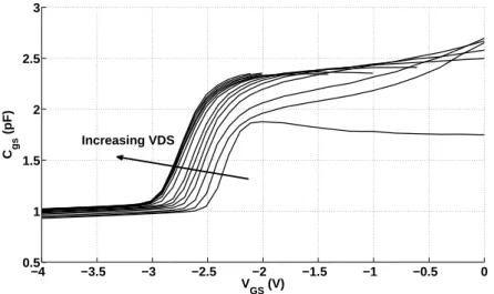
−4 −3.5 −3 −2.5 −2 −1.5 −1 −0.5 0 0.5 1 1.5 2 2.5 3 VGS (V) C gs (pF) Increasing VDS
After verifying that the extracted parameters are reasonably accurate, one can evaluate how each of the parameters expected to be non-linear varies with gate and drain voltages. If the parameter or equivalent circuit element is strongly dependent on just one input voltage,
vDSor vGS, a two-dimensional fitting, inR2, may be discarded. This will reduce the complexity
and avoid non-physical results like violations of the charge conservation principle which may appear when non-linear capacitances are not exclusively dependent on their terminal volt-ages. Furthermore, the used non-linear mathematical functions are time independent which is referred in literature as the quasi-static approximation [22].
−40 −3.5 −3 −2.5 −2 −1.5 −1 −0.5 0 0.05 0.1 0.15 0.2 0.25 VGS (V) Trasnconductance (S) Increasing VDS
Figure 2.11 Extracted SSEC gmversus VGSfor VDS= 0 V to VDS= 100 V.
The author of [23] describes a non-linear current source model used for a GaN HEMT. That model will be the used in Chapter 4, with the addition of a charge carrier trapping related LTME part, obtained from pulsed DC I-V measurements. Similarly to other models proposed in literature, it can be generally expressed as,
iDS(vGS, vDS) = β · fg(vGS, vDS) · fd(vGS, vDS), (2.14)
where the output current iDS is defined as the product of two functions, fg(.) and fd(.), and a
scaling factor,β. Although both drain and gate voltages are input parameters for both func-tions they are separated and written with different subscripts to represent their stronger rela-tionship with each control voltage. The device threshold voltage is taken into account through the linear function,
![Figure 2.1 Qualitative comparison between different RF PA modelling approaches, adapted from [15].](https://thumb-eu.123doks.com/thumbv2/123dok_br/15912268.1092821/38.892.177.718.420.672/figure-qualitative-comparison-different-rf-modelling-approaches-adapted.webp)
![Figure 2.3 Typical DC I-V curves of a FET highlighting different typical characteristics of these devices, reprinted from [18].](https://thumb-eu.123doks.com/thumbv2/123dok_br/15912268.1092821/41.892.231.669.274.601/figure-typical-highlighting-different-typical-characteristics-devices-reprinted.webp)
![Figure 3.2 Specifications for several pulser heads available from Auriga Microwave, reprinted from [32].](https://thumb-eu.123doks.com/thumbv2/123dok_br/15912268.1092821/59.892.161.749.342.572/figure-specifications-pulser-heads-available-auriga-microwave-reprinted.webp)
![Figure 3.4 Pulsed I-V instrument architecture diagram, reprinted from [38].](https://thumb-eu.123doks.com/thumbv2/123dok_br/15912268.1092821/61.892.257.647.319.605/figure-pulsed-i-v-instrument-architecture-diagram-reprinted.webp)