Miguel Simão Farto
Licenciado em Ciências de Engenharia de Micro e Nanotecnologias
M
ULTIPURPOSE
XRD
HOLDER FOR THE
SIMULTANEOUSLY CHARACTERIZATION OF THE
S
TRUCTURAL AND
E
LECTRICAL PROPERTIES OF
VANADIUM OXIDES
Dissertação para obtenção do Grau de Mestre em Engenharia
de Micro e Nanotecnologias
Orientador:
Doutora Joana Maria Dória Vaz Pinto Morais Sarmento,
Professora Auxiliar Convidada, Faculdade de Ciências e
Tecnologias da Universidade Nova de Lisboa
Co-orientador:
Doutor Rui Alberto Garção Barreira do Nascimento Igreja,
Professor Auxiliar, Faculdade de Ciências e Tecnologia da
Universidade Nova de Lisboa
Julho 2019 Júri:
Presidente: Professor Doutor Rodrigo Martins Arguente: Doutor Jonas Deuermeier
iii
Multipurpose XRD holder for the simultaneously characterization of the Structural and Electrical properties of vanadium oxides
Copyright © Miguel Simão Farto, 2019.
A Faculdade de Ciências e Tecnologia e a Universidade Nova de Lisboa tem o direito, perpétuo e sem limites geográficos, de arquivar e publicar esta dissertação através de exemplares impressos reproduzidos em papel ou de forma digital, ou por qualquer outro meio conhecido ou que venha a ser inventado, e de a divulgar através de repositórios científicos e de admitir a sua cópia e distribuição com objetivos educacionais ou de investigação, não comerciais, desde que seja dado crédito ao autor e editor.
v
“Life is like a box of chocolates. You never know what you're gonna get.” Forest Gump
vii
Acknowledgements
Gostaria de começar por agradecer a todos os que me ajudaram a ultrapassar esta etapa da minha vida. Muito, mas mesmo muito obrigado!!
Queria inicialmente agradecer à Faculdade de Ciência e Tecnologia e ao Departamento de Ciências dos Materiais por terem sido uma nova casa para mim, que levo no meu coração para o resto da vida! Em especial gostava de agradecer ao professor Rodrigo Martins e à professora Elvira Fortunado pelo seu empenho e ambição em criar um curso inovador no nosso país e pelas magnificas condições por vocês criadas no CENIMAT e no CEMOP.
À minha orientadora professora Joana Vaz Pinto e co-orientador professor Rui Igreja pelo fantástico apoio nesta minha jornada, um muito obrigado!
Ao pessoal do Open Space, CENIMAT e CEMOP, por todo o apoio, amizade e boa disposição ao longo deste tempo, a ti Cátia, Inês, Marco, Andreia, Rodrigo, Sara, Bea, Paul, Inês, Ribas e Farinha, obrigado! Não me poderei esquecer do primeiro grupo de sempre do novo espaço, o Close Space, Bela, Xana, Chico e Vasco, acho que ficamos na história. E aos amigos que também levo da faculdade, Manu (que tanto que aturou e ajudou), Diogo, Bruno e André, acho que finalmente acabamos todos!
À minha família do continente, que tanto foram importantes para acolher o “rapaz das ilhas”, um muito obrigado tia Naide, Gonçalo, Maria, tia Laidinha, tio Ilídio, Ricardo, tia Paula, tia Cantante, André, Teresa e claro à matriarca da família avó Casimira. Ao João, à Sérgia, ao Diogo, à Sofia, ao João, ao Tó Manel e à D. Etelvina que foram como uma segunda família. Aos meus compadres Adriana e Luis, ao seu rebento, meu afilhado Dinis!
Às meninas do Barreiro, Ana Cláudia, Ana Sofia, Gabi e Nádia, às minhas meninas de Conservação e Restauro, Daniela, Joana, Rita e Rosa, apesar de não estarmos sempre juntos a amizade fica para sempre! Obrigado!
Atravessando agora meio oceano, à minha família dos Açores, à minha tia Armanda, tio Luis, tio Manecas, tia Zélia, tio Pedro, Hugo e Rodrigo, um muito obrigado! Aos meus padrinhos Zé e Rosa e às filhas Júlia e Rita por todo o apoio.
Ao pessoal do karaté, sensei João Guiod de Castro, Ritta, Maria Inês e Mota. Aos amigos que resultaram do Folk Azores, Ana Rita, Andreia, Carolina, Cat, Rita e Jason!
A ti Stefanie, que sempre me aturaste nas melhores alturas, nas piores alturas, nos momentos mais sérios, nos momentos mais parvos (que são demasiados eu sei), danke!
À família de casa, ao meu irmão Luis, Filipa, Nídia e Lúcia (que apesar de já não cá estares, ficas sempre cá). Por último e não menos importante, aos meus pais, pai Rui e mãe Lúcia pelo apoio incondicional desde que me puseram ao mundo, pela vida que me proporcionaram e continuam a proporcionar! Um muito obrigado!
ix
Abstract
Several oxides present a severe and reversible resistance changes with the application of an external stimulus such as an electrical field, temperature, optical or magnetic properties. Among them there are two groups, those who recover for the initial stage after the stimulus is finished and those who keeps the final stage, despite the stimulus is over. In the first group, vanadium dioxide (VO2), present a sharp and reversible metal-to-insulator transition, induced by temperature near 68 °C. Since is a low transition temperature and presents a high speed and volatile change.
In this project we optimize the crystallization of VO2 thin film produced by e-beam evaporation and produced a versatile X-Ray Diffractometer (XRD) holder, capable to be adapted to several other characterization equipment. This holder has the capability to heat and control the temperature applied on the oxide and at the same time perform the electric characterization of the oxide in situ, during the XRD measurement. This holder will be very helpful in characterization of several material due to its ability to have a uniform heating behavior in many equipments, thus ensuring that the process is the same regardless of the equipment used.
xi
Resumo
Vários óxidos apresentam uma mudança de resistência acentuada e reversível com a aplicação de estímulos externos, como campos elétricos ou magnéticos, temperatura ou sinais óticos. Para estas mudanças existem dois grupos, os que recuperam o estado inicial depois de o estímulo findar e aquele que mantém o estado final, mesmo depois de já não haver estímulo externo. No primeiro grupo, o dióxido de vanádio (VO2) apresenta uma clara e reversível transição metal para isolante, induzida por temperatura perto do 68 °C. Visto que se trata de uma baixa temperatura, com uma alta velocidade e mudança volátil, faz desde oxido um excelente candidato para interruptores ultrarrápidos.
Neste projeto é produzido um suporte versátil para X-Ray Diffractometer (XRD), capaz de se adaptar a outros equipamentos de caracterização. Este suporte tem a capacidade de aquecer e controlar a temperatura aplicada no oxido e ao mesmo tempo, realizar medições elétricas do oxido in situ, durante a medição no XRD. Este suporte será útil na caracterização de vários materiais devido à sua habilidade de aquecimento uniforme em todos os equipamentos, assegurando assim um processo igual, independentemente do sistema utilizado.
Palavras Chave: XRD, dióxido de vanádio, suporte, mudança de fase, transição metal para
xiii
Acronyms
GND – Ground ΔI – Increment
IC – Integrated Circuit
ICSD – Inorganic Crystal Structure Database ITO – Indium Tin Oxide
MIT – Metal to Insulator Transition PCB – Printed Circuit Board PET – Polyethylene Terephthalate PID – Proportional–Integral–Derivative PLA – Polylactic Acid
PWM – Pulse-Width Modulation RTA – Rapid Thermal Annealing SCL – Serial Clock Line
SDA – Serial Data Line SP – Set Point
Tc – Transition Temperature
TCO – Transparent Conductive Oxide tm – Time
xv
Symbols
R – Resistance T – Temperature V – Voltage
I – Current Bragg Diffraction angle ϴ – Bragg Diffraction angle
xvi
Table of contents
Acknowledgements ... vii Abstract ... ix Resumo ... xi Acronyms ... xiii Symbols ... xvList of Figures ... xviii
List of Tables ... xx
Motivation and objectives ... xxii
Work strategy... xxii
Chapter 1- Introduction ... 1
1.1 Vanadium oxide and VO2 and its electrical, structural and optic properties ... 1
Chapter 2 - Materials and Methods ... 5
2.1 Fabrication techniques ... 5
2.2 Characterization techniques ... 5
2.3 Experimental Setup for MIT characterization ... 6
Chapter 3 - Results and Discussion ... 7
3.1 Structural Characterization of VO2 films ... 7
3.1.1 Production of VO2 ... 7
3.1.2 Phase change Transition ... 10
3.1.3 Structural characterization using the Multipurpose Holder ... 12
3.2 Electrical characterization of VO2 films ... 13
3.2.1 Electrode Mask design ... 13
3.2.2 Electrical Test ... 14
3.3 Temperature Controller development ... 18
3.3.1 Circuit development... 18
3.3.2 PCB development ... 19
3.3.3 Arduino ... 20
3.4 Multipurpose Holder development ... 21
xvii
Chapter 4: Conclusions and future perspectives... 25
References ... 27
Appendix A – Components used for the PCB development ... 29
Appendix B – Arduino code developed for temperature control ... 30
Appendix C – Monitor Series and Plotter Series from Arduino Software ... 33
Appendix D - Arduino and AD595 ... 34
Appendix E – 3D drawings of the multipurpose holder and its evolution ... 36
xviii
List of Figures
Figure 1 – Schematic V-O phase diagram with the Magnéli series (VnO2n+1) highlighted in blue
and the Wadsley series (VnO2n-1) highlighted in green [9]. ... 1
Figure 2 - Fabrication process of the final devices used to characterize the MIT transition in VO2 ... 5
Figure 3 - XRD scans of Vox films deposited on quartz samples annealed at different RTA temperatures in a N2 atmosphere a) wide range scans showing the formation of VO2(B) at 300 °C, VO2(M) at 450 ºC and V6O13 at 500 ºC b) zoomed region to highlight the changes. ... 7
Figure 4 – RTA test with different pressure conditions on Corning glass ... 8
Figure 5 – XRD scans of ITO coated samples under different RTA pressure conditions. ... 9
Figure 6 – XRD scans on VO2 deposited in different substrates at a 250 mbar N2 pressure in the RTA system. ... 10
Figure 7 – XRD in-situ scans: Heating of the VO2 thin film on a Si Substrate ... 11
Figure 8 – Colling of the VO2 thin film on a Si Substrate ... 11
Figure 9 – a) Heating of the VO2 thin film on a Si Substrate b) Colling of the VO2 thin film on a Si Substrate ... 12
Figure 10 – Pictures of the holder and sample controlled Gradient effect on the sample ... 12
Figure 11 – XRD scans of VO2 films where the temperature was controlled using the Arduino setup and the ITO resistor and the sample was mounted on the multipurpose holder... 13
Figure 12 – Design of the Vertical stripes design mask produced ... 14
Figure 13 - On the left side vertical stripes design with two distance marked corresponding to the electrodes used during the electrical characterization. On the right side “T” shape design with a mark ... 14
Figure 14 – I-V measurements performed at different in increasing Temperatures using contacts 0.6 mm spacing ... 15
Figure 15 - I-V measurements performed at different in decreasing temperatures using contacts 0.6 mm spacing ... 15
Figure 16 – Resistance evolution of VO2 thin films for different heating temperatures using the Vertical stripes design, with a contact spacing of 0.6 mm ... 16
Figure 17 – Resistance evolution of VO2 thin films for different heating temperatures using the Vertical stripes design, with a contact spacing of 9,1 mm. For this second distance, the resistance drop is more significate due to the increasing distance between contacts. ... 16
Figure 18 – Resistance evolution of VO2 thin films for different heating temperatures using the “T” shape electrode design. ... 17
Figure 19 - Cycle test in "T" shape design ... 17
Figure 20 - Schematic of the Temperature controller setup ... 18
Figure 21 - Schematic of the transistor with the sample ... 19
Figure 22 - PCB Layout without the ground planes and the vias. ... 20
Figure 23 - LCD display with temperature, Set Point, increment and time information ... 21
xix
Figure 25 - Holder with the Edgecard Connector ... 22
Figure 26– Final holder with the produced PCB. Diffractograms are also visible to show the structural properties of the films while the sample temperature is increased from 30 to 100 ºC using the controller and the Arduino board. ... 23
Figure 27 - Mask distance of 1 mm for electrical characterization ... 24
Figure 28 - 15 male Pin Header used in the PCB with an one euro coin for size comparison ... 29
Figure 29 - PCB version 1.4 ... 29
Figure 30 - Electric switch (Left side) Edgecard Connector (Right) ... 29
Figure 31 - Monitor Series from the Arduino software with two columns, the one from the left is the actual temperature and the right one, the Set Point ... 33
Figure 32 - Plotter Series from the Arduino software with two lines, the blue one is the actual temperature and the red one is the Set Point ... 33
Figure 33 - Arduino used in the system ... 34
Figure 34 - AD595 configuration, pin layout and connections [23]. ... 35
Figure 35 - Multipurpose Holder Design version 1.1 ... 36
Figure 36 - Multipurpose Holder Design version 1.2 ... 36
Figure 37 - Multipurpose Holder Design version 1.3 ... 36
Figure 38 - Multipurpose Holder Design version 2.1 ... 37
Figure 39 - Multipurpose Holder Design version 2.2 ... 37
Figure 40 - Holder fitted in XRD equipment (side view) ... 38
xx
List of Tables
Table 1 – Vanadium oxide phases with transition temperature, crystalline phase and space group ... 2
xxii
Motivation and objectives
As an engineer, the main goal is to solve problems and to improve the world. This project will make easy to find the perfect conditions to characterize vanadium dioxide (VO2) thin films, in particular, its reversible metal to insulator transition (MIT). The existing system is requiring an assemble of a heating chamber and it is time consuming, taking a lot of time to analyse a simple sample. So, a new system is needed in order to fit the equipment and to have a quick heating and cooling.
The VO2 has a reversible low transition temperature point, around 68 °C, were he faces a sharp structural transition from monoclinic to tetragonal while changing its electrical properties from insulator to metal. It makes therefore a great oxide to study, being perfect to use has an ultrafast switch, due to its very significant electrical changes with the phase change.
The main goal of this project is to produce thin films of monoclinic VO2 and to be able to perform the structural characterization simultaneous with the electrical characterization. For that to happen, a new holder is proposed that must fit the x-ray diffraction equipment, used to assess the structural transition, and must have the ability to measure, heat and control the sample temperature, while allowing the measurement of the electrical characterization of the films.
Work strategy
The present work was divided in five main stages:
1. The production and characterization of VO2 thin films: This stage was mainly done in a clean room, for the films depositions and the Rapid Thermal Annealing processes. After that, the samples were taken to the PANalyticalX’Pert Pro X-ray diffractometer to analyze the crystallinity and structure of the vanadium oxide films. The optimized condition was electrically characterized in a probe station with a heating stage included to test the transition. For this, electrical contacts were deposited on the films to test the temperature induced electrical changes. 2. Development of the Heating element using an ITO thin film resistor: In this stage,
tests were performed using Glass/ITO substrates, a thermocouple, an IC and an Arduino to allow the control of the temperature on the sample. All the electrical schemes were tested several times in a breadboard, and after the guarantee that all in correct the schemes were copied to a software in order to produce a PCB. In the stage also, the Arduino codes were also developed.
3. Multipurpose Holder design: In this stage a holder was developed, and 3D printed that would allow the heating of the samples, the usage on the XRD equipment without interfering the x-ray beam and the extraction of the electrical signal. For this the sample needs to be inserted in an Edgecard Connector and must possess a thin film resistor deposited on the opposite side of the VO2 film. This was a critical stage in this project, because it will join the previous stages, guarantying that the holder does not have influence in the measurements.
xxiii
4. Proof of concept: After ensuring that all previous stages were functional, the multipurpose holder is ready to perform a simultaneous test.
5. New mask design: To improve the quality of the measurements, new masks for the electrical contacts and for the VO2 film were drawn and fabricated.
1
Chapter 1- Introduction
1.1 Vanadium oxide and VO
2and its electrical, structural and optic
properties
The main goal on this work is to produce a multipurpose holder capable of controlling the temperature of a sample while allowing the in-situ characterization by many other techniques. The sample proposed will have a layer of vanadium oxide VO2. The compound vanadium dioxide (VO2) exhibits a reversible metal to insulator transition at a temperature of 68 ºC [1]. This oxide has a tetragonal structure above the phase transition temperature and presents a metallic behaviour [2]. Below the phase transition it presents a monoclinic structure [3] and an insulator behaviour. The conductivity may change between 400 Ω-1cm-1 for temperatures around 400 K and 1.3 Ω-1cm-1 for temperatures near 300 K [1]. This phase transition is reversible and , have big changes in the electrical and optical properties making this oxide thin films a great material for a few applications such as sensors and smart windows [4]. When the oxide is below the transition temperature, it is transparent to near-infrared light, but it becomes translucent when above that temperature. This is a fast transition, around 10-12 s (1 ps) [4] and can occur in more than 108 cycles [5].
The formation of VO2 happens only in a small range of oxygen partial pressures [6] (showed in Figure 1) and it’s been notice that this partial pressure has effects on the structural and resistivity transitions behaviours of VO2 [7]. Vanadium generally presents synthesis difficulties due to the existence of several oxidation states [8].
Figure 1 – Schematic V-O phase diagram with the Magnéli series (VnO2n+1) highlighted in blue and the
Wadsley series (VnO2n-1) highlighted in green [9].
Table 1 shows different vanadium oxide phases and the respective transition temperature (Tc), crystalline structure and space group.
2
Table 1 – Vanadium oxide phases with transition temperature, crystalline phase and space group Phase Tc (°C) Crystalline structure Space group Ref.
VO2 (A) 162 Tetragonal P42/ncm [10]
VO2 (B) - Monoclinic C2/m [10]
VO2 (M) 68 Monoclinic P21/c [10]
VO2 (R) 68 Tetragonal-Rutile P42/mnm [10][11]
V6O13 -123, -218 Monoclinic C2/m [12]
The VO2 (A) phase presents a well-defined thermochromic shift at a transition temperature of 162 °C. This high temperature makes this phase less appealing (regarding energy saving) than the VO2 (M) phase. Besides that, the VO2 (M) phase it the only that exhibits a reversible MIT, converting to VO2 (R) above it transition temperature [13].
To obtain the VO2 thin film, there are some techniques available, such as sputtering[14]– [16],electron beam[17], [18] and sol-gel solution[5], [19], [20]. For the sputtering process, VO2 can be obtained by radiofrequency reactive sputtering of pure vanadium target with a power of 300 W, a pressure of 1.5 × 10⁻² Torr and a temperature of 500 °C [14]. Concerning the electron beam process using pure VO2 powders that were formed into cylindrical shape by a press. The process begins with a fixed pressure of 1 × 10⁻⁷ Torr, after that pure oxygen were introduced inside the vacuum chamber. The substrate was heated to 250 °C and later a rapid thermal annealing procedure was made into the films [18]. About the sol-gel method, consist of a spin-coating and then an annealing process under low pressure. The coating solution can be prepared by synthesizing vanadium triisopropoxide in isopropanol [19].
To characterize the VO2 thin film, a heat source is needed, and every equipment has its own heating system and it is no reliable the correlation of the phase change effects in the different measures of different equipment’s because the heating system are not the same and to guarantee the correlation, all the heating system must be precise calibrated. So, every sample must have a thin film resistor that will heat with a current flow. This will ensure that all measures will have the same the same conditions when heating and in can even be used in different equipment’s like the atomic force microscope, the ellipsometer or the spectrophotometer.
To perform structural characterization, it is used the XRD equipment [17], [21] to determine the phase change through a peak shift. In the electrical characterization it is expected to observe a sudden decrease of resistance with the increase of the temperature [19]. For optical characterization, it is possible to do transmittance and reflectance test and expect a change around the predicted temperature point [5], [17], [21], [22].
As already mentioned, the main goal of this work was to develop a multipurpose older to allow the characterization of this transition. Not just the structural but also the electrical and optical characterization performed using the same heating protocol and “stage” will allow to all properties. In order to simplify the system, a substrate with a thin film resistor was chosen has heating element, with a help of a power supply the thin film will heat and then the substrate with the VO2 film will heat consequently. The resistor is a transparent conductive oxide (TCO), more specifically
3
a film of indium tin oxide (ITO). To fulfil the goal of this work, an Arduino has used to control the temperature, contacts were deposited in the VO2 thin films to do electrical characterization and a holder was designed to group all the system and to fit the X-Ray diffractometer present in CENIMAT.
5
Chapter 2 - Materials and Methods
2.1 Fabrication techniques
The VO2 thin films were produced by electron-beam evaporation (e-beam) in a vacuum system existent in CEMOP. The substrate chosen was Corning Glass coated with ITO that was used as the resistive/heating elements. The VO2 was deposited on the uncoated side. To study the formation of VO2 in different surfaces, other substrates were also tested (Si, SiO2 glass etc). The main substrates used were the ones with transparency properties, so Corning glass, glass and glass with ITO, being this last one, the most used duo to the TCO. This TCO came already deposited in the glass from factory. After the e-beam process, the sample with VOx, were subjected to thermal treatments in Rapid Thermal Annealing system (RTA) process in AS-One RTP System to promote the crystallization of the oxide, VO2. Different temperatures and N2 pressure were tested to optimize the formation of VO2.
The optimized settings used in the final devices in this process consisted of temperature of 450 °C, in a N2 atmosphere, during 300 s and a heating rate of 50 °C/s. After that, the samples were submitted to a sputtering process in an AJA ATC 1800 to deposit metal contacts in the top and in the bottom. Different materials were tested as electrical contacts such as Al and Cr evaporated but due to weak mechanical adhesion, sputtered Mo was the chosen metal to the contacts with a thickness of 60 nm. A schematic of the fabrication process can be seen in Figure 2.
The deposition patterns were done using shadow masks. The top contacts have the purpose to perform electrical characterization and the bottom contacts are made to allow to heat the sample. The contacts were designed to fit an Edgecard Connector.
2.2 Characterization techniques
To characterize the samples, different techniques were used, being the focus on XRD made in PANalyticalX’Pert Pro X-ray diffractometer in Bragg–Brentano geometry, with Cu radiation source. The measurements were performed in different 2θ ranges, but always including the region between 2θ values between 20° and 35° (where is the main peak of VO2 can be found).
6
For phase identification the XRD patterns measured were compared to patterns from the Inorganic Crystal Structure Database (ICSD).
Measurements were made in profiler Ambius XP 200 in order to confirm the thickness obtained for the films in the deposition process.
To confirm the electrical change in the resistivity of VO2 thin films below and above the transition I-V measurements were performed in Agilent 4155C semiconductor parameter analyzer connected to a Cascade Microtech M150 manual microprobe station, controlled by the software Metrics ICS and using the heating stage of the equipment, from 25 °C to 100 °C. In this characterization a voltage sweep from -1,5 V to 1,5 V, with a step size of 50 mV was performed at each temperature step (ΔT = 5 °C). From the current measurements, it was possible to calculate the resistance of the VO2 at each temperature.
2.3 Experimental Setup for MIT characterization
In this project, the experimental setup for characterizing the MIT transition was built considering three parts: the electronic control, the sample and the multipurpose holder.
In the electronic component, the goal is to have a temperature control system and to fulfill the goal an Arduino, a thermocouple and an IC (AD595) was used. The Arduino will read the information transmitted by IC and this IC will receive information from the thermocouple, that is in contact with the VO2 thin film. With the information from the IC, the Arduino with a PID controller code, will decide if it necessary to increase or decrease the temperature of the sample, relatively to a defined Set Point. This control will be performed, with the PWM function of the Arduino, connected to a transistor, that will act like a switch, controlling the current flow in a thin film resistor deposited on the backside of the sample and insuring the temperature control. The IC used is circuit from Analog Devices, that has a supply voltage between 5 V and 30 V and has an output voltage of 10 mV/°C [23].
The VO2 thin film is going to be deposit in a transparent TCO coated glass substrate. The TCO is going to be on the opposite side of the VO2. The TCO will act as a heating element controlled when current is flowing between contacts. The VO2 thin film will be deposited on the opposite side of the substrate. Electrical contacts will be deposited on this film. The top side of the sample, to do the electrical characterization of the sample.
Regarding the holder configuration, it must be able to support both the sample and the PCB with the IC and Arduino and should also be able to fit in the PANalyticalX’Pert Pro X-ray diffractometer. By using a flat design this holder can be used in several different equipment to allow the characterization while the sample temperature is controlled
To power up the whole setup, the applied voltage should be between 5 V and 30 V where the recommended voltage it ~ 10 V, because it is enough to power the circuit and it gives enough current to heat the sample. To achieve this, an external power supply was used at 10 V.
7
Chapter 3 - Results and Discussion
3.1 Structural Characterization of VO
2films
3.1.1 Production of VO
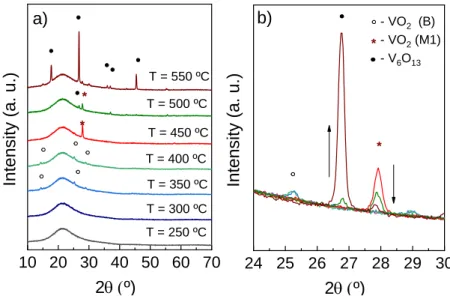
2To produce the monoclinic phase of VO2 thin films of amorphous VOx were e-beam evaporated using VO2 pellets. Preliminary studies were performed to assesses the specific conditions that allows the formation of VO2 monoclinic phase using annealing process at different temperatures and with a pressure of 250 mbar in a N2 atmosphere in a Rapid Thermal Annealing system (RTA) AS-One RTP System. From this study it was possible to conclude that 450 °C was the temperature that allowed to produce VO2 monoclinic phase. The XRD scans performed on quartz substrates and at different annealing temperatures are presented in Figure 3.
10 20 30 40 50 60 70
24 25 26 27 28 29 30
- VO2 (B) - VO2 (M1) - V6O13 *b)
* T = 550 ºC T = 500 ºC T = 450 ºC T = 400 ºC T = 350 ºC T = 300 ºCInt
ensity (
a.
u.)
2q (º)
T = 250 ºC *a)
*Int
ensity (
a.
u.)
2q (º)
Figure 3 - XRD scans of Vox films deposited on quartz samples annealed at different RTA temperatures in
a N2 atmosphere a) wide range scans showing the formation of VO2(B) at 300 °C, VO2(M) at 450 ºC and
V6O13 at 500 ºC b) zoomed region to highlight the changes.
As it can be seen, the as deposited sample is amorphous and with increasing temperature the crystallization is promoted. Due to lack of oxygen, during the thermal treatment the films tend to keep the VO2 stoichiometry of the evaporation pellets. For RTA treatments at 350 ºC and 400 ºC, the appearance of peaks at 2θ values of 14.4 °, 25.3 ° and 29.1 ° that can attributed to the (001), (110) and (002) planes of a monoclinic phase with the space group C2/m (ICSD #01– 081–2392), which does not present the reversible temperature induced transition. This phase is usually found and is commonly referred as VO2 (B).
At 450 °C a sharp peak located at 27.8° (indicated by an asterisk) is attributed corresponding to the (011) plane of monocline phase VO2 (M) with space group P21/C (ISCD #01-072-0514), being this the desired phase that presents the metal-to-insulator transition. Annealing at higher temperatures induces the formation of another phase V6O13 that is a monoclinic structure (space group C2/m, ICSD #01-075-1140) is known and usually used in batteries as a cathode material [24]. The increase of temperature led to the conversion of VO2(M) to V6O13 as can be
8
seen by the decrease of (011) main peak of VO2 and by the increase of the (110) peak plane. The as can be seen in Figure 8b). At 600 °C, the film is decomposed.
These results show how vanadium oxides can present very similar structures, and that the optimal condition must be very well tuned in order to form the specific VO2(M) phase. In this work, an optimal temperature of 450 ºC was attained in a N2 atmosphere.
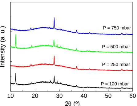
The optimization of the pressure in the annealing process at 450 °C in a N2 atmosphere during 300 s with a heat ramp of 50 °C/s was also performed. For this test 4 different pressure conditions during the thermal treatments were made, 100 mbar, 250 mbar, 500 mbar and 750 mbar and XRD scans can found on the following Figure 4.
20
30
40
50
60
- VO2 (B) - VO2 (M) P = 750 mbar P = 500 mbar P = 250 mbarInt
ensity (
a.
u.)
2q (º)
P = 100 mbar*
*
*
*Figure 4 – RTA test with different pressure conditions on Corning glass
This test (Figure 4) was made with a Corning substrate and it is possible to conclude that the pressure of N2 in the chamber have effect in the crystallization of the VO2 thin film. For high pressures, there are several peaks other than the expected one from the VO2 and a mixture of different phases are present.
The same test was made with a substrate with the VO2 thin film in the top and a TCO (in the case ITO) in the bottom and the same conclusion were obtained (Figure 5). The best condition of pressure is 250 mbar of N2 in the chamber.
9
10
20
30
40
50
60
Int
ensity (
a.
u.)
2q (º)
P = 750 mbar P = 500 mbar P = 250 mbar P = 100 mbarFigure 5 – XRD scans of ITO coated samples under different RTA pressure conditions.
It is possible to observe that for the pressure of 100 mbar and 500 mbar there are some peaks at 12° of 2θ, that do not correspond to the VO2 but that indicate the formation of a different phase. In these samples a C contamination was detected possibly due to the evaporation process where the misalignment of the electron beam lead to evaporation of the graphite crucible along with VO2.
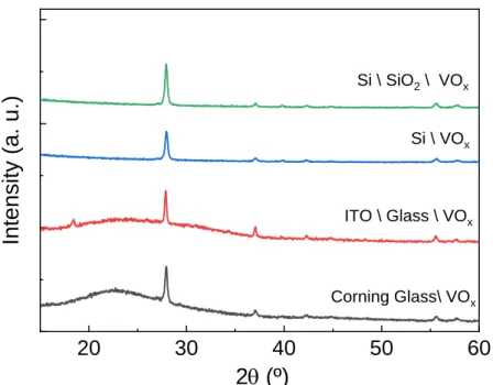
Comparing all the substrates used in the work, it is possible to conclude that glass substrate with ITO is the best option to use in the final sample, due to have a good crystallization of the VO2, it is transparent and already have the TCO build in from factory, that gives at least one less step in the fabrication process.
Due to the presence of some peaks not attributed to VO2 phases, an essay in different substrates was also tested (Figure 6) due to the fact that as already been reported that the crystallization of VO2 is sensitive to the substrate used [25].
10
20
30
40
50
60
Si \ SiO2 \ VOxInt
ensity (
a.
u.)
2q (º)
Si \ VOx ITO \ Glass \ VOx Corning Glass\ VOxFigure 6 – XRD scans on VO2 deposited in different substrates at a 250 mbar N2 pressure in the RTA system.
Comparing different substrates, a pressure of 250 mbar there is no significant difference as can be seen in Figure 6, so the best choice is still the option with ITO underneath the glass, for the its transparency and for having already the TCO from factory.
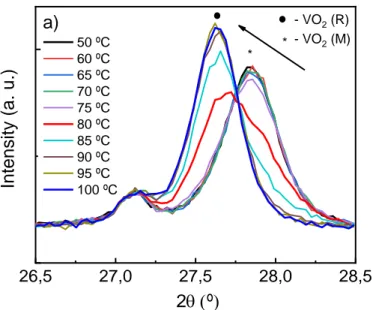
3.1.2 Phase change Transition
In order to confirm the reversibilityof the phase change of VO2 the sample produced with the same RTA specifications at 250 mbar, was tested inside the heating chamber of PANalyticalX’Pert Pro X-ray diffractometer, where it was heated from 50 C to 100 °C in 5 °C steps and then cooled from 100 °C to 30 °C, also with 5 °C steps. For each temperature 5 measurements were performed around the VO2 main peak position, between 25.5 ° and 28.5 ° of 2θ, using a step size of 0.0334 ° of 2θ.
11
26,5
27,0
27,5
28,0
28,5
*Int
ensity (
a.
u.)
2q (º)
50 ºC 60 ºC 65 ºC 70 ºC 75 ºC 80 ºC 85 ºC 90 ºC 95 ºC 100 ºCa)
- VO2 (R) - VO2 (M) *Figure 7 – XRD in-situ scans: Heating of the VO2 thin film on a Si Substrate
It is notorious in the Figure 7 a change in the XRD measurement to the different temperatures when heating the VO2 thin film, this shows that there is a phase change when changing the temperature and that the annealing process conditions were correct to obtain a VO2 thin film. The conditions were 450 °C during 300 s with a heat ramp of 50 °C/s and with a 250 mbar N2 pressure. 26,5 27,0 27,5 28,0 28,5
Int
ensity (
a.
u.)
2q (º) 100 ºC 95 ºC 90 ºC 85 ºC 80 ºC 75 ºC 70 ºC 65 ºC 60 ºC 55 ºC b) * * - VO2 (R) - VO2 (M)Figure 8 – Colling of the VO2 thin film on a Si Substrate
During the same process, but this time, cooling the sample from 100 °C to 50 °C presented on Figure 8, it is possible to conclude that there a phase change, but this time, to the initial structure, this means that the produced VO2 presents a reversible phase change.
12 26,5 27,0 27,5 28,0 26,5 27,0 27,5 28,0 28,5
Int
ensity (
a.
u.)
2q (º)
50 ºC 60 ºC 65 ºC 70 ºC 75 ºC 80 ºC 85 ºC 90 ºC 95 ºC 100 ºCa)
*2q (º)
100 ºC 95 ºC 90 ºC 85 ºC 80 ºC 75 ºC 70 ºC 65 ºC 60 ºC 55 ºCb)
* * - VO2 (R) - VO2 (M)Figure 9 – a) Heating of the VO2 thin film on a Si Substrate b) Colling of the VO2 thin film on a Si Substrate
In Figure 9 it is possible to conclude that there is a phase change with a temperature stimulus applied and this phase change is reversible.
3.1.3 Structural characterization using the Multipurpose Holder
Knowing the processing conditions required to produce VO2 thin films, the same protocol was used in glass coated with ITO substrates. The idea was to test the temperature control system (explained in more detail in section 3.3) and the 3D printed holder, in order to characterize in-situ the MIT transition in the XRD system and using the Arduino to control the temperature. The first testes showed a gradient heating effect possible due to the connector, as can be seen in Figure 10.
13
This gradient effect means that the temperature is not uniform along the sample surface. To confirm that the sample had different temperatures in different spots, the thermocouple was putted in several places confirming different temperatures.
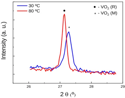
Nevertheless, it was possible to test the holder inside the X-ray diffractometer, by placing the thermocouple near the spot measured by the equipment. The resulted scans at different temperatures are presented in Figure 11.
26 27 28 29
Int
ensity (
a.
u.)
2 q (º)
30 ºC 80 ºC * - VO2 (R) - VO2 (M) *Figure 11 – XRD scans of VO2 films where the temperature was controlled using the Arduino setup and the
ITO resistor and the sample was mounted on the multipurpose holder.
In Figure 11, it is possible to observe the phase change in the VO2 thin film, with two measures, one at 30 °C and the other at 80 °C, so it proves that the holder used and the system develop to heat and control the sample temperature works and it does not interfere in the measurement. By controlling the temperature using the Arduino it was possible to testify the reversillity of the transition although a uniform heating cannot be insured.
To minimize the temperature gradient shown, the ITO film can be etched and patterned.
3.2 Electrical characterization of VO
2films
To characterize the transition, the samples were tested in a semiconductor parameter analyser to obtain the electrical resistance of the films. As a first step, this characterization was performed using the in-build heating stage of Agilent and electrical contacts were deposited in VO2 thin films to allow the extraction of I-V curves.
3.2.1 Electrode Mask design
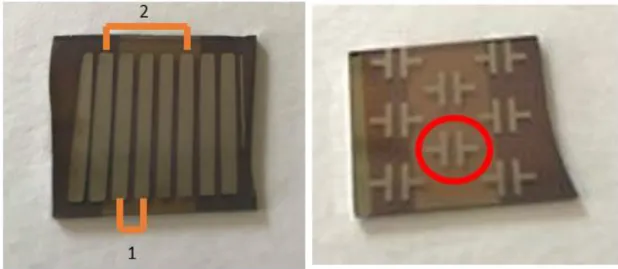
To perform the electrical characterization, two different electrical contacts designs were used, one in a “T” shape and another having vertical stripes. The first design was used because
14
shadow masks were already available, and the second design was developed during this work to optimized in the implementation in the multipurpose holder using the Edgecard Connector assembly.
.
Figure 12 – Design of the Vertical stripes design mask produced
This second design, (shown in Figure 12) was drawn in Adobe Illustrator and it was cut in PET substrates to produce shadow masks using the CO2 infrared cutting system (Universal Laser System) with 10 W of power and 0.254 m/s of speed
3.2.2 Electrical Test
The tests were performed in Agilent 4155C semiconductor parameter analyzer connected to a Cascade Microtech M150 manual microprobe station, controlled by the software Metrics ICS, using the heat plate of the equipment, from 25 °C to 100 °C in 5 °C steps. In each measurement a potential sweep from -1.5 V to 1.5 V with 61 point, measuring the current and extracting the resistance at each temperature. In the vertical stripes design two measurements were performed at two different pairs of electrodes to test the different distance between electrical contacts as shown in Figure 13. It the “T” shape design two measurements were also performed to observe the reproducibility of the electrical changes in the VO2 thin film.
Figure 13 - On the left side vertical stripes design with two distance marked corresponding to the electrodes used during the electrical characterization. On the right side “T” shape design with a mark
15
In the design of Figure 13, the distance marked as “1” has 0.6 mm of separation between electrodes and the distance marked as “2” is 9.1 mm. The two measures in the “T” shape design were made in the marked spot at the Figure 13. The two measures were made to observe if the contacts between the two measure contacts have any influence in the measure.
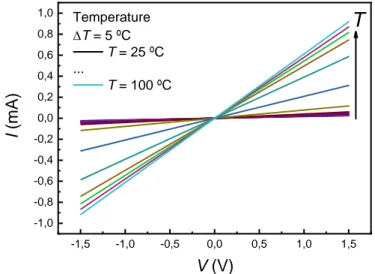
The Figures 14 and 15 shows the values measured at the distance of 0.6 mm, being evident that there are straight lines, an ohmic behavior in the range of -1.5 V and 1.5 V.
-1,5 -1,0 -0,5 0,0 0,5 1,0 1,5 -1,0 -0,8 -0,6 -0,4 -0,2 0,0 0,2 0,4 0,6 0,8 1,0 Temperature DT = 5 ºC T = 25 ºC ... T = 100 ºC
I (
mA)
V (V)
T
Figure 14 – I-V measurements performed at different in increasing Temperatures using contacts 0.6 mm spacing -1,5 -1,0 -0,5 0,0 0,5 1,0 1,5 -1,0 -0,8 -0,6 -0,4 -0,2 0,0 0,2 0,4 0,6 0,8 1,0 Temperature DT = 5 ºC T = 100 ºC ... T = 25 ºC
I (
mA)
V (V)
T
Figure 15 - I-V measurements performed at different in decreasing temperatures using contacts 0.6 mm spacing
The measurements performed using the Agilent heating stage allowed to confirm the quality of the MIT transition as can be seen in Figure 16.
16 20 30 40 50 60 70 80 90 100 0 2 4 6 8 10 12 14 16 18 20 R (k W ) Temperature (ºC) Increasing temperature Decreasing temperature
Figure 16 – Resistance evolution of VO2 thin films for different heating temperatures using the Vertical stripes
design, with a contact spacing of 0.6 mm
In the first test (Figure 16) it is possible to observe a decrease resistance with the increasing of the temperature. The resistance changes a lithe more than 1 order of magnitude, from near 20 kΩ in the low temperature regime (monoclinic phase and “insulator” behavior) to a resistance of near 800 Ω in the high temperature regime. The transition also presents a hysteresis. For all measurements performed, it was observed the same ohmic behavior showed on Figures 14 and 15. 20 30 40 50 60 70 80 90 100 110 0 10 20 30 40 50 60 70 80 R (k W ) Temperature (ºC) Increasing temperature Decreasing temperature
Figure 17 – Resistance evolution of VO2 thin films for different heating temperatures using the Vertical stripes
design, with a contact spacing of 9,1 mm. For this second distance, the resistance drop is more significate due to the increasing distance between contacts.
The same test was performed using another pair of electrodes with different spacing as can be seen in Figure 17.
17 20 30 40 50 60 70 80 90 100 110 0 10 20 30 40 50 60 70 R (k W ) Temperature (ºC) Increasing temperature Decreasing temperature
Figure 18 – Resistance evolution of VO2 thin films for different heating temperatures using the “T” shape
electrode design.
The Figure 18 shows the test performed on the “T” shape and as expect, it is notorious the electrical change with the temperature difference.
40 50 60 70 80 0 10 20 30 40 50 60 R (k W ) Temperatura (ºC) Increasing temperature Decreasing temperature
Figure 19 - Cycle test in "T" shape design
It is possible to conclude that in all shapes a decrease of the resistance with the increasing of temperature and it possible to observe that for a temperature around 65 °C there is two distinguish states, making this a great solution for switch, for instance a “on state” and a “off state”.
18
The cycle test (Figure 19) shows that the VO2 thin film resistance change is reproducible.
3.3 Temperature Controller development
3.3.1 Circuit development
In order to measure and control the temperature of VO2 thin film, an electrical circuit was designed. The brain for this circuit was an Arduino Uno which receive the temperature information from the circuit and with a PID function, the Arduino will decide if is necessary to increase or decrease the temperature and the amount needed to reach and maintain the temperature around the wanted Set Point.
The circuit has an IC (AD595) that will get the temperature information from a type K thermocouple and this reading will be send to the Arduino as a voltage value, that for this IC specific case o is 10 mV/°C. To protect the IC, a short circuit with a 10 kΩ resistor from pin 1 of the IC and the ground was introduced. In this pin is also connected the positive side of the thermocouple and the negative side is connected do pin 14. To power the IC, we can use a voltage between 5 V and 30 V, connected to the pin 11. The pins 4, 7 and 13 are connected to ground. The pins 8 and 9 have a short circuit between them and the voltage in there is the temperature information for the Arduino, the rest of the pins were unconnected. The schematic of these connections made in Eagle® Software is shown in Figure 20.
Figure 20 - Schematic of the Temperature controller setup
After processing that information through the PID function, the Arduino will control the amount of current in the thin film resistor with the PWM function, with a square wave output that gives 5 V in the maximum peak and 0 V at the lower peak. This PWM, function connected to a transistor (N-channel enhancement mode power MOS – IRF520) can act like a switch, controlling the amount of current in the thin film resistor under the substrate. The drain is connected to one side of the thin film resistor of the substrate (while the other contact is connected to the power
19
supply), the source is connected to ground and the gate is connected to a 330 Ω resistor that is connected to the PWM of Arduino (schematic in Figure 21). This purpose of this resistor is to protect the Arduino form unwanted and unexpected current that main damage the equipment.
Figure 21 - Schematic of the transistor with the sample
The thermocouple is connected to the circuit through a thermocouple plug and the all the connections with the sample is made with an Edgecard Connector with 20 pins, 10 for each side of the substrate. To connect the power supply in the system and to extract the electrical data from the sample out of the PCB, there are pin headers. In order to have the capability to turn off the circuit, it has two switches.
To design the circuit the software Eagle was used.
3.3.2 PCB development
Regarding the PCB specifications, there are no limitations on the size of the board, but there are a few details to consider such as the location of the components and the width of the traces. The Edgecard Connector should be on one of the edges of the board (so that the sample doesn’t have anything under), the Pin Headers must be placed in a way, so that itis possible to connect wires, the thermocouple plug needs to be the closest possible to the IC and the switches must have some room to be operable. The traces width choose to the PCB is 6 mil (mil is a unit used in PCB software and industry, being 1 mil equal to 1/1000 of the inch or 25.4 µm), that is enough to hold almost 1 A, more than the system reach. The thickness of the PCB is 1 mm, the manufacture offers several sizes of PCB, but this parameter does not have effect on the outcome of the system, so it has chosen a size not too big and no too small to fit well in the holder. The PCB, shown in Figure 22 is 77.47 mm by 54.61 mm.
20 Figure 22 - PCB Layout without the ground planes and the vias.
Ground plane in booth sides of the PCB and several vias along the board to connect booth ground planes were projected. The vias will ensure a proper grounding of the circuit.
To design the PCB, the software Eagle. Pictures of the Pin Headers, the EgdeCard Connector and the PCB are available in Appendix A.
The ordered PCB was successfully build with all components soldered.
3.3.3 Arduino
The Arduino is the main part of the electrical system, being responsible to read the temperature and control the temperature of the sample. For this, a code was developed, that will work in all the Arduino types. The one used was the Arduino Uno, from a third-party supplier, but this condition will not affect the outcome of the project.
The signal from the AD595 will enter the Arduino in an analog port, after that, it is converted to a temperature value and a smoothing function to give a constant and accurate temperature reading. With this reliable value it is applied a Proportional-Derivate-Integral (PID) function, this is the function that decides if the system needs to be heated or cooled through a Pulsed-Width Modulation (PWM) function that have and exit in certain digital port (the ones with the “~” sign). The system has a changing Set Point function that can be turned on or off by the user, when turned on, the Arduino will change the Set Point of the system with the increment intended by the user after a desired time, also chosen by the user. The code is provided in Appendix B.
The Arduino software is called IDE and can shows the actual temperature of the sample and the Set Point in two form, numerical and graphical (Appendix C).
The code is prepared to have an LCD display with sixteen characters by two lines, with an I2C module. This module will reduce the sixteen connections to four, being these four
21
connections, a 5 V, a ground (GND), a serial clock line (SCL) and serial data line (SDA) ports. The SCL will connect to the analog port 5 and the SDA will connect to the analog port 4. The display is programed to show the actual temperature read, the Set Point, the increment and the time per Set Point chosen by the user.
In Figure 23 a reading on the LCD is displayed as an example of the information retrieved by the Arduino code.
Figure 23 - LCD display with temperature, Set Point, increment and time information
It is available in Appendix D, a brief explanation of the IC used and a brief explication about the Arduino and the functions used in the code developed.
3.4 Multipurpose Holder development
The holder was developed in a “T” shape where the narrow part is the one that fits in the x-ray diffractometer. The holder is fixed to the XRD prefix, and the sample is fixed to the holder using the Edgecard connectors. The central part of the holder has a hole, to allow in the future to perform optical characterizations in the VO2 sample. In the larger part of holder, there is a small salience to fix the Egdecard Connector. With the same width of the larger part of the holder, there is a loose piece with the same salience of the holder to be able to fit in the top part of the Egdecard Connector and to fix it (this connector is symmetrical, and this feature makes possible to have the same salience size in booth pieces).
The design of the holder is presented in Figure 24 and the printer holder is presented in Figure 25.
The two pieces will fit in each other with the help of two screw and two nuts, one on each side, making the Edge Connector fixed during all measurements. The nuts will fit in the loose piece and the screws will go through the holder and will be hidden so the bottom part can be flat in order to be balanced in flat surfaces of several equipment.
22 Figure 24 - Multipurpose Holder Design
The holder showed on Figure 24, has a length of 60.2 mm and a width of 42.9 mm. The segment that fits the XRD is 35.0 mm and a height of 10.4 mm. The loose piece has the same length of the holder but have a width of 12.9 mm and a height of 7.0 mm. A picture of the holder with the Edgecard Connector is showed on Figure 25.
Figure 25 - Holder with the Edgecard Connector
The holder was designed and projected in Fusion 360 and it was printed in the 3D printing Ultimaker 2 +, using a PLA compound, with an infill of 18%, a nozzle of 0.4 mm, a resolution of 0.15 mm, without the need of support. Several versions of the holder were designed, in order to correct the dimensions and the alignment of the samples. The versions evolution is in Appendix E by chronologic order. Pictures of the holder fitted on the XRD is in Appendix F.
23
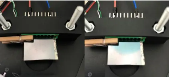
A photograph of the developed multipurpose holder is shown (figure 26), with the produced PCB mounted on the back of the holder and set on the XRD system.
The PCB, the sample, a power source and the Arduino are kept inside the XRD fixture, having connections to a PC externally in order to allow the control of the heating element. As a reference two different temperatures (T1 = 30 ºC and T2 = 100 ºC) are highlighted corresponding to a heating command from T1 to T2 with the Arduino code while the sample was continually scanned with x-rays.
Figure 26– Final holder with the produced PCB. Diffractograms are also visible to show the structural properties of the films while the sample temperature is increased from 30 to 100 ºC using the controller and the Arduino board.
It is possible to see the shift in the peak position while heating the sample, from 30 ºC to 100 ºC (corresponding to the scan more shifted to lower 2θ angles).
The PCB have included connections to perform in the future the extraction of the electrical characteristics of the samples, having contacts deposited on top. These measurements can be performed using a precision multimeter.
3.5 Electrical contacts optimization
After confirming that the system worked, a sample optimization was needed in order to do simultaneous characterization and correct some problems, like the gradient effect when heating. In order to perform the simultaneous characterization, a new mask (Figure 27) was
27,5 28,0 28,5 T1 = 30 ºC T2 = 100 ºC
Intensity (a.u.
)
2q (º)
24
designed with eight stripes with 20 mm in length, being the lower part always the same size, 0.7 mm width and separated apart for each other 1.95 mm, so each stripe can connect to the Edge Connector individually. In the top part of the design, each stripe has 1 mm width and they have three different distance from each other, being this distance 0.5 mm, 1 mm and 1.5 mm, being this distance the same for each mask.
Figure 27 - Mask distance of 1 mm for electrical characterization
To prevent a short circuit between the stripes in the bottom part of the design and the Egdecard Connector, assuring that one contact stays connected with only one stripe for a better measure and to guarantee that there is no short circuit between the upper part and the bottom part of the sample through the sides, a simple mask were made, a rectangle with 20 mm by 10 mm. This mask is for the VO2 thin film depositing process and it is placed in the upper part of the electrical design ensuring that the thin film do not reach the boarders of the sample and the bottom part of the electrical design.
To have a better deposition of the metal contacts on the bottom part of the sample, a mask was made with two vertical stripes, with 20 mm in length and 5 mm in width, distance from each other 10mm. All the masks were made in Al.
In order to avoid the gradient effect observed, an etching process was made in the ITO, using the CO2 infrared cutting system (Universal Laser System) with 25 W of power and 0.254 m/s of speed. This process was performed before every other process and it was made in the lower part of the sample, in the part that connects to the Edgecard Connector to ensure that the current will only flow in the top part of the sample, that will assure that if the gradient effect persist to exist, it will be minimized and the temperature reading will be more accurate.
25
Chapter 4: Conclusions and future perspectives
Besides the goal of this project is not the optimization of the VO2 thin films, a condition was determined, that does gives a VO2 with some impurities, but it is VO2 and it was possible to observe the phase change at 68 °C. The conditions of RTA are 450 °C, with a heat ramp of 50 °C, after achieving the temperature, it stays during 300 s with 250 mbar N2 atmosphere. Further studies may conclude better conditions to the fabrication of the VO2.
The electrical tests proved what were expected, two different states, a metal state and an insulator state and at around 65 °C, depending if the thin film is being heated or cooled, produce two different levels, that can be transformed into to switch states, an on state and an off state.
A holder was developed, fitted well in the equipment, especially in the X-Ray Diffraction system present in the CENIMAT laboratories. Besides that, a PCB was developed at the end and tested in the XRD. Although it was not possible to perform a simultaneous test due to contact problems as the Mo contacts were oxidized at the latest tests. New samples are required.
In the future, to prevent the gradient effect situation, some new procedures must be taken, for example, have the same size of TCO as the VO2 and they are being aligned through the substrate. This process can be done by a better etching process or a by doing a deposition of the TCO using the mask used to deposit de VO2 thin film.
It now can start to be tested in others equipment’s, for instance, the Atomic Force Microscope or the ellipsometer, to get the most information possible, always with the same conditions
A new temperature measuring system can be done, replacing the one created. The new system can have an infrared temperature measuring system, this will promote less contact with the sample (less change of contamination) and a more precise read if the gradient effect persists to exist.
To improve the user experience, a program in some sort of programing language can be made, with the possibility to change the temperature Set Point, the increment, the cycle time, change the PID constants. Can also have the actual read of the temperature. This is helpful if the user is not comfortable programing or does not know how to program the Arduino.
27
References
[1] F. J. Morin, “Oxides which show a metal-to-insulator transition at the neel temperature,” 1959, Phys. Rev. Lett., vol. 3, no. 1, pp. 34–36.
[2] T. C. Koethe et al., “Transfer of spectral weight and symmetry across the metal-insulator transition in VO2,” 2006, Phys. Rev. Lett., vol. 97, no. 11, pp. 1–4.
[3] M. Jiang et al., “Room Temperature Optical Constants and Band Gap Evolution of Phase Pure M1 VO2 Thin Films Deposited at Different Oxygen Partial Pressures by Reactive Magnetron Sputtering,” 2014, J. Nanomater., vol. 2014, pp. 1–6.
[4] Y. Gao et al., “Nanoceramic VO 2 thermochromic smart glass: A review on progress in solution processing,” 2012, Nano Energy, vol. 1, no. 2, pp. 221–246.
[5] F. Béteille and J. Livage, “Optical Switching in VO2 Thin Films,” 1998, J. Sol-Gel Sci. Technol., vol. 921, pp. 915–921.
[6] J. Nag and R. F. Haglund Jr, “Synthesis of vanadium dioxide thin films and nanoparticles,” 2008, J. Phys. Condens. Matter, vol. 20, no. 26, p. 264016.
[7] C. H. Griffiths and H. K. Eastwood, “Influence of stoichiometry on the metal-semiconductor transition in vanadium dioxide,” 1974, J. Appl. Phys., vol. 45, no. 5, pp. 2201–2206. [8] A. A. Akande et al., “Phase evolution of vanadium oxides obtained through temperature
programmed calcinations of ammonium vanadate in hydrogen atmosphere and their humidity sensing properties,” 2015, Mater. Chem. Phys., vol. 151, pp. 206–214.
[9] N. Bahlawane and D. Lenoble, “Vanadium oxide compounds: Structure, properties, and growth from the gas phase,” 2014, Chem. Vap. Depos., vol. 20, no. 7–9, pp. 299–311. [10] Y. Zhang, “VO2(B) conversion to VO2(A) and VO2(M) and their oxidation resistance and
optical switching properties,” 2016, Mater. Sci. Pol., vol. 34, no. 1, pp. 169–176.
[11] C. Leroux, G. Nihoul, and G. Van Tendeloo, “From to Theoretical structures of polymorphs and in situ electron microscopy,” 1998, Phys. Rev. B - Condens. Matter Mater. Phys., vol. 57, no. 9, pp. 5111–5121.
[12] P. Kiria, G. Hyett, and R. Binionsa, “Solid state thermochromic materials,” 2010, Adv. Mater. Lett., vol. 1, no. 2, pp. 86–105.
[13] D. Alie et al., “Direct synthesis of thermochromic VO2 through hydrothermal reaction,” 2014, J. Solid State Chem., vol. 212, pp. 237–241.
[14] G. Fu, A. Polity, N. Volbers, and B. K. Meyer, “Annealing effects on VO2 thin films deposited by reactive sputtering,” 2006, Thin Solid Films, vol. 515, no. 4, pp. 2519–2522. [15] J. B. K. Kana et al., “Thermochromic VO 2 thin films synthesized by rf-inverted cylindrical
magnetron sputtering,” 2008, Appl. Surf. Sci., vol. 254, no. 13, pp. 3959–3963.
[16] G. Xu and P. Jin, “Related content Formation and Thermochromism of VO 2 Films Deposited by RF Magnetron Sputtering at Low Substrate Temperature,” 1994, Jpn. J. Appl. Phys., vol. 33, p. 1478.
[17] J. F. De Natale, P. J. Hood, and A. B. Harker, “Formation and characterization of grain-oriented VO2 thin films,” 1989, J. Appl. Phys., vol. 66, no. 12, pp. 5844–5850.
28
[18] M. H. Lee and M. G. Kim, “RTA and stoichiometry effect on the thermochromism of VO2 thin films,” 1996, Thin Solid Films, vol. 286, no. 1–2, pp. 219–222.
[19] B.-G. Chae et al., “Highly Oriented VO[sub 2] Thin Films Prepared by Sol-Gel Deposition,” 2006, Electrochem. Solid-State Lett., vol. 9, no. 1, p. C12.
[20] Y. Liu, H. Tao, X. Chu, M. Wan, J. Bao, and X. Zhao, “Effects of addition of tungsten chloride on optical properties of VO 2-based thermochromic films prepared by sol-gel method,” 2014, J. Non. Cryst. Solids, vol. 383, pp. 116–120.
[21] A. Gonçalves et al., “Smart optically active VO2 nanostructured layers applied in roof-type ceramic tiles for energy efficiency,” 2016, Sol. Energy Mater. Sol. Cells, vol. 150, pp. 1–9. [22] L. Kang et al., “Effects of annealing parameters on optical properties of thermochromic VO2 films prepared in aqueous solution,” 2010, J. Phys. Chem. C, vol. 114, no. 4, pp. 1901–1911.
[23] A. Devices, “Monolithic thermocouple amplifiers a with Cold Junction Compensation,” 1997.
[24] H. Fei, Y. Lin, and M. Wei, “Journal of Colloid and Interface Science Facile synthesis of V 6 O 13 micro-flowers for Li-ion and Na-ion battery cathodes with good cycling performance,” 2014, J. Colloid Interface Sci., vol. 425, pp. 1–4.
29
Appendix A – Components used for the PCB development
Figure 28 - 15 male Pin Header used in the PCB with an one euro coin for size comparison
30
Appendix B
– Arduino code developed for temperature
control
#include <Wire.h> #include <LiquidCrystal_I2C.h> #define pSensor A0 #define resistor A1 #define pControlo 3const int numReadings = 100;
float readings[numReadings]; // the readings from the analog input
int readIndex = 0; // the index of the current reading
float total = 0; // the running total float average = 0; // the avarage float setPoint = 70; int ControloPwm = 127; double error = 0; double P=0, I=0, D=0; double kp=2, ki=4, kd=4; double PID; long lastProcess; float Derror = 0; float errorAnterior = 0; float time_reset = 0; float tempo = 0; float tt = 0; int i = 0; float increment = 5; float interval = 0; float timeM = 10; float margem = 1.5; float tempoR = 0; float somatempo = 0; int raw= 0; int Vin= 5; float Vout= 0; float R1= 10000; float R2= 0; float buffer= 0; LiquidCrystal_I2C lcd(0x27, 2, 1, 0, 4, 5, 6, 7, 3, POSITIVE); void setup() { Serial.begin(9600); lcd.begin (16, 2); lcd.setBacklight(HIGH); interval = timeM * 60; /*
Serial.println("Qual o Set Point desejado?"); while (Serial.available()==0){}
setPoint = Serial.parseInt(); */
pinMode(pSensor,INPUT); pinMode(pControlo, OUTPUT); for (int thisReading = 0; thisReading < numReadings; thisReading++) { readings[thisReading] = 0; }
31 }
void loop() {
int ValorSensor = analogRead(pSensor); float voltage = ValorSensor * (5.0 / 1023.0); float Celsius = voltage*100;
total = total - readings[readIndex]; readings[readIndex] = Celsius; total = total + readings[readIndex]; readIndex = readIndex + 1; if (readIndex >= numReadings) { readIndex = 0;
}
average = total / numReadings;
/* //Serial Reader if (Serial.available() > 1) setPoint = Serial.parseInt(); */ //PID
error = setPoint - average;
float deltaTime = (millis() - lastProcess) / 1000.0;
lastProcess = millis(); Derror = error - errorAnterior; errorAnterior = error;
//P
P = error*kp;
//I
I = I + (error * ki) * deltaTime; I = constrain (I, -255, 255); //D D = Derror* kd / deltaTime; //PID PID = P + I + D; // conversor de saída
ControloPwm = constrain (PID, 0, 255);
//timer
if ((average > setPoint - margem) && (average < setPoint + margem)) {
tt = (interval / deltaTime); i= i + 1;
Serial.print("timer activo"); Serial.print("\t");
somatempo = somatempo + deltaTime; tempoR = interval - somatempo;
}
if (i > tt) {
setPoint = setPoint + increment; Serial.print("SetPoint mudou"); Serial.print("\t"); i = 0; somatempo = 0; } else
32 { } analogWrite(pControlo, ControloPwm); Serial.print(average); Serial.print("\t"); Serial.println(setPoint); /*Serial.print("\t"); Serial.println(ControloPwm/5); Serial.print("\t"); Serial.print(millis()); Serial.print("\t"); Serial.print(tt); Serial.print("\t"); Serial.print(i); Serial.println("\t"); */ lcd.setCursor(0, 0); lcd.print("T="); lcd.print(average); lcd.setCursor(8, 0); lcd.print("SP="); lcd.print(setPoint); lcd.setCursor(0, 1); lcd.print("I="); lcd.print(increment); lcd.setCursor(7, 1); lcd.print("Tm="); lcd.print(tempoR); delay(10); }
33
Appendix C
– Monitor Series and Plotter Series from
Arduino Software
Figure 31 - Monitor Series from the Arduino software with two columns, the one from the left is the actual temperature and the right one, the Set Point
Figure 32 - Plotter Series from the Arduino software with two lines, the blue one is the actual temperature and the red one is the Set Point
![Figure 1 – Schematic V-O phase diagram with the Magnéli series (V n O 2n+1 ) highlighted in blue and the Wadsley series (V n O 2n-1 ) highlighted in green [9]](https://thumb-eu.123doks.com/thumbv2/123dok_br/15463799.1031837/24.892.252.689.666.989/figure-schematic-diagram-magnéli-series-highlighted-wadsley-highlighted.webp)