Transparent Oxide
Thin-Film Transistors:
In partial fulfillment of the requirements
for the degree of Doctor of Philosophy
in Nanotechnologies and Nanosciences,
by Universidade Nova de Lisboa,
Faculdade de Ciências e Tecnologia
Lisboa, 2010
Pedro Miguel Cândido Barquinha
©
Copyright by Pedro M. C. Barquinha August , 2010
T
T
r
r
a
a
n
n
s
s
p
p
a
a
r
r
e
e
n
n
t
t
O
O
x
x
i
i
d
d
e
e
T
T
h
h
i
i
n
n
‐
‐
F
F
i
i
l
l
m
m
T
T
r
r
a
a
n
n
s
s
i
i
s
s
t
t
o
o
r
r
s
s
:
:
p
p
r
r
o
o
d
d
u
u
c
c
t
t
i
i
o
o
n
n
,
,
c
c
h
h
a
a
r
r
a
a
c
c
t
t
e
e
r
r
i
i
z
z
a
a
t
t
i
i
o
o
n
n
a
a
n
n
d
d
i
i
n
n
t
t
e
e
g
g
r
r
a
a
t
t
i
i
o
o
n
n
In
partial
fulfillment
of
the
requirements
for
the
degree
of
Doctor
of
Philosophy
in
Nanotechnologies
and
Nanosciences,
by
Universidade
Nova
de
Lisboa,
Faculdade
de
Ciências
e
Tecnologia
ACKNOWLEDGMENTS
Besides the personal effort made during countless days and nights of work, sometimes leading to
frustrating results, others to exciting paths to move forward (after all, as happens with any research
work), all this would never be possible without the guidance and support of a large number of
persons. From these, I would like to highlight and sincerely thank:
To Prof. Elvira Fortunato and Prof. Rodrigo Martins. I am proud and grateful for having them as the
advisors of this research work. From the moment they allowed me to work in their research group, I
had their full support and guidance. With their giant efforts, expertise and passion for science, they
built fully equipped laboratories and established crucial relations with national and international
partners, creating the scientific and financial basis that allowed this and many other research works
to be developed. I also thank them for their confidence in my work and for their great investment in
my personal and academic formation, for instance by including me in important research projects
and by allowing me to participate in a large number of important scientific conferences throughout
the world. I hope that the results obtained after these years meet their expectations. Sincerely, thank
you both!
To Dr. Luís Pereira and Ing. Gonçalo Gonçalves, friends and partners of endless lab work, travels
discussions, meetings and beer sessions. Their persistence, knowledge and ideas (even the craziest
ones) helped to surpass a large number of difficulties found during this and other works. Everything
is turned much easier having friends like them on our side!
To Prof. Hugo Águas, for his friendship and for helping me with his large expertise and knowledge on
material science and characterization tools. Together with my passion for music and technology, he is
the responsible for making me spend money in audiophile equipment (for the madness of my wife)!
To past and present co‐workers: Prof. Isabel Ferreira, Dr. Leandro Raniero, Ing. António Marques, Ing.
Luís Tomás, Ing. Nuno Martins, Ing. Daniel Costa, Ing. Lúcia Gomes, , Ing. Alexandra Gonçalves, Ing.
Sónia Pereira, Ing. Nuno Correia, Ing. Cláudia Costa, Dr. Elangovan Elamurugu, Ing. Vitor Figueiredo,
Ing. Leonardo Silva, Ing. Rita Albuquerque, Dr. Joana Pinto, Msc. Raquel Barros, Ings. Pawel and
Iwona Wojcik and others that probably I did not mention. Working directly or indirectly with me, all
of them definitively helped me to reach here. Thank you all!
To Manuel Quintela, Joel Figueiredo and Carlos Alcobia for their large expertise and help solving all
To the partners of Multiflexioxides, an European project developed during the period of the research
work of this dissertation. Among all the partners, I would like to highlight Prof. Anna Vilà, Dr. Antonis
Olziersky and Prof. Joan Morante from Universitat de Barcelona, for the structural, morphological
and compositional analysis of most of the thin films presented in this dissertation; Prof. Marija Kosec
and Prof. Danjela Kuscer from Josef Stefan Institute for processing some of the oxide semiconductor
and dielectric targets used for sputtering deposition; Dr. Lorraine Byrne from Hewlett‐Packard
(Manufacturing) Limited, Dublin and Dr. John Rudin from Hewlett‐Packard Laboratories, Bristol for
the integration of the active matrix backplanes with the liquid crystal frontplanes.
To Prof. John Wager for allowing me to stay during some weeks at Oregon State University learning
and changing ideas with his research group. There I had the pleasure to meet and work with Dr. Hai
Chiang and Dr. David Hong, who did remarkable research on “Transparent Electronics” and warmly
received me at their houses, family and life during my stay in Oregon. Thanks for everything!
To “Fundação para a Ciência e Tecnologia”, for the fellowship and conference grants attributed
during this work, allowing me to do research as a full‐time job.
To “Fundação Calouste Gulbenkian” and “Fundação Luso‐Americana para o Desenvolvimento”, for
the grants to participate in international conferences.
To all my friends, for their support and comprehension and for understanding the personal
importance of my work and my lack of availability during the last years.
To my family: my family‐in‐law, Jacinto, Cesaltina, Cátia, João and Tiago, for supporting me and for
the unforgettable moments we spent together, for having me as part of their family and life; my
sister, father and mother, Ana, Martinho and Milú, for being such a great example for me, for all
their love and comprehension, for devoting their life to give me the best anyone could have. I own
them all that I am today!
To my wife, Ana. Words will never be enough to express how grateful I am of making part of her life.
Without her all this process would have been much harder, probably impossible. She fought really
hard to organize her and our life during these last years and her support, comprehension and love
were behind all the imaginable limits, keeping me strong during this stressful period. Thank you for
being the sun even on cloudy days, I hope to be yours now and show you it was worth the effort.
ABSTRACT
This dissertation is devoted to the study of the emerging area of transparent electronics,
summarizing research work regarding the development of n‐type thin‐film transistors (TFTs) based
on sputtered oxide semiconductors. All the materials are produced without intentional substrate
heating, with annealing temperatures of only 150‐200 °C being used to optimize transistor
performance. The work is based on the study and optimization of active semiconductors from the
gallium‐indium‐zinc oxide system, including both the binary compounds Ga2O3, In2O3 and ZnO, as well as ternary and quaternary oxides based on mixtures of those, such as IZO and GIZO with
different atomic ratios. Several topics are explored, including the study and optimization of the oxide
semiconductor thin films, their application as channel layers on TFTs and finally the implementation
of the optimized processes to fabricate active matrix backplanes to be integrated in liquid crystal
display (LCD) prototypes. Sputtered amorphous dielectrics with high dielectric constant (high‐κ)
based on mixtures of tantalum‐silicon or tantalum‐aluminum oxides are also studied and used as the
dielectric layers on fully transparent TFTs. These devices also include transparent and highly
conducting IZO thin films as source, drain and gate electrodes.
Given the flexibility of the sputtering technique, oxide semiconductors are analyzed regarding several
deposition parameters, such as oxygen partial pressure and deposition pressure, as well as target
composition. One of the most interesting features of multicomponent oxides such as IZO and GIZO is
that, due to their unique electronic configuration and carrier transport mechanism, they allow to
obtain amorphous structures with remarkable electrical properties, such as high hall‐effect mobility
that exceeds 60 cm2 V‐1 s‐1 for IZO. These properties can be easily tuned by changing the processing conditions and the atomic ratios of the multicomponent oxides, allowing to have amorphous oxides
suitable to be used either as transparent semiconductors or as highly conducting electrodes. The
amorphous structure, which is maintained even if the thin films are annealed at 500 °C, brings great
advantages concerning interface quality and uniformity in large areas.
A complete study comprising different deposition conditions of the semiconductor layer is also made
regarding TFT electrical performance. Optimized devices present outstanding electrical performance,
such as field‐effect mobility (µFE) exceeding 20 cm2 V‐1 s‐1, turn‐on voltage (Von) between ‐1 and 1 V,
subthreshold slope (S) lower than 0.25 V dec‐1 and On‐Off ratio above 107. Devices employing amorphous multicomponent oxides present largely improved properties when compared with the
ones based on polycrystalline ZnO, mostly in terms of µFE. Within the compositional range where IZO
contents favor large µFE but also highly negative Von, which can be compensated by proper amounts of zinc and gallium. Large oxygen concentrations during oxide semiconductor sputtering are found to
be deleterious, decreasing µFE, shifting Von towards high values and turning the devices electrically unstable. It is also shown that semiconductor thickness (ds) has a very important role: for instance, by
reducing ds to 10 nm it is possible to produce TFTs with Von≈0 V even using deposition conditions and/or target compositions that normally yield highly conducting films. Given the low ds of the films, this behavior is mostly related with surface states existent at the oxide semiconductor air‐exposed
back‐surface, where depletion layers that can extend towards the dielectric/semiconductor interface
are created due to the interaction with atmospheric oxygen. Different passivation layers on top of
this air‐exposed surface are studied, with SU‐8 revealing to be to most effective one. Other
important topics are source‐drain contact resistance assessment and the effect of different annealing
temperatures (TA), being the properties of the TFTs dominated by TA rather than by the deposition conditions as TA increases. Fully transparent TFTs employing sputtered amorphous multicomponent dielectrics produced without intentional substrate heating present excellent electrical properties,
that approach those exhibited by devices using PECVD SiO2 produced at 400 °C. Gate leakage current
can be greatly reduced by using tantalum‐silicon or tantalum‐aluminum oxides rather than Ta2O5. A
section of this dissertation is also devoted to the analysis of current stress stability and aging effects
of the TFTs, being found that optimal devices exhibit recoverable threshold voltage shifts lower than
0.50 V after 24 h stress with constant drain current of 10 µA, as well as negligible aging effects during
18 months.
The research work of this dissertation culminates in the fabrication of a backplane employing
transparent TFTs and subsequent integration with a LCD frontplane by Hewlett‐Packard. The
successful operation of this initial 2.8” prototype with 128x128 pixels provides a solid demonstration
that oxide semiconductor‐based TFTs have the potential to largely contribute to a novel electronics
era, where semiconductor materials away from conventional silicon are used to create fascinating
RESUMO
Esta dissertação é dedicada ao estudo da área emergente da electrónica transparente, resumindo o
trabalho de investigação relacionado com o desenvolvimento de transístores de filme fino (TFTs)
baseados em óxidos semicondutores depositados por pulverização catódica. Todos os materiais são
produzidos sem aquecimento intencional do substrato e os dispositivos são sujeitos a um tratamento
térmico final a apenas 150‐200 °C para optimização do seu desempenho. O trabalho é baseado no
estudo e optimização de semicondutores activos do sistema de óxidos de gálio‐índio‐zinco, incluindo
quer os compostor binários Ga2O3, In2O3 and ZnO, quer óxidos ternários e quaternários baseados em
misturas desses, como o IZO ou o GIZO com diferentes razões atómicas. São explorados diversos
tópicos, incluindo o estudo e optimização de filmes finos, a sua aplicação como camada activa de
TFTs e finalmente a implementação dos processos optimizados para o fabrico de matrizes activas de
endereçamento para serem integradas em protótipos de mostradores de cristal líquido (LCDs).
Dieléctricos amorfos com elevada constante dieléctrica (high‐κ) depositados por pulverização
catódica e baseados em misturas de óxidos de tântalo‐silício ou tântalo‐alumínio são também
estudados e usados como camada dieléctrica em TFTs totalmente transparentes. Estes dispositivos
incluem ainda filmes finos transparentes e altamente condutores de IZO desempenhando a função
de eléctrodos de fonte, dreno e porta.
Dada a grande flexibilidade da técnica de pulverização catódica, os óxidos semicondutores são
analizados relativamente a vários parâmetros de processo, tais como a pressão parcial de óxigénio e
a pressão de deposição, para diferentes composições dos alvos cerâmicos. Uma das mais
interessantes características destes óxidos semicondutores multicompostos (como o IZO e o GIZO) é
o facto de, devido à sua única configuração electrónica e mecanismo de transporte de cargas, estes
apresentarem simultaneamente estruturas amorfas e excelentes propriedades eléctricas,
destacando‐se a mobilidade de hall, que pode superar os 60 cm2 V‐1 s‐1 em filmes finos de IZO. Estas
propriedades podem ser modificadas variando as condições de processo e as razões atómicas dos
óxidos multicompostos, permitindo obter óxidos amorfos adequados para serem usados como
semicondutores transparentes ou como eléctrodos condutores. A estrutura amorfa, que é mantida
mesmo recozendo of filmes finos a 500 °C, traz grandes vantagens no que se refere à qualidade das
interfaces e à uniformidade em grandes áreas.
Um estudo completo envolvendo diferentes condições de processamento da camada semicondutora
é também efectuado relativamente ao desempenho eléctrico dos TFTs. Os dispositivos optimizados
cm2 V‐1 s‐1, tensão “turn‐on” (Von) entre ‐1 e 1 V, declive “subthreshold” (S) menor que 0.25 V dec‐1 e
razão On‐Off acima de 107. Os dispositivos com óxidos semicondutores multicompostos amorfos
apresentam propriedades consideravelmente superiores aos baseados em ZnO (semicondutor
policristalino), principalmente em termos de µFE. Dentro da gama composicional onde os filmes de
IZO e GIZO são amorfos, o desempenho dos TFTs pode ser amplamente ajustado: por exemplo,
elevadas concentrações de índio favorecem elevadas µFE mas levam também à obtenção de Von muito negativo, o que pode ser compensado por adequadas concentrações de zinco e gálio.
Concentrações elevadas de óxigénio reactivo durante o processo de pulverização catódica levam ao
decréscimo de µFE e ao deslocamento de Von para valores muito elevados, tornando também os dispositivos electricamente instáveis. É também mostrado o papel preponderante da espessura do
semicondutor (ds): por exemplo, reduzindo ds para 10 nm é possível produzir TFTs com Von≈0 V mesmo se usando condições de deposição e/ou composições que levam normalmente à obtenção de
filmes finos muito condutores. Dada a reduzida ds dos filmes, tal facto está essencialmente relacionado com a existência de estados de superfície nos filmes semicondutores, podendo ser
criadas regiões de depleção que se estendem até à interface dieléctrico/semicondutor devido à
interacção com o oxigénio. Diferentes camadas de passivação sobre essa superfície são estudadas,
com o SU‐8 revelando ser o material mais eficaz para essa função. Outros tópicos importantes
explorados nesta dissertação são a extracção da resistência de contacto nos eléctrodos fonte‐dreno e
o efeito de diferentes temperaturas de tratamentos térmicos (TA), sendo observado que para
maiores TA as propriedades dos TFTs passam a ser essencialmente controladas por este parâmetro em vez das condições de deposição. TFTs totalmente transparentes usando dieléctricos
multicompostos amorfos produzidos por pulverização catódica sem aquecimento intencional do
substrato apresentam boas propriedades eléctricas, que se aproximam das exibidas por dispositivos
que usam SiO2 produzido por PECVD a 400 °C. A corrente de fuga é significativamente reduzida
usando óxidos de tântalo‐silício ou tântalo‐alumínio em vez de Ta2O5. Esta dissertação inclui ainda
uma secção dedicada a testes de stress nos TFTs, verificando‐se que os dispositivos optimizados
apresentam deslocamentos recuperáveis da tensão de abertura do canal inferiores a 0.50 V durante
medições de stress com corrente de dreno contante de 10 µA durante 24 h. Estes dispositivos não
apresentam também efeitos significativos de envelhecimento durante 18 meses.
O trabalho de investigação desta dissertação culmina no fabrico de uma matriz de endereçamento
usando os TFTs transparentes, que é depois integrada num mostrador LCD pela Hewlett‐Packard. O
funcionamento deste protótipo inicial com diagonal de 2.8” e 128x128 píxeis constitui uma sólida
demonstração que os TFTs de óxidos semicondutores têm o potencial de contribuir
significativamente para uma nova era da electrónica, onde materiais semicondutores diferentes do
SYMBOLS
%O2 – percentage of oxygen content in the Ar+O2 mixture
A – optical absorption
‐ magnetic field vector
c – speed of light
Ci – gate capacitance per unit area
d – inter‐planar spacing
ds – oxide semiconductor thickness
D – crystallite size
– electric field vector
E – energy of electromagnetic wave
Ea – thermal activation energy
EC – conduction band
EF – Fermi level
EG – bandgap
Eopt – optical bandgap
Eth – threshold energy for potential barriers inhibited transport
Eu – Urbach energy
fco – cutoff frequency
F – correction factor for geometrical asymmetry
gd – conductance
gm – transconductance
h – Planck’s constant (4.135×10‐15 eV.s)
I – current
ID – drain‐to‐source current
J – current density
k – extinction coefficient
L – channel length
LT – contact characteristic length
n – refractive index
N – free carrier concentration
Ns – sheet carrier density
pdep – deposition pressure
Prf – rf power density
q – elementary charge of a particle (1.6×10‐19 C)
Q – symmetry factor
r – scattering factor
rceff – effective contact resistance
rch – channel resistance per channel length unit
R – reflectivity
RH – Hall coefficient
RHs – sheet Hall coefficient
Rs – sheet resistance
RSD – total series resistance
RT – TFT on‐resistance
S – subthreshold slope
SD – standard deviation
T – transmittance
TA – annealing temperature
– velocity vector
V – voltage
VD – drain voltage
VG – gate voltage
VH – Hall voltage
Von – turn‐on voltage
Vpp – peak‐to‐peak voltage
VT – threshold voltage
VTi – intrinsic threshold voltage
W – channel width
X – arithmetic mean
xd – depletion layer width (contact)
yd – depletion layer width (semiconductor back surface)
α – absorption coefficient
Δ – differential phase angle
Δabs – absolute variation of atomic composition between film and target
Δrel – relative variation of atomic composition between film and target
ε0 – permittivity of free space (8.854×10
‐12 F m‐1)
εs – dielectric constant of semiconductor
θ – Bragg angle
κ – dielectric constant
λ – wavelength of electromagnetic wave
µ – mobility
µavg – average mobility
µeff – effective mobility
µFE – field‐effect mobility
µH – Hall‐effect mobility
µi – intrinsic mobility
µsat – saturation mobility
ν – frequency of electromagnetic wave
ρ – electrical resistivity
ρF – Fresnel coefficient
σ – electrical conductivity
φB – barrier height
φG – gate electrode work function
φM – metal work function
φS – semiconductor work function
χ – electron affinity
χ2 – error function
ψ – differential amplitude angle
ABBREVIATIONS
AFM – atomic force microscopy
ALD – atomic layer deposition
AM – active matrix
ATO – antimony‐doped tin oxide
AVT – average transmittance in the visible range
AZO – aluminum‐doped zinc oxide
BFSTEM – bright‐field scanning transmission electron microscopy
CBM – conduction band minimum
CCFL – cold cathode fluorescent light
CEMOP – Center of Excellence in Microelectronics Optoelectronics and Processes
CENIMAT – Centro de Investigação de Materiais
CES – consumer electronics show
CPM – constant photocurrent method
CRT – cathode ray tube
CVD – chemical vapor deposition
d.c. – direct current
DNQ – DiazoNaphtoQuinone
EDS – energy‐dispersive X‐ray spectroscopy
ELA – excimer laser annealing
FIB – focused ion beam
FPD – flat panel display
FPP – four‐point probe
Full‐HD – full high definition
GIZO – gallium indium zinc oxide
GZO – gallium‐doped zinc oxide
IPA – isopropilic alcohol
ITO – indium tin oxide
IZO – indium zinc oxide
JFET – junction field‐effect transistor
LCD – liquid crystal display
LTPS – low temperature polycrystalline silicon
MESFET – metal‐semiconductor field‐effect transistor
MIS – metal‐insulator‐semiconductor
MISFET – metal‐insulator‐semiconductor field‐effect transistor
MOSFET – metal‐oxide‐semiconductor field‐effect transistor
MUSD – millions U.S. dollars
NIR – near infrared
NNH – nearest‐neighbor hopping
OLED – organic light emitting device
PDP – plasma display
PECVD – plasma enhanced chemical vapor deposition
PGMEA – propylene‐glycol‐mono‐methyl‐ether‐acetate
PLD – pulsed laser deposition
PM – passive matrix
PVD – physical vapor deposition
r.f. – radio‐frequency
RIE – reactive ion etching
sccm – standard cubic centimeters per minute
SEM – scanning electron microscopy
SIMS – secondary ion mass spectrometry
SMU – source‐monitor unit
SPA – semiconductor parameter analyzer
TAO – tantalum aluminum oxide
TAO s.t. – tantalum aluminum oxide produced from a single target
TCO – transparent conducting oxide
TEM – transmission electron microscopy
TEOS – tetraethylorthosilicate
TFT – thin‐film transistor
TLM – transmission line method
TOF‐SIMS – time‐of‐flight secondary ion mass spectrometry
TSiO – tantalum silicon oxide
TSO – transparent semiconducting oxide
UD – ultra definition
UV – ultra‐violet
VBM – valence band maximum
VRH – variable range hopping
WDS – wavelength‐dispersive X‐ray spectroscopy
XPS – X‐ray photoelectron spectroscopy
XRD – X‐ray diffraction
XRF – X‐ray fluorescence
ZGTO – zinc‐gallium‐tin oxide
ZTO – zinc‐tin oxide
TABLE
OF
CONTENTS
1. MOTIVATION, OBJECTIVE AND STRUCTURE OF THE DISSERTATION ... 1
2. TRANSPARENT OXIDE (SEMI)CONDUCTORS, DIELECTRICS, THIN‐FILM TRANSISTORS AND DISPLAYS BACKGROUND ... 3
2.1. Transparent oxide (semi)conductors ... 3
2.1.1. History, generic properties and applications of transparent oxide (semi)conductors ... 3
2.1.2. Binary oxide semiconductors: zinc oxide and indium oxide ... 6
2.1.3. Multicomponent amorphous oxide semiconductors: indium‐zinc oxide and gallium‐indium‐zinc oxide ... 10
2.2. High‐κ dielectrics ... 13
2.2.1. Moving from low to high‐κ dielectrics: material requirements ... 14
2.2.2. Dielectrics for low temperature processed thin‐film transistors ... 15
2.3. Thin‐Film Transistors (TFTs) ... 17
2.3.1. Device structure and operation ... 17
2.3.2. Brief history of TFTs ... 24
2.3.3. Present and future semiconductor materials for TFTs ... 31
2.4. Displays ... 33
2.4.1. Market overview and future trends ... 33
2.4.2. Liquid crystal displays (LCDs) and organic light emitting devices (OLEDs) technologies ... 35
2.5. References ... 38
3. THIN FILMS AND DEVICES: DEPOSITION AND CHARACTERIZATION TECHNIQUES ... 47
3.1. Thin film deposition techniques ... 47
3.1.1. Sputtering ... 47
3.1.2. Electron‐beam evaporation ... 53
3.1.3. Spin‐coating ... 54
3.1.4. Supplementary techniques: thermal oxidation and plasma enhanced chemical vapor deposition (PECVD) ... 55
3.2.1. Photolithography ... 56
3.2.2. Wet‐etching and dry‐etching ... 59
3.3. Post‐deposition annealing ... 60
3.4. Thin film characterization techniques ... 60
3.4.1. Structural and morphological characterization ... 60
3.4.1.1. X‐ray diffraction (XRD) ... 60
3.4.1.2. Scanning electron microscopy (SEM) ... 61
3.4.1.3. Transmission electron microscopy (TEM) ... 62
3.4.1.4. Atomic force microscopy (AFM) ... 63
3.4.2. Compositional characterization ... 64
3.4.2.1. Energy‐dispersive X‐ray spectroscopy (EDS), X‐ray fluorescence (XRF) and X‐ray photoelectron spectroscopy (XPS) ... 64
3.4.2.2. Time‐of‐flight secondary ion mass spectroscopy (TOF‐SIMS) ... 66
3.4.3. Electrical characterization ... 67
3.4.3.1. Four‐point‐probe (FPP) measurements ... 67
3.4.3.2. Hall‐effect measurements ... 70
3.4.4. Optical characterization ... 72
3.4.4.1. UV‐Visible‐NIR transmittance spectroscopy... 72
3.4.4.2. Spectroscopic ellipsometry ... 74
3.5. Thin‐film transistor and active matrix backplane characterization ... 75
3.5.1. Static current‐voltage characteristics ... 75
3.5.2. Stress measurements ... 77
3.5.2.1. Aging effects ... 77
3.5.2.2. Constant drain current and constant gate bias stress ... 77
3.5.2.3. Square wave on gate electrode ... 78
3.6. References ... 78
4. PROPERTIES OF N‐TYPE OXIDE SEMICONDUCTOR AND HIGH‐Κ DIELECTRIC THIN FILMS PRODUCED BY SPUTTERING ... 81
4.1. Oxide semiconductors based on gallium‐indium‐zinc oxide system ... 81
4.1.2. Dependence of the growth rate on the deposition parameters and target composition ... 82
4.1.3. Structural and morphological properties ... 85
4.1.4. Compositional analysis ... 90
4.1.5. Electrical properties ... 94
4.1.5.1. Dependence of the electrical properties on deposition and post‐deposition parameters .... 95
4.1.5.1.1. Percentage of oxygen in the Ar+O2 mixture (%O2) ... 95
4.1.5.1.2. Deposition pressure (pdep) and rf power density (Prf) ... 98
4.1.5.1.3. Composition (binary and multicomponent oxides) ... 101
4.1.5.1.4. Annealing temperature (TA) ... 103
4.1.5.2. Additional considerations about the conduction mechanisms in oxide semiconductors ... 109
4.1.5.2.1. Dependence of ρ and µ on N ... 109
4.1.5.2.2. Temperature dependence for binary polycrystalline oxides ... 112
4.1.5.2.3. Temperature dependence for multicomponent amorphous oxides ... 115
4.1.5.3. Effect of thickness on the electrical properties ... 119
4.1.5.4. Electrical stability measurements ... 120
4.1.6. Optical properties ... 122
4.1.6.1. General considerations about the optical measurements ... 122
4.1.6.2. Dependence of the optical properties on the (post‐)deposition parameters and composition ... 124
4.1.6.2.1. Percentage of oxygen in the Ar+O2 mixture (%O2) ... 124
4.1.6.2.2. Composition (binary and multicomponent oxides) ... 126
4.1.6.2.3. Annealing temperature (TA) ... 128
4.2. Amorphous high‐κ dielectrics based on tantalum‐silicon and tantalum‐aluminum oxide systems ... 131
4.2.1. Process flow and deposition parameters ... 131
4.2.2. Growth rate of the sputtered dielectrics ... 132
4.2.3. Structural, compositional, optical and electrical properties ... 133
4.3. Conclusions ... 138
4.4. References ... 141
5. PROPERTIES OF N‐TYPE OXIDE SEMICONDUCTOR‐BASED THIN‐FILM TRANSISTORS ... 147 5.1. TFTs with PECVD silicon dioxide dielectric ... 147
5.1.1. Process flow and device structure ... 148
5.1.2. Influence of semiconductor (post‐)processing parameters and composition on the electrical
properties of TFTs ... 150
5.1.2.1. Percentage of oxygen in the Ar+O2 mixture (%O2) ... 150
5.1.2.2. Deposition pressure (pdep) and rf power density (Prf) ... 155
5.1.2.3. Composition (binary and multicomponent oxides) ... 158
5.1.2.4. Thickness (ds) ... 163
5.1.2.5. Annealing temperature (TA) ... 170
5.1.3. Influence of source‐drain electrodes material on the electrical properties of TFTs ... 176
5.1.4. Influence of passivation layer on the electrical properties of TFTs ... 185
5.1.5. Considerations about µFE and limitations of short‐channel devices ... 190
5.1.6. Stress and aging effects ... 192
5.1.6.1. Constant drain current and constant gate bias stress ... 193
5.1.6.2. Electrical performance evolution during 18 months ... 198
5.2. TFTs with sputtered amorphous high‐κ dielectrics based on tantalum‐silicon and tantalum‐
aluminum oxide systems ... 201
5.2.1. Process flow and device structure ... 201
5.2.2. Electrical properties of TFTs using binary oxide dielectrics ... 203
5.2.3. Electrical properties of TFTs using multicomponent amorphous oxide dielectrics ... 206
5.2.4. Staggered bottom‐gate and top‐gate TFT structures ... 210
5.2.5. Electrical stability measurements ... 211
5.2.5.1. Constant drain current stress ... 211
5.2.5.2. Square wave on gate electrode stress ... 214
5.3. Conclusions ... 215 5.4. References ... 218
6. ACTIVE MATRIX BACKPLANES WITH N‐TYPE OXIDE SEMICONDUCTOR‐BASED THIN‐FILM
6.2. Moving to larger areas and to TFT arrays: processing challenges ... 227 6.3. Uniformity optimization and its effect on the electrical properties ... 230
6.3.1. Dielectric layer ... 230
6.3.2. Oxide semiconductor layer ... 232
6.4. Patterning of the dielectric layer ... 235 6.5. Characterization of optimized active matrix backplanes ... 237
6.5.1. Materials and processes used for the production of the final backplanes ... 237
6.5.2. Characterization of backplanes: thickness uniformity and active matrix test structures (TFTs) .. 239
6.6. Integration with liquid crystal display frontplane technology ... 241 6.7. Conclusions ... 243 6.8. References ... 243
7. FINAL CONCLUSIONS AND FUTURE PERSPECTIVES ... 245 7.1. Final conclusions... 245
7.1.1. n‐type oxide semiconductors ... 247
7.1.2. High‐κ dielectrics ... 249
7.1.3. n‐type oxide semiconductor‐based thin‐film transistors ... 249
7.1.4. Active matrix backplanes and integration with liquid crystal display frontplane ... 251
7.2. Future perspectives ... 251 7.3. References ... 255
LIST
OF
FIGURES
1.1 – Concepts of transparent displays: (a) early vision, in H.G. Wells 1930s novel “The shape of
things to come” (www.technovelgy.com) ; (b) recent concepts from www.microsoft.com and
www.engadget.com.. ... 1
2.1 – Some applications of TCOs (from left to right: electrochromic windows, [14] displays, [15] solar
cells, [16] transparent heaters [17]). ... 5
2.2 – Crystalline structure commonly adopted by (a) ZnO, hexagonal (wurtzite) and (b) In2O3, cubic
(bixbyite). The small filled spheres represent the metallic cations, while the large unfilled spheres
represent the oxygen anions. ... 7
2.3 – Schematic energy‐level diagram for n‐type oxide semiconductors. The arrows at EF represent the EF shift occurring due to intrinsic and/or extrinsic defects. Adapted from [2] ... 9
2.4 – Schematics proposed by Nomura et al. of the orbitals composing the CBM on covalent
semiconductors with sp3 orbitals and ionic semiconductors with ns orbitals (n≥4): (a) covalent
crystalline; (b) covalent amorphous; (c) ionic crystalline; (d) ionic amorphous. [69] ... 12
2.5 – Some properties of high‐κ dielectrics: (a) relation between EG and κ; (b) calculated band offsets of oxide dielectrics on silicon. [86] ... 15
2.6 – Schematics showing some of the most conventional TFT structures, according to the position of
the gate electrode and to the distribution of the electrodes relatively to the semiconductor. ... 18
2.7 – Comparison between the typical structures of MOSFETs and TFTs. ... 19
2.8 – Energy band diagrams of an ideal gate electrode/dielectric/n‐type semiconductor capacitor for
different bias conditions: (a) equilibrium (VG=0 V); (b) depletion (VG<0 V); (c) accumulation (VG>0 V) 20
2.9 – Schematics of different operation regimes of a TFT in the On‐state: (a) pre‐pinch‐off (VD<VG‐VT); (b) pos‐pinch‐off (VD>VG‐VT). ... 21
2.10 – Typical (a) output and (b) transfer characteristics of a n‐type oxide semiconductor‐based TFT.
... 22
2.11 – Initial patents of field‐effect devices submitted by Lilienfeld: (a) MESFET; (b) MISFET. [122] .. 25
2.12 – Work on transistors in late 1940s’ and early 1950s’:(a) point‐contact transistor;(b) JFET.[63] 26
2.14 – Example of integration of organic TFTs in an OLED display by Sony. [139] ... 28
2.15 – Initial TFTs employing oxide semiconductors as channel layers: (a) Schematic of the SnO2 TFT
reported by Klasens and Koelmans in 1964, to show a new self‐aligned lift‐off process; [2] (b) top‐
view of the ferroelectric Sb:SnO2 TFT reported by Prins et al. in 1996. [143] ... 29
2.16 – Flexible substrate with transparent GIZO TFTs presented by Nomura et al. in 2004. [69] ... 30
2.17 – Life cycle forecast of the most relevant display technologies. ... 34
2.18 – Schematics of the (a) structure and (b) electronic circuit of a pixel in an AM LCD. ... 37
2.19 – Schematics of the (a) structure and (b) electronic circuit of a pixel in an AM OLED. ... 37
3.1 – Some of the main effects arising from the interaction between incident ions and the target
surface (adapted from [9]). ... 49
3.2 – Phenomena occurring during a magnetron sputtering process (adapted from [12]). ... 50
3.3 – Sputtering systems used for the deposition of TCOs and TSOs: (a) Pfeiffer; (b) home‐made
system. ... 51
3.4 – (a) AJA ATC‐1300F sputtering system used for the deposition of dielectrics; (b) detail of the
main chamber, showing the magnetrons’ configuration. ... 52
3.5 – Home‐made electron‐beam evaporation system. ... 54
3.6 – Equipments used for photolithographic processes, in a yellow room: (a) spinner; (b) mask
aligner. ... 56
3.7 – Process flows showing the main steps of photolithographic processes: (a) conventional; (b) lift‐
off. ... 58
3.8 – Asylum MFP3D AFM system. ... 64
3.9 – Experimental setup for RS and ρ measurements in oxide semiconductor thin films: (a) schematic of sample structure with a cross‐leaf pattern, according to van der Pauw method requirements; (b)
Agilent 4155C and Cascade M150 microprobe station inside the dark box. ... 69
3.10 – Hall‐effect measurements: schematic of the experimental setup; (b) Biorad HL‐5500PC Hall
effect system. ... 71
3.11 – Optical characterization tools: (a) UV‐Vis‐NIR Shimadzu UV‐3101 spectrophotometer; (b) Jobin
Yvon Uvisel spectroscopic ellipsometer. ... 75
4.1 – Process flow used to produce the oxide semiconductor thin films. ... 82
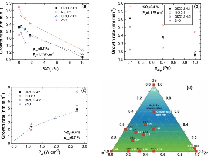
4.2 – Dependence of the growth rate on (a) %O2, (b) pdep, (c) Prf and (d) target composition. ... 83
4.3 – XRD diffractograms of (a) In2O3, (b) ZnO and (c) IZO/GIZO thin films annealed up to 500 °C. Films
deposited on Si/SiO2 substrates under the same conditions, with thickness around 200 nm. The bars show the peak positions and relative intensities for cubic In2O3 (JCPDS 06‐0416) and hexagonal ZnO (JCPDS 36‐1451) in (a, c) and (b), respectively. ... 86
4.4 – SEM images of (a) ZnO and (b) GIZO 2:2:1 surfaces, for thin films annealed at 500 °C. ... 88
4.5 – Topography AFM images of (a) ZnO and (b) GIZO 2:4:2 surfaces, for thin films annealed at 500
°C. ... 89
4.6 – TEM analyses of oxide semiconductor thin films annealed at 500 °C: (a) electron diffraction
pattern of a GIZO 2:2:1 film; (b) electron micrograph of an IZO 4:1 cross section, revealing the
presence of amorphous and crystalline domains. The images on the right side present a
magnification of the crystalline domain (top) and the electron diffraction pattern of the same area
(bottom); (c) cross‐section BFSTEM image of the IZO 4:1 film. ... 90
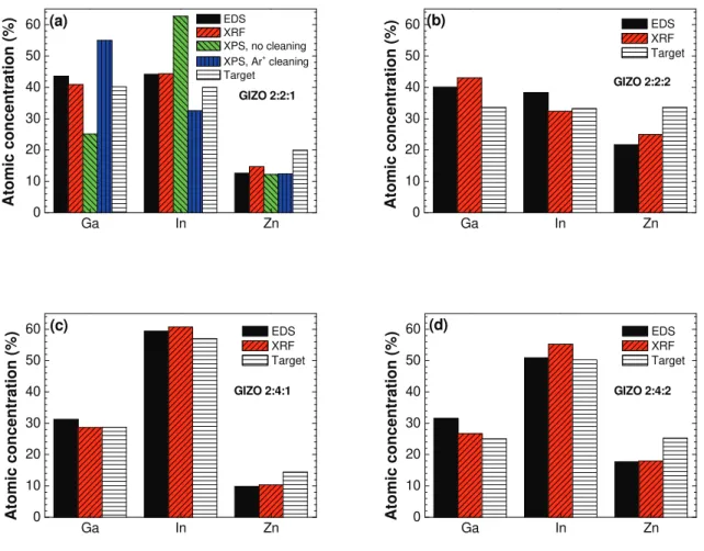
4.7 – Atomic concentrations of gallium, indium and zinc on GIZO thin films produced from targets
with different compositions: (a) GIZO 2:2:1; (b) GIZO 2:2:2; (c) GIZO 2:4:1 and (d) GIZO 2:4:2. The
results were obtained by EDS and XRF for all the compositions and also by XPS for (a), before and
after Ar+ cleaning. ... 91
4.8 – SEM image of the surface of a GIZO 2:2:1 ceramic target. ... 92
4.9 – Atomic concentrations obtained by EDS of gallium, indium and zinc on GIZO thin films produced
from a GIZO 2:4:1 target under different %O2 and Prf, annealed at 500 °C. ... 94
4.10 – Effect of %O2 on ρ for different oxide semiconductors: (a) ZnO; (b) GIZO 2:4:1. Samples
annealed with TA ranging from 150 to 500 °C. ... 95
4.11 – Effect of %O2 on ρ, N and µ for IZO 2:1 thin films annealed at 150 °C. ... 97
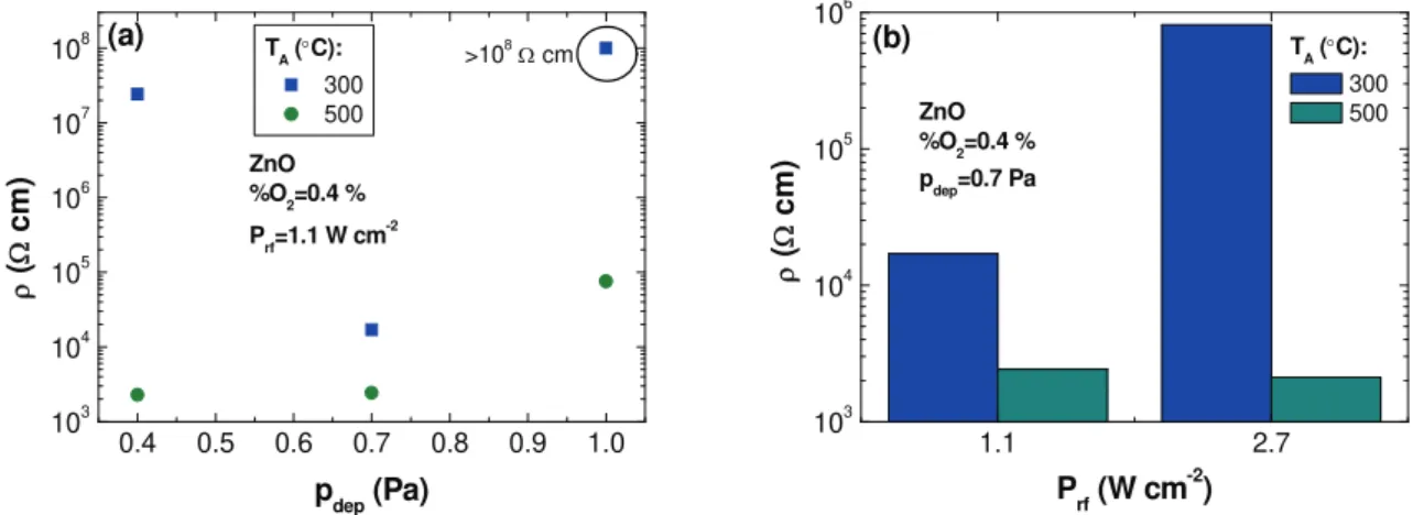
4.12 – Effect of (a) pdep and (b) Prf on ρ for ZnO thin films annealed at 300 and 500 °C. ... 98
4.13 – Effect of (a) pdep and (b) Prf on ρ for GIZO 2:4:1 and IZO 2:1 thin films annealed at TA ranging from 150 to 500 °C. ... 99
4.14 – Effect of target composition on the electrical properties of oxide semiconductor thin films
produced under the same deposition conditions: (a) Effect of In/(In+Zn) and In/(In+Ga) atomic ratios
on ρ, for TA=300 and 500 °C; (b) Ternary diagram for gallium‐indium‐zinc oxide system, showing µ and
N of films annealed at 500 °C. The red and yellow symbols denote amorphous and polycrystalline
4.15 – Effect of TA on N for IZO 2:1 thin films produced with different (a) %O2 and (b) pdep. ... 104
4.16 – Effect of TA on ρ, µ and N for highly conducting IZO 5:1 thin films (for electrode application), produced using the same deposition conditions. ... 106
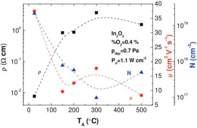
4.17 – Effect of TA on ρ, µ and N for In2O3 thin films produced using the same deposition conditions.
... 107
4.18 – Effect of TA on ρ for In2O3, IZO 4:1 and GIZO 2:4:1 thin films produced using the same
deposition conditions. ... 108
4.19 – Dependence of ρ and µ on N for oxide semiconductor thin films produced under different
deposition conditions, using different target compositions and annealed at 150 and 500 °C. Each
symbol represents a specific target composition. (a) ρ(N), TA=150 °C; (b) ρ(N), TA=500 °C; (c) µ(N),
TA=150 °C; (d) µ(N), TA=500 °C. ... 109
4.20 – Temperature dependence of the electrical properties for ZnO thin films annealed at 500 °C: (a)
Arrhenius plot, showing activation energies for the two suggested regimes; (b) Relation between σ
and T for thermionic emission and VRH conduction mechanisms. ... 113
4.21 – Temperature dependence of the electrical properties for In2O3 thin films annealed at 500 °C:
(a) Arrhenius plot for σ, µ and N; (b) Relation between µ and T using the grain boundary scattering
model for degenerated and non‐degenerated cases; (c) Relation between µ and T using the ionized
impurity and lattice vibration scattering models. ... 114
4.22 – Temperature dependence of the electrical properties (Arrhenius plot for σ, µ and N) for IZO
5:1 thin films annealed at 150 °C, intended to be used as electrodes in TFTs. ... 116
4.23 – Temperature dependence of the electrical properties for GIZO thin films produced with
different compositions, processing conditions and annealed at different temperatures, in order to
assure different N values. Arrhenius plots for (a) σ, (b) µ and (c) N. In (d) the σ data for the GIZO 2:2:2
film is plotted against 1000/T and T‐1/4, to show the possibility of a percolation conduction
mechanism. ... 117
4.24 – ρ measurements in an 18 months time‐scale after the fabrication of the oxide semiconductor
thin films: (a) Effect of %O2 for GIZO 2:4:1 thin films annealed at 150 °C; (b) Effect of composition for thin films annealed at 500 °C. ... 120
4.25 – α‐E plot for a non‐annealed GIZO thin film, showing Tauc and Urbach models fittings to the
experimental data. ... 123
4.27 – Spectroscopic ellipsometry data, showing (a) k‐E and (b) n‐E plots as a function of %O2 for non‐ annealed GIZO 2:4:2 thin films. ... 127
4.28 – α2‐E as a function of (a) In/(In+Zn) and (b) In/(In+Ga) atomic ratios for oxide semiconductor
thin films annealed at 150 °C. Data for the binary oxides (In2O3, ZnO and Ga2O3) is also included for reference. ... 126
4.29 – Spectroscopic ellipsometry data, showing k‐E plots for oxide semiconductor films with
different compositions. Films annealed at 150 °C. ... 127
4.30 – α2‐E plots as a function of TA for (a) In2O3 and (b) ZnO thin films, produced under the same deposition conditions. ... 128
4.31 – Effect of TA on the optical transmittance in the UV‐Visible‐NIR regions for multicomponent oxide semiconductor thin films produced under different processing conditions and compositions, in
order to achieve different N ranges: (a) GIZO 2:4:2 thin films; (b) IZO 5:1 thin films. The insets show
the α2‐
E plots obtained from the transmittance data. ... 129
4.32 – Eopt‐N
2/3 plots for IZO 5:1 and GIZO 2:8:2 thin films, with different
N values obtained by varying
TA. The linear fit shows good agreement of the data with the Burstein‐Moss rule for degenerate
semiconductors. ... 130
4.33 – Spectroscopic ellipsometry data, showing n‐E plots as a function of TA for GIZO 2:8:2 thin films processed using the same deposition conditions. ... 131
4.34 – Process flow used to produce the dielectric thin films. ... 132
4.35 – Growth rates of the sputtered dielectrics. The values inside the bars correspond to the used
Prf. For the co‐sputtered materials (TSiO and TAO), Prf values are given in the form “target #1‐target #2”. ... 132
4.36 – Structural analysis obtained for Ta2O5‐based dielectrics annealed at 300 °C: (a) XRD analysis, where the bars show the peak positions and relative intensities for β crystalline orthorhombic Ta2O5 (ASTM, card 25‐0922); (b) TEM analysis, showing an electron micrograph of a TAO s.t. film cross
section. The inset shows the corresponding electron diffraction pattern. ... 134
4.37 – Compositional analysis obtained by XPS for the Ta2O5‐based dielectric thin films. ... 134
4.38 – Spectroscopic ellipsometry data obtained for the dielectric thin films of (a and b) TSiO and (c
and d) TAO systems. Dependences of n and k on E are presented, for films deposited on c‐Si
substrates. ... 135
4.39 – J‐V characteristics for MIS structures comprising dielectric thin films based on tantalum‐silicon
5.1 – Mask layout used to fabricate the TFTs on commercial Si/SiO2 substrates. ... 148
5.2 – Process flow used to produce TFTs employing commercial Si/SiO2 substrates. The figures in the
bottom show a photograph of a final substrate and a schematic of the device structure. ... 149
5.3 – Effect of %O2 on the electrical properties of GIZO 2:4:2 TFTs annealed at 150 °C: (a) transfer characteristics; (b) Von and On‐Off ratio; (c) µFE and S. ... 151
5.4 – Effect of %O2 on the (a) µFE‐VG evolution and (b) ΔVon after 4 consecutive transfer characteristics measurements. The transfer characteristics as insets in (b) show hysteresis and successive
measurements for %O2=0.4 and 10.0 %, respectively. Results for GIZO 2:4:2 TFTs annealed at 150 °C.
... 153
5.5 – Output characteristics of GIZO 2:4:2 TFTs annealed at 150 °C, for GIZO layers deposited with
different %O2: (a) 0.4 %; (b) 10.0 %. ... 154
5.6 – Effect of (a) pdep and (b) Prf on the transfer characteristics exhibited by GIZO 2:4:2 TFTs annealed at 150 °C. Unless otherwise stated, %O2=0.4 % is used for all the semiconductor layers. The inset in
fig. 5.6b shows the Prf effect for non‐annealed devices. ... 156
5.7 – Effect of oxide semiconductor target composition on the transfer characteristics of TFTs
annealed at 150 °C, with %O2=0.4 %: binary and ternary oxides. ... 159
5.8 – Effect of oxide semiconductor target composition on the transfer characteristics of TFTs
annealed at 150 °C, with %O2=0.4 %: ternary and quaternary oxides. ... 160
5.9 – µFE and Von obtained for TFTs with different oxide semiconductor compositions, in the gallium‐ indium‐zinc oxide system. Devices annealed at 150 °C, with %O2=0.4 %. The red and yellow symbols
denote amorphous and polycrystalline semiconductor films, respectively... 161
5.10 – Transfer characteristics and µFE‐VG plots measured for high VG for TFTs annealed at 150 °C, with %O2=0.4 %, based on (a) GIZO 2:4:2 and (b) ZnO. ... 162
5.11 – Evolution of transfer characteristics of non‐annealed GIZO 2:4:1 TFTs, with %O2=0 %. Devices
stored (a) in vacuum; (b) exposed to air. ... 164
5.12 – Effect of ds on the transfer characteristics exhibited by (a) GIZO 2:8:2 TFTs; (b) GIZO 2:4:2 TFTs. Devices annealed at 150 °C, with %O2=0.4 %. ... 165
5.13 – N and band diagrams for different ds: (a) high; (b) medium; (c) small. ... 167
5.14 – Effect of TA on the transfer characteristics exhibited by TFTs with different semiconductor layers: (a) GIZO 2:2:1, %O2=0.4 %; (b) GIZO 2:4:2, %O2=10.0 %; GIZO 2:8:2, %O2=0.4 %; ZnO, %O2=0.4
5.15 – Electrical properties obtained for the devices depicted in fig. 5.14, having different oxide
semiconductor processes: (a) GIZO 2:2:1, %O2=0.4 %; (b) GIZO 2:4:2, %O2=10.0 %; GIZO 2:8:2,
%O2=0.4 %; ZnO, %O2=0.4 %. ... 171
5.16 – Effect of TA=500 °C on the electrical properties of TFTs: (a) output characteristics of devices
based on GIZO 2:4:1 with %O2=10.0 %; (b) transfer characteristics and µFE‐VG plots for GIZO 2:4:2 TFTs, with %O2=0.4 % and annealing treatments performed before or after source‐drain deposition.
Characteristics of similar TFTs produced on thermal SiO2 are also shown in (b). ... 173
5.17 – Transfer characteristics of 5 similarly processed GIZO 2:4:1 TFTs, with %O2=0 %: (a) non‐
annealed; (b) annealed at 200 °C. ... 175
5.18 – Transfer characteristics of GIZO 2:4:1 TFTs produced with different %O2 on thermal SiO2: (a) non‐annealed; (b) annealed at 300 °C. ... 176
5.19 – Electrical properties of GIZO 2:4:2 TFTs (%O2=0.4 %) produced with Ti/Au and IZO source‐drain
electrodes: (a) Transfer characteristics for TA=150 °C; (b) µFE‐VG plots for TA=150 and 300 °C; (c) Output characteristics of TFTs with Ti/Au electrodes, annealed at 300 °C; (d) Output characteristics of
TFTs with IZO electrodes, annealed at 300 °C. ... 177
5.20 – Band diagrams of different metal‐semiconductor contacts, before (upper) and after (lower)
contact: (a) accumulation; (b) neutral; (c) depletion. [60] ... 178
5.21 – TOF‐SIMS results obtained in Si/SiO2/GIZO/Ti/Au structures (a) before and (b) after 250 °C annealing. ... 180
5.22 – Graphical examples of the main steps involved in the determination of contact resistance and
intrinsic semiconductor parameters by TLM: (a) RT‐L plot for different VG values, allowing to extract
rch and RSD; (b) rch‐ 1‐
VG, allowing to extract VTi and µi. ... 181
5.23 – Width‐normalized 2RSD‐VG and rch.L‐VG plots for different GIZO 2:4:2 TFTs (%O2=0.4 %): (a) devices with Ti/Au and IZO source‐drain electrodes, annealed at 150 °C; (b) devices with Ti/Au
source‐drain electrodes annealed at 150 and 300 °C. Given the low TA in (a), rch.L is assumed to be the same for both Ti/Au and IZO cases. ... 182
5.24 – Width‐normalized 2RSD‐VG and rch.L‐VG plots for TFTs employing a non‐ideal GIZO process (2:2:1, %O2=10.0 %), with Ti/Au source‐drain electrodes and TA=150 °C. ... 183
5.25 – rceff‐VG plots for GIZO 2:4:2 TFTs (%O2=0.4 %) having Ti/Au electrodes, with different ds and TA.
... 184
5.26 – Transfer characteristics of GIZO 2:4:2 TFTs (%O2=0.4 %) annealed at 200 °C prior depositing
°C after passivation layer deposition. In (a), transfer characteristics referring to SiO2 e‐beam and SiO2
sputtering are obtained with VD=1 V. ... 186
5.27 – Transfer characteristics of (a) non‐passivated and (b) SU‐8 passivated GIZO 2:4:2 TFTs, with
%O2=0.4 % and TA=200 °C. Measurements performed in air, under high‐vacuum and after recovering
in air. ... 190
5.28 – (a) µFE‐W/L plot for GIZO 2:4:2 TFTs (%O2=0.4 %) annealed at 150 °C, having W fixed at 50 µm; (b) transfer characteristics of the same devices, with L ranging from 50 to 2 µm. ... 192
5.29 – Results obtained from constant ID stress measurements on GIZO 2:4:2 TFTs annealed at 150 °C, for different %O2: transfer characteristics evolution for (a) %O2=0.4 % and (b) %O2=10.0 %; ΔVT and
ΔS evolution for (c) %O2=0.4 % and (d) %O2=10.0 %. The insets in (c) and (d) show the VG (to assure
ID=10 µA) measured during stress. ... 194
5.30 – Results obtained from constant ID stress measurements on ZnO TFTs with %O2=0.4 % and annealed at 150 °C: (a) transfer characteristics evolution; (b) ΔVT and ΔS evolution. ... 196
5.31 – Summary of the ΔVT and ΔS variations obtained in constant ID stress measurements for TFTs with %O2=0.4 % and annealed at 150 °C (except In2O3, having TA=300 °C), where different target
compositions are used for processing the semiconductor layer: (a) ZnO, In2O3 and IZO; (b) IZO and
GIZO. ... 196
5.32 – Summary of the ΔVT and ΔS variations obtained in constant ID stress measurements for GIZO 2:4:2 TFTs, with %O2=0.4 %, different TA (non‐passivated) and passivated with SU‐8. ... 197
5.33 – Transfer characteristics evolution obtained from constant bias stress measurements on GIZO
TFTs with %O2=0.4 % and annealed at 150 °C, passivated with SU‐8. ... 198
5.34 – Aging effects seen by the evolution of the transfer characteristics of TFTs with different
semiconductor processing conditions and TA: (a) GIZO 2:4:2, %O2=0.4 % and TA=150 °C; (b) IZO 2:1,
%O2=0.4 % and TA=150 °C; (c) GIZO 2:4:1, %O2=10.0 % and TA=150 °C; GIZO 2:4:1, %O2=10.0 % and TA=300 °C. ... 199
5.35 – Mask layout used to fabricate the TFTs on glass substrates with sputtered dielectrics. ... 202
5.36 – Process flow used to produce TFTs on glass substrates employing sputtered dielectrics. In the
bottom is shown a photograph of a final substrate containing 16 TFTs. ... 203
5.37 – Transfer characteristics obtained for GIZO TFTs using different binary dielectrics, annealed at
![Figure 2.3 – Schematic energy‐level diagram for n‐type oxide semiconductors. The arrows at E F represent the E F shift occurring due to intrinsic and/or extrinsic defects. Adapted from [2]](https://thumb-eu.123doks.com/thumbv2/123dok_br/16697324.743875/45.892.347.594.83.331/figure-schematic-semiconductors-represent-occurring-intrinsic-extrinsic-adapted.webp)


![Figure 3.1 – Some of the main effects arising from the interaction between incident ions and the target surface (adapted from [9]). The most important processes of the glow discharge occur close to the target surface, in a region designated by Crookes’](https://thumb-eu.123doks.com/thumbv2/123dok_br/16697324.743875/85.892.319.627.84.328/figure-interaction-incident-important-processes-discharge-designated-crookes.webp)