Raquel Alexandra Antunes Barras
Licenciada em Engenharia de Micro e Nanotecnologias
Cellulose-based composites as functional
conductive materials for printed electronics
Dissertação para obtenção do Grau de Mestre em Engenharia de Micro e Nanotecnologias
Orientador
: Doutor Luís Miguel Nunes Pereira, Professor Auxiliar, Faculdade de
Ciências e Tecnologia da Universidade Nova de Lisboa
Co-orientador
: Bruno Ricardo Quintino Nunes Pereira, Engenheiro, FISIPE
Júri:
Presidente: Professor Doutor Rodrigo Ferrão de Paiva Martins Arguente: Doutora Lídia Sofia Leitão Santos
Vogal: Professor Doutor Luís Miguel Nunes Pereira
Cellulose-based composites as functional conductive
materials for printed electronics
© Raquel Alexandra Antunes Barras
Faculdade de Ciências e Tecnologia
Universidade Nova de Lisboa
Cellulose-based composites as functional conductive materials for
printed electronics i
ACKNOWLEDGMENTS
É com um grande sentimento de satisfação e realização pessoal que entrego este trabalho. Estes ultimos meses foram sem duvida os mais importantes do meu percurso académico e concluir o curso a lembrar-me do primeiro pensamento ao ver a colocação (“entrar foi fácil, sair vamos ver”) é também um grande alivio! Este é o fechar de um ciclo de trabalho que não se fez sozinho e por isso não posso deixar de agradecer a todos os que direta ou indireta fizeram parte dele.
Em primeiro lugar agradeço ao professor Rodrigo Martins e à professora Elvira Fortunato pela oportunidade de trabalhar neste centro de excelência que é o CENIMAT.
Deixo um agradecimento especial ao meu orientador Luís Pereira pela excelente oportunidade oferecida, por toda a orientação, ajuda e ideias, pelas reuniões semanais e almoços que contribuiram muito para a união e motivação de todos enquanto grupo. Este espirito de equipa foi muito importante. Por isto tudo, muito obrigada!
Agradeço ao meu co-orientador o Eng. Bruno Pereira, ao Eng. Paulo Correia e à FISIPE pelo material fornecido pois sem ele realizar este trabalho não teria sido possivel.
Agradeço a toda a equipa do CENIMAT e DCM que se revelaram sempre prestáveis para ajudar em qualquer altura: Alexandra Gonçalves, Rita Branquinho, Tomás Calmeiro, Sónia Pereira, Ana Pimentel, Joana Pinto, Daniela Salgueiro, Cristina Fernades, Carolina Marques, Ana Santa, Pedro Barquinha, Rui Igreja, Carlos Dias, Coro Echeverria, Asal Kiazadeh, Jonas Deuermier, Dona Antónia, Marta Ferreira, António Vicente, Ricardo Ferreira e Tiago Mateus. A estes ultimos, muito obrigada pela máquina de bending! Diana Gaspar, muito obrigada também por toda a ajuda ao longo do trabalho e antes dele, não fosse MCP e não estaria aqui provavelmente.
Um agradecimento especial aos meus amigos e colegas de laboratório, Paul, Tiago, Pedro, Manu e Inês. Melhor grupo não podia ter calhado, foi tão bom ter passado estes meses convosco. Obrigada por toda a ajuda e paciência.
Em especial agradeço à Inês. A tua ajuda foi muito importante. Se no inicio não via isso, agora nada faz mais sentido. Nada se faz sozinho e se duvidas houver estamos cá nós para contar a história. És uma excelente amiga. Um enorme obrigada é pouco pela tua ajuda em tudo, pelos teus planos de trabalho, pelas aulas de inglês (!) e por me teres aturado principalmente.
A todos os meus colegas de curso, para chegar aqui não vim sozinha, a vossa ajuda foi muito importante, por isso agradeço-vos a todos. Em especial à Ana, mais que tudo és a amiga que está sempre lá. Bea, tu também.
Aos meus pais e irmãos Ricardo, Rita e Rafa, vocês são o motivo disto tudo, seja como for. Vêm em ultimo mas são os que importam mais. Obrigada por todo o apoio incondicional. Adoro-vos. Este trabalho dedico-o a vocês.
Cellulose-based composites as functional conductive materials for
Cellulose-based composites as functional conductive materials for
printed electronics iii
ABSTRACT
In this work, cellulose-based electro and ionic conductive composites were developed for application in cellulose based printed electronics. Electroconductive inks were successfully formulated for screen-printing using carbon fibers (CFs) and multi-walled carbon nanotubes (MWCNTs) as conductive functional material and cellulose derivatives working as binder. The formulated inks were used to fabricate conductive flexible and disposable electrodes on paper-based substrates. Interesting results were obtained after 10 printing passes and drying at RT of the ink with 10 % wt. of pristine CFs and 3% wt. of carboxymethyl cellulose (CMC), exhibiting a resistivity of 1.03 Ωcm and a resolution of 400 μm. Also, a resistivity of 0.57 Ωcm was obtained for only one printing pass using an ink based on 0.5 % wt. MWCNTs and 3 % wt. CMC.
It was also demonstrated that ionic conductive cellulose matrix hydrogel can be used in electrolyte-gated transistors (EGTs). The electrolytes revealed a double layer capacitance of 12.10 μFcm-2 and ionic conductivity of 3.56x10⁻⁷ Scm-1. EGTs with a planar configuration, using sputtered GIZO as semiconducting layer, reached an ON/OFF ratio of 3.47x10⁵, a VON of 0.2 V and a charge carrier mobility of 2.32 cm2V-1s-1.
Keywords: carbon fibers, multi-walled carbon nanotubes, cellulose, electric and ionic conduction,
Cellulose-based composites as functional conductive materials for
Cellulose-based composites as functional conductive materials for
printed electronics v
RESUMO
Neste trabalho foram desenvolvidos compósitos celulósicos com condutividade eléctrica e iónica para aplicação em electrónica impressa e baseada em celulose. Foram formuladas com sucesso tintas electrocondutoras para screen printing usando fibras de carbono (CFs) e nanotubos de carbono do tipo multi-walled (MWCNTs) como elementos funcionais para a condução eléctrica e derivados de celulose com a função de espessantes. As tintas formuladas foram usadas para fabricar electrodos condutores flexiveis e descartáveis em substratos derivados de papel. Foram obtidos resultados interessantes após 10 camadas impressas e secas à temperatura ambiente usando uma tinta composta por 10 % wt. de CFs sem tratamento e 3 % wt. de carboximetilcelulose (CMC), com uma resistividade de 1.03 Ωcm e uma resolução de 400 μm. Conseguiu-se ainda uma resistividade de 0.57 Ωcm para apenas uma camada impressa com a tinta de 0.5 % wt. de MWCNTs e 3 % wt. de CMC.
Demonstrou-se ainda a aplicação de matrizes celulósicas de condutores iónicos na forma de hidrogéis em transístores do tipo electrolyte-gated (EGTs). Os electrólitos apresentaram uma capacidade de double layer de 12.10 μFcm-2 e uma condutividade de 3.56x10⁻⁷ Scm-1. Os EGTs, de configuração planar e com uma camada semicondutora de GIZO alcançaram um rácio de corrente ON/OFF de 3.47x10⁵, uma tensão VON de 0.2 V e uma mobilidade de portadores de carga de 2.32cm2V- 1s-1.
Palavras-chave:fibras de carbono; nanotubos de carbono, celulose, condução eléctrica e iónica,
Cellulose-based composites as functional conductive materials for
Cellulose-based composites as functional conductive materials for
printed electronics vii
LIST OF ABBREVIATIONS
3D – Three dimensional a.u. – Arbitrary units AA – Acetic acid AC – Alternate current AgNW – Silver nanowire BNC – Bacterial cellulose C – Capacity
CA – Cellulose acetate
CEMOP – Centro de Excelência de Microelectrónica, Optolectrónica e Processos
CENIMAT | i3N – Centro de investigação de materiais/ Instituto de nanoestruturas, nanomodelação e nanofabricação
CF – Carbon fiber
CMC – Carboxymethyl cellulose CNT – Carbon nanotube CV – Cyclic voltametry
DMF – N2O4/N,N-dimthylformamide DSC – Differential scanning calorimetry EC – Ethyl cellulose
ECT – Electrochromic transistor EDL – Electrical double layer
EDLT – Electrical double layer transistor EGT – Electrolyte gated transistor
EIS – Electrochemical impedance measurement EtOH – Ethanol
FET – Field effect transistor FIB – Focused ion beam
FS2 – Felix Schoeller type 2 paper FS3 – Felix Schoeller type 3 paper
FTIR – Fourier transform infrared spectroscopy FWHM – Full width at half maximum
GIZO – Gallium indium zinc oxide HPC – Hidroxypropil cellulose ITO – Thin-doped indium oxide MCC – Microcrystalline cellulose MW – molecular weight
Mw – Molecular weight
MWCNT – Multi-walled carbon nanotube NCC – Nanocrystalline cellulose NFC – Nanofibrillated cellulose
NMMO – N-methylmorpholine-N-oxide monohydrate NP – Nanoparticle
NW – Nanowire PAN – Polyacrilonitrile
PANI-rGO – Polyaniline reduced graphene oxide PC – Polycarbonate
PEG – Polyethylene glycol PEO – Polyethylene oxide PET – Polyethylene terephtalate PI – Polyimide
PVD – Physical vapor deposition R2R – Roll to roll
RFID – Radio frequency identification tags RH – Relative humidity
RMS – Root mean square RT – Room temperature
Cellulose-based composites as functional conductive materials for
printed electronics viii
TFT – Thin film transistor
TGA – Thermal gravimetric analysis Tol – Toluene
Cellulose-based composites as functional conductive materials for
printed electronics ix
LIST OF SYMBOLS
θ – Angle
λ – Wavelength ρ – Resistivity σ – Conductivity σi – Ionic conductivity ω – Angular frequency Cb – Bulk capacitance
CD – Electrical double layer capacitance d – Thickness
Cellulose-based composites as functional conductive materials for
Cellulose-based composites as functional conductive materials for
printed electronics xi
TABLE OF CONTENTS
ACKNOWLEDGMENTS ... I
ABSTRACT ...III
RESUMO ... V
LIST OF ABBREVIATIONS ... VII
LIST OF SYMBOLS... IX
TABLE OF CONTENTS... XI
LIST OF FIGURES ... XIII
LIST OF TABLES ... XV
1. MOTIVATION AND OBJECTIVES ...1
1.1. Motivation ...1
1.2. Objectives ...2
2. GENERAL INTRODUCTION ...3
2.1. Printed electronics: fundamentals and applications ...3
2.1.1. Screen Printing ...4
2.2. Cellulose ...5
2.2.1. Cellulose composite as functional electroconductive material ...6
2.2.2. Cellulose composite as functional ionic conductive material ...7
3. MATERIALS AND METHODS ...9
3.1. Printable cellulose-based electroconductive composite film for paper electronics ...9
3.1.1. Materials and reagents ...9
3.1.2. Mechanical treatments applied to the carbon fibers ...9
3.1.3. Characterization of carbon fibers and multi-walled carbon nanotubes: structural, morphological and electrical analysis ...9
3.1.4. Inks formulation for screen-printing ...9
3.1.5. Screen-printing of conductive patterns ... 10
3.2. Cellulose-based hydrogels applied as the gate dielectric in electrolyte-gated transistors for printed electronics ... 11
3.2.1. Materials and methods ... 11
3.2.2. Preparation and characterization of cellulose-based hydrogels electrolytes ... 11
3.2.3. Fabrication and characterization of electrolyte-gated transistors ... 11
4. RESULTS AND DISCUSSION ... 13
4.1. Printable cellulose-based electroconductive composite film for paper electronics ... 13
4.1.1. Structural, morphological and electrical characterization of carbon fibers ... 13
4.1.2. Structural and morphological characterization of multi-walled carbon nanotubes ... 15
4.1.3. Surface properties and thermal stability analysis of different paper substrates ... 16
4.1.4. Characterization of formulated screen-printing inks and quality of printed patterns ... 18
4.1.5. Electrical conductivity of printed patterns ... 23
4.1.6. Reliability, flexibility, stress conditions and temperature influence on electrical conductivity of screen printed films ... 27
4.1.7. Application to electric circuits ... 29
Cellulose-based composites as functional conductive materials for
printed electronics xii
4.2.1. Electrochemical impedance spectroscopy characterization of the cellulose based
electrolytes ... 30
4.2.2. Equivalent circuit model ... 30
4.2.3. Application to EGTs ... 32
5. CONCLUSIONS AND FUTURE PERSPECTIVES ... 35
5.1. Final conclusions ... 35
5.2. Future perspectives... 36
6. BIBLIOGRAPHY ... 37
Cellulose-based composites as functional conductive materials for
printed electronics xiii
LIST OF FIGURES
Figure 2.1 –CMOS technology with cellulose paper working as substrate and dielectric of n and p-type FETs[17][41](a); Solar cell on Tetra Pack® substrate deposited by physical vapor deposition (PVD) techniques [12] (b); bio-batery on paper substrate[13] (c); screen printed TFTs on cellulose substrate[Adapted from [42]] (d); Screen printed electrochromic display for gas sensing on cellulose cubstrate [Adapted from [43]] (f). ...4 Figure 2.2 – Scheme of hierarchical and chemical structure of cellulose from vegetal origin (Adapted
from [51]). ...6 Figure 4.1 - Photograph of pristine CFs (a) and respective SEM images (b,c). SEM images of CFs
after milling (d) and 6h of ultrasonication (e). ... 13 Figure 4.2 - Statistical study perfomed on CFs in order to optimize their length size (a) by
ultrasonication (the graph shows the percentage of fibers with lengths lower than 81 µm) (b) and milling (c). ... 14 Figure 4.3 - Structural characterization of CFs (pristine, milled and sonicated) by XRD (a) and
influence of temperature on pristine CFs structure (b). ... 14 Figure 4.4–a) Linear regression of resistance values of several carbon ribbons with different lenghts;
representation of the assembly used to measure resistance from a single carbon ribbon (b) and from two carbon ribbons with a connection point (c)... 15 Figure 4.5 –SEM images(a) and XRD diffractogram of MWCNTs (b). ... 15 Figure 4.6–SEM images top view and cross section of a) regular printing paper, b) paper FS2 and c)
paper FS3. ... 16 Figure 4.7 – Topographic mapping of regular printing paper (a), paper FS2 (b) and paper FS3 (c)
through 3D profilometry on an area of 0.5x0.5 mm2. ... 17 Figure 4.8– Contact angle measured with sessile drop method with a volume of 2 µL of ultrapure water
on regular printing paper (a), FS2 paper (b), FS3 paper (c) and 2 µL of a solution of
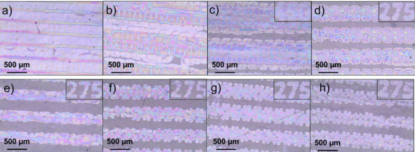
toluene/ethanol (80:20) on FS2 paper (d) and FS3 paper (e). ... 17 Figure 4.9–Thermogravimetric analysis for regular printing paper (a), FS2 (b) and FS3 (c). ... 18 Figure 4.10–Optical micoscope images of the narrower and continuous screen printed lines (on the
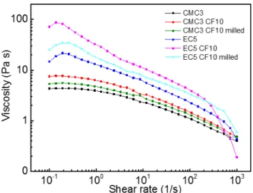
top at the right) obtaind for EC solution with proportions from 2 to 5 %wt (a-d) and CMC solutions proportions from 2 to 5 % wt. (e-h). ... 19 Figure 4.11–Dinamic viscosity of CMC and EC based inks under shear rates from 0.1 to 1000 s-1. .... 21 Figure 4.12 – TGA analysis of CMC3CF10 (a), EC5 CF10 (b), CMC3 CNT0.5 (c) and EC5 CNT0.5 (d) inks. ... 21 Figure 4.13 – FTIR spectra of EC5 (a) and CMC3 (b) solutions measuredt after, 5, 15 30 min after
screen printing. ... 22 Figure 4.14 – Optical microscope images from the narrower and contiunous screen printed lines
obtained from 5 % wt. EC (a) and 3 % wt. CMC (b) based inks with 10 % carbon fibers. ... 23 Figure 4.15 – Optical microscope images of the screen printed films after various printing passes (from
1 to 10), prepared from CMC based electroconductive inks with different concentrations of CFs (1 %, 5 % and 10 % wt.). ... 24 Figure 4.16 – Resisitivity of screen printed patterns of CMC and EC based inks with 10 % wt. as
received carbon fibers with increasing number of printing passes. ... 24 Figure 4.17 - Optical microscope images of the screen printed films after various printing passes (from 1 to 10), prepared from CMC and EC based electroconductive inks of 0.5 % wt. of MWCNTs. .... 25 Figure 4.18 – Resisitivity of screen printed patterns of CMC and EC based inks with 0.5 % of
MWCNTs with increasing number of printing passes. ... 25 Figure 4.19 - Optical microscope images of the screen printed films after various printing passes (from 1 to 10), prepared from CMC and EC and pristine and milled CFs. ... 26 Figure 4.20 – Comparison of electrical performance of CMC and EC based inks prepared with as
received and mechanically treated CFs. ... 26 Figure 4.21–Influence of drying methods on electrical performance of the screen printed filmsfrom
CMC based inks. ... 27 Figure 4.22 – Resisitivity of screen printed films from CMC3 CF10 ink dried at RT. ... 27 Figure 4.23–a) Assembly used to measure temperature inlfuence on electrical resistance of printed
Cellulose-based composites as functional conductive materials for
printed electronics xiv
Figure 4.24 – a) Relative resistance of printed patterns in order to folding angle, here demonstrated using cylinder with several diameters (Measurement conditions: 38% air humidity and 25.6ºC); b) Relative resistance of patterns of 10 screen printed layers of ink CMC3 CF10 after repeated cycles of bending using an automatic machine (Figure 4.23 b) with 5 mm of radius of curvature. (Measurement conditions: 38% air humidity and 25.6ºC). ... 28 Figure 4.25–Evolution of electrical resistance of patterns with10 screen printed layers of ink CMC3
CF10. ... 29 Figure 4.26 –Electric circuit to light a LED fabricated by screen printing using a commercial silver ink
as connectors and the devolped CF aqueous based ink (CMC3 CF10) on the paper FS3 (a). Folding the paper turns the LED ON (b). ... 29 Figure 4.27–A scheme of the parallel plates configuration of electrochemial cell used for EIS
measurements (a) and the equivalen circuit model used for fitting of aquired data (b). ... 30 Figure 4.28 – Data obtained by EIS measurements (red and black circles) and respective fitting with
Randel model (blue line) of MCC4 and MCC8 electrolytes. ... 31 Figure 4.29 – Nyquist plot for MCC4 (a) and MCC8 (b) electrolytes. ... 31 Figure 4.30 – Cyclic voltammogram of both MCC4 and MCC8 electrolytes on the cell performed at
Cellulose-based composites as functional conductive materials for
printed electronics xv
LIST OF TABLES
Table 2.1 – Comparison of some features between several printing technics that can be adapted to printed electronics.[30] ...3 Table 4.1–Thickness measurements of the three types of paper... 16 Table 4.2–Summary of relative advantages of different paper substrates for printed
Cellulose-based composites as functional conductive materials for
Cellulose-based composites as functional conductive materials for
printed electronics 1
1. Motivation and objectives
1.1.
Motivation
Nowadays, there is a growing interest in the area of printed electronics as an alternative to conventional silicon-based electronics. Printed electronics is focused on the development of new low-cost, simple, versatile electronic components and devices through high throughput deposition processes. The implementation of printing techniques on flexible substrates, like plastic foils and cellulose paper, assumes great importance, especially the last when sustainability and recyclability are considered. [1]
Paper is a cheap, ubiquitous, and biofriendly material composed of cellulose fibers that are used as a flexible substrate for many applications in daily life. [2] The strong interest among the scientific and industrial community in the production of electronic or electrochemical devices on cellulose paper substrates is mainly driven by its low cost, lightweight, flexibility and ability to be 100% recyclable. [3] Additionally, cellulose itself is a renewable, biodegradable and the most abundant biopolymer resource available on Earth, with a low environmental impact, being for these reasons considered into a class of materials that may be adapted for the development of innovative electronic composites with new functionalities. [2][4]
Nevertheless, dissolution of cellulose remains a challenge, due to its rigid long-chain and strongly inter-molecular and intra-molecular hydrogen-bonded structure. For this reason, cellulose is usually converted into derivatives, such as sodium carboxymethyl cellulose (CMC) and ethyl cellulose (EC), with interesting properties [5]. Anyhow, several kinds of solvent systems have been developed to prepare new regenerated cellulose [6]. Aqueous alkali hydroxide solutions combined with urea, thiourea, urea/thiourea or PEG have been reported in the literature [7]–[10] as promising solvent systems for cellulose dissolution, due to their simplicity, low cost, low toxicity and rapidity, producing cellulose hydrogels without any hazardous byproducts.
In CENIMAT, paper and electronics have been crossing common paths, with pioneer work being developed on using cellulose paper as substrate for solar cells [11][12], batteries [13], colorimetric sensors [14], and also as gate dielectric in field effect transistors (FETs) [3], [15]–[17]. More recently, the combination of printing techniques with paper as a physical support has been explored for the development of thin film transistors (TFTs) [18], digital microfluidics [19]–[21] electrochromic displays and gas sensors.
Research regarding the exploration of new functional materials based on cellulose became a hot topic. However, not much can be found in the literature about the use of cellulose as an active material in printed electronics, which presents one of the main motivations for the present work.
The hydrophilic nature of cellulose and its ability to form films and hydrogels makes it suitable to act as carrier, matrix or scaffold in new functional materials. Most of the efforts are devoted to the development of composites, where cellulose or its derivatives are combined (through doping, blending or coating) with conductive functional materials, such as carbon structures, conductive polymers, ionic liquids, metal ions and oxides, giving rise to materials with new properties in the form of microspheres, fibers or membranes. [22]
This work aims to bring new insights in cellulose composites. This master thesis is focused on the development and study of cellulose-based composites either as functional electroconductor or ionic conductor materials. The ultimate goal relies in advancing the state-of-the-art in the area of printed electronics, implementing the developed cellulose-based composites.
The use of functional materials, such as electroconductive, based on carbon fibers (CFs) or multi-walled carbon nanotubes (MWCNTs), demands the formulation of suitable inks, which consists in a mixture of the conducting material in a solvent and various additives. Furthermore, it is critical to find the best combination between each component, in order to provide optimal printability combined with high electrical conductivity. Preparation of such inks is challenging, even more when high viscosity is required, as for screen printing, since this condition is only achieved through the addition of polymer binders, like cellulose derivatives (for instance, CMC and EC) that, being non-conducting materials will negatively affect the electrical performance.
Cellulose-based composites as functional conductive materials for
printed electronics 2
successfully used as excellent dispersant of single-walled CNTs (SWCNTs), in terms of stability, high concentration, versatility and film-forming ability. [26]
Taking these considerations into account, cellulose-based electroconductive composite inks were synthesized and formulated with the technical specifications for screen-printing, using a simple and eco-friendly method by blending carbon structures, such as CFs and MWCNTs, into the matrix of a cellulose derivative. EC and CMC were selected as dispersing and stabilizing agents of the carbon structures due to their high viscosity, which enables their use as binders for screen-printing. CFs were selected as conductive functional material thanks to their relatively low cost for industrial scale production (if compared to CNTs) and high availability [27][28]. Nevertheless, CFs are very long (> 100 µm) as compared to CNTs (< 10 µm), which complicates their printability and solution dispersion and stabilization [29]. Thus, mechanical treatments can be a solution in order to reduce their size, but this approach can significantly alter the morphology and aspect ratio of the CFs, reducing the conductivity of the final composite.
The physical properties of the conductive inks and the structure, morphology and electrical properties of the screen-printed films was also focused. These results were correlated with the influence of paper surface properties (such as roughness, porosity and wettability), blending content and morphology of carbon structures, cellulose derivative used as a binder, drying conditions and number of printing passes on print quality and electrical performance of the printed films. The effect of the bending on electrical properties of the screen-printed films was also examined and discussed.
Concerning the development of cellulose-based electrolytes for application in electrolyte-gated transistors (EGTs), not much can be found in the literature regarding EGTs based on cellulose serving as a gate insulator. These devices are able to operate at low voltages, due to the high capacitance achieved by the formation of electric double layers, a very interesting feature for low cost autonomous systems, exactly the type of applications targeted by “printed electronics”. Moreover the EGTs are of particular interest when using printing techniques on substrates that cannot support high temperatures since the electrolyte does not necessarily need any annealing temperature, unlike most solution based dielectric layers.
In this master thesis, we also report the use of cellulose matrix hydrogel electrolytes produced from dissolution of microcrystalline cellulose (MCC) in aqueous LiOH/urea solvent systems as the dielectric layer of EGTs. Here we adapted the conventional procedure, in order to incorporate lithium ions into cellulose, being the resultant cellulose-based hydrogels suitable electrolytes for this specific application.
1.2.
Objectives
The work developed in this master thesis is focused on the development and study of eco-friendly conductive composites based on cellulose, aiming their application as functional layers of printed devices. Two different cellulose composites were designed and engineered based on microcrystalline cellulose (MCC) and cellulose derivatives, such as CMC and EC, which were used as matrix of ionic conductors and electroconductive functional materials based on carbon structures, respectively.
Concerning the development of cellulose-based composites as functional electroconductive material, several studies were performed in order to find the optimal ink composition and screen-printing conditions with the final goal of developing an electroconductive printed pattern. This topic involves the following studies:
Structural, morphological and electrical characterization of the carbon structures;
Physical properties of the formulated inks and their optimization;
Surface properties and thermal stability analysis of different paper substrates;
Optimal conditions for fabrication of screen-printed conductive patterns;
Electrical characterization of the screen-printed conductive patterns;
For the development of cellulose-based composites as ionic conductor materials, this topic will be divided into the following sub-objectives:
Preparation of a cellulose matrix hydrogel electrolyte from MCC, using a simple, fast, low cost and less toxic dissolution method based on aqueous alkali/urea solvent systems;
Electrochemical characterization of the electrolytes;
Cellulose-based composites as functional conductive materials for
printed electronics 3
2. GENERAL INTRODUCTION
For a better understanding of this work, a brief introduction will be given in this section, comprising subjects, such as fundamentals and applications of printed electronics and cellulose. Depending on the functionality, the latter topic is divided into cellulose-based composites either as functional electroconductive materials, incorporating carbon structures such as carbon fibers and multi-walled carbon nanotubes (MWCNTs), or as ionic conductive materials, being some attention given to electrochemical devices, like electrolyte-gated transistors (EGTs).
2.1. Printed electronics: fundamentals and applications
Over the past recent years, research in the area of printed electronics tried to reply to the increasing demand on low-cost, high volume and high-throughput production of lightweight, small, thin, flexible, cheap and disposable electronic components or devices. It’s not a real novelty that most of traditional printing techniques have been adopted for printed electronics. There are reports since before 1950 of using ink solutions and printing techniques to produce circuits on wiring boards. [30] Despite this technology has been surpassed by more accurate deposition techniques back then, the today’s needs on low cost, disposable and flexible technology that cannot be fulfilled by silicon-based electronics are slowly bringing printing electronics back to life. [31]
Fabrication of traditional electronic devices requires the use of vacuum and high temperatures, corrosive chemicals and expensive, sophisticated equipment and infrastructures. Rigid materials, such glass [32] or silicon [33], are often used as substrates because the exposition to such conditions usually are not compatible with the use of flexible substrates, like paper and plastic foils. [34] The possibility of using new deposition methods, such as printing techniques, that don’t require vacuum conditions and can be processed at low temperatures brings great advantages in matter of energy consumption and complexity, opening a new world of low-cost printed circuits based on conductive, semiconductive and dielectric printed materials. [31]
Table 2.1 compares parameters of several printing techniques that can be adapted for printed electronics. For instance, it is possible to obtain a very high definition of patterns using nanoimprint technique, while fast printing speeds are achieved using offset and gravure printing. However, such techniques require complex equipment’s that are more suitable for industrial scale production. Also, inkjet is a simple and cheap technique that allows precise patterning with reduced raw material waste, but the nozzle limits the particles size to very small dimensions (in the order of the dozen of nm) [35]. For a laboratorial scale, screen printing, which will receive further attention in sub-section 1.1.1.,stands out as a promising printing technique, due to its simplicity, adaptability and reliability even when performed manually on an affordable and homemade system.[30]Moreover, screen printing is also scalable to industrial level and compatible with roll-to-roll (R2R) processing.[36] For these reasons, screen printing was selected for development of films with different functionalities, receiving great attention along this work.
Table 2.1 – Comparison of some features between several printing technics that can be adapted to printed electronics.[30]
Viscosity (cp) Line width (µm) Line Thickness (µm) Speed (m/min)
Inkjet 10 – 20 30 - 50 ~ 1 ~ 60
Offset 100 - 10000 ~ 10 < 10 ~ 1000
Gravure 100 - 1000 10 - 50 ~ 1 ~ 1000
Screen 50 - 5000 30 - 50 5 - 100 ~ 500
Nanoimprint - ~ 0,01 ~ 0,1 (Slow)
Cellulose-based composites as functional conductive materials for
printed electronics 4
In particular, paper and cellulose-based substrates have unique characteristics among other flexible substrates, such as the abundance and low cost of cellulose as raw material, associated with its properties of being biodegradable, renewable and recyclable. [34][37] Nevertheless, paper exhibits a porous structure and a large surface roughness, with peak-to-valley roughness values of up to hundreds of micrometers, with a series of shortcomings to hosting electronic devices on its surface associated to its high absorbency. [37][38] Thus, paper is a challenging substrate compared to smooth but more expensive and non-biodegradable plastic sheets. [2][4] Countless devices rely on printed electronic technologies, exploiting the potential of paper as a substrate, such as resistors[34], photovoltaic cells [39], transistors [2][34], radio frequency identification tags (RFIDs) [1], sensors [39] and pharmaceutical applications [40].
Figure 2.1a-e shows some examples of electronic devices developed in CENIMAT, where paper is used as the physical support (Figure 2.1a), substrate for solar cells (Figure 2.1b) [11][12] and batteries (Figure 2.1b) [13]. More recently, paper has been exploited as substrate for printed electronics, developing thin film transistor (TFT) devices (Figure 2.1d) and electrochromic displays for gas sensors (Figure 2.1e).
Figure 2.1 –CMOS technology with cellulose paper working as substrate and dielectric of n and p-type FETs[17][41](a); Solar cell on Tetra Pack® substrate deposited by physical vapor deposition (PVD) techniques [12] (b); bio-batery on paper substrate[13] (c); screen printed TFTs on cellulose substrate[Adapted from [42]] (d);
Screen printed electrochromic display for gas sensing on cellulose cubstrate [Adapted from [43]] (f).
2.1.1. Screen Printing
A simple screen printing system [30], as illustrated in Annex A, consists of a flat support with a patronized screen within frame. The support holds the frame and substrate to be printed and also gives stability to the whole structure; the screen made of polyester fibers or stainless steel mesh with an announced thread diameter and aperture is patronized using a photosensitive resin, which after curing forms permeable and not permeable areas over the mesh fibers. The printing technique consists of spreading an amount of ink through the screen with the help of a squeegee, allowing the ink to pass throw the permeable areas and form the desired pattern in the substrate. Screen printing technique allows the printing of patterns of minimum 10 µm, with thickness ranging from 5 to 100 µm, depending on the mesh size and ink composition. [30][35][44]
The quality of printing patterns relies on a number of parameters related with the screen mesh properties, intrinsic ink characteristics, printing speed and external factors embracing the operator. Although in an automatic screen printing machine these factors are well controlled, the same doesn’t happen for manual screen printing.
In a two dimensional point of view, the thread diameter and aperture dictates the maximum resolution that can be achieved. Since small openings within small distance allows more details to be distinguished, resolution factor in inversely proportional to mesh opening and aperture, and a small mesh is what one looks for when searching for good resolution. The film thickness is also greatly influenced by these parameters.
Cellulose-based composites as functional conductive materials for
printed electronics 5
Active elements: responsible for the functional properties;
Solvent: the vehicle for transport and dispersion of the active element;
Binders (or thickeners): used to adjust rheological properties and after curing or drying time, are responsible for incorporating the active element on the solid matrix;
Additives: used to adjust properties, like wettability or surface tension, and improve particle dispersion and stability in the solvent, or even to improve properties in the printed film like porosity after sintering step.
Additionally, external factors, such as speed of squeegee and applied force to spread the ink, are also considered. The combination on these factors are traduced in a measurable parameter, the shear rate, along whose the viscosity of ink varies.
2.2. Cellulose
Social conscience and economic factors are great concerns for today’s consumers and society in general. The combination of eco-friendly and low cost materials are specially desired qualities in the search for new products and, among a wide range of raw materials, biopolymers seems to satisfy both. [47]
Biopolymers are natural occurring polymers, with its origin on living organisms although they can also be obtained by chemical processes. [47] Starch, cellulose, chitosan, gelatin and chitin are some examples of natural occurring biopolymers, among whose cellulose is the most explored. [47]
Cellulose is a renewable and biodegradable biopolymer and the most abundant on Earth, and can be found in plant cell walls, which is the main source, some sea organisms, fungi and bacteria. It is estimated that per year, the amount of available resources reaches 1011 tons, which falls far short from limits of production (only about 2%). [48] For that fact, this raw material has a great value for industry. It’s biocompatibility, high elastic modulus, thermal stability, nontoxicity and low density makes it suitable for a wide range of applications, from paper and textile, food, pharmaceutical and chemical industry to disposable electronics. [48]
Figure 2.2 shows the organization of the hierarchical structure of cellulose. When extracted from plants, cellulose can be found in cell walls in the form of crystalline microfibrils, along with randomly organized hemicellulose. The cellulose molecule is constituted by D-anydroglucopyranose units, linked by β glycosidic bonds and assembled into groups of cellobiose units. The hydroxyl groups along the polymer chain skeleton forms inter bonds, responsible for the microfibrils of crystalline structure, with lateral dimensions of 5 to 10 nm and several micrometers long.[48][49] In these crystalline regions, according with the molecular orientation, cellulose can form different types of allomorphs. The most commonly form found in nature is cellulose I, where all the molecules have the reducing and non-reducing end in the same direction (parallel), with subalomorphs Iα and Iβ presenting a triclinic and a monoclinic structure, respectively. Cellulose II has antiparallel chains and it’s the more stable form of cellulose. Another less occurring allomorphs are cellulose III and IV, which can be obtained from the previous forms. [47]
Cellulose-based composites as functional conductive materials for
printed electronics 6
Figure 2.2 – Scheme of hierarchical and chemical structure of cellulose from vegetal origin (Adapted from [51]).
The hydrogen bonds responsible for the partial crystalline structure of cellulose, and the dense packaging of these regions difficult dissolution of cellulose, which is not soluble in water neither in common organic solvents. The most common used solvent systems are lithium chloride/dimethyl sulfoxide (LiCl/DMSO) [52], lithium chloride/N,N-dimethylacetamide (LiCl/DMAc) [53], N2O4 /N,N-dimthylformamide (DMF) [53], N-methylmorpholine-N-oxide monohydrate (NMMO) [53] and ionic liquids [53], but they are limited to laboratory scale applications, due to volatility, toxicity and high cost. [10]
Recently, Zhangs’s group [10] developed a simple and rapid method based on inexpensive and less toxic solvent systems for cotton linter dissolution at low temperatures thus producing cellulose hydrogels. This approach consists of dissolution of cellulose in aqueous alkali hydroxide solvents systems, such as NaOH/urea [7][8][9], NaOH/thiourea [8], NaOH/Urea/Thiourea [54] and LiOH/Urea [8][9]. Briefly, cellulose is dissolved at low temperatures (between -5 and -12ºC[8]) in the pre-cooled solvent system, under vigorous stirring, and then regenerated in a coagulation bath (such as, ethanol, acetone, t-butanol and aqueous solutions of 5 % wt. H2SO4 or 5 % wt. H2SO4: 5 % wt. Na2SO4[9]). Finally, the hydrogel of regenerated cellulose is washed with deionized water to remove the residual chemical reagents and dried, obtaining transparent and bendable cellulose films with gas barrier properties. Nevertheless, these systems are not able to dissolve cellulose at room temperature conditions and the precise structure of the dissolution mechanism involved is not fully understood. [54][7][8][9]
Alternatively, the substitution of hydroxyl groups by other functional groups results in derivatives of cellulose that are easily dissolved in ordinary solvents and doesn’t need such complex systems. [48] Some examples are ethyl cellulose (EC), hydroxypropyl cellulose (HPC), methyl cellulose (MC), sodium carboxymethyl cellulose (CMC) and cellulose acetate (CA), with a wide range of applications on food, pharmaceutical and cosmetic industry.[5]
The possibility of dissolution of cellulose compounds and its derivatives, and the incorporation of particles with key properties, led to the creation of functional materials that will be discussed in the next sub-sections.
2.2.1. Cellulose composite as functional electroconductive material
Cellulose-based composites as functional conductive materials for
printed electronics 7
of electroconductive properties with high hydration, swellability and biocompatibility properties inherent of cellulose compounds.[22] In fact, it was found that the dispersing ability of CMC is twenty times higher than commonly used dispersing agents as sodium dodecyl sulphate (SDS), in the case of SWCNTs. [26] There are several methods to combine cellulose with conductive materials by blending, coating or doping with the cellulose fibers, being the electroconductive material dispersed on the surface or within the cellulose matrix.[22]Recent work has been developed involving the preparation of these composites, such as conductive and uniformly connected networks of cellulose nanofibers with CNTs and silver nanowires for transparent paper electronics[55], polyaniline reduced graphene oxide coating the surface of cellulose fibers for flexible supercapacitors[56] and CNTs used as doping agent for electrically conductive cellulose aerogels [57].
Although blending cellulose with conductive materials is currently an extremely attractive and advantageous approach, until now not much information can be found about application of this method in printed electronics. So far, Gao and co-workers [25] formulated a stable pristine graphene ink using cyclohexanone and ethyl cellulose, as solvent and stabilizing agent, respectively, which was used to print highly conductive electrodes (9,24x10³ Scm-1) onto paper and plastic foils by inkjet printing. However, graphene foils are difficult to obtain and to use in large scale. As an alternative, other carbon allotropes, such as carbon fibers (CFs) and carbon nanotubes (CNTs), seem to be very promising to this kind of applications.
CFs can be obtained from industrial processes by carbonization of organic compound under temperatures ranging from 700 to 2700 ºC [58][59]. Regarding the atomic structure of CFs, carbon atoms are arranged unto a honeycomb like two dimensional matrix, with hydrogen bridges bonding the graphitic layers, which can be arranged in several possible configurations.[60][61] Manufacturing process of FISIPE, the company that provided the CFs used in this work, consist on a oxidation step (200-300 ºC) followed by the carbonization (1200-1400 ºC) of polyacrilonitrile (PAN) for the production of high quality CFs, and the surface treatment before the milling process guarantee a good dispensability, making it ideal for application in mixing processes (Annex C). [62]
CNTs can be described as graphene foils wrapped up on a cylindrical like structure and can be obtained by several methods, like electrical arc discharge, laser ablation or chemical vapor deposition. Unlike CFs, large scale production of CNTs is still a common problem for all those synthesis methods [63]. Like CFs, CNTs atomic structure are arranged in a hexagonal form (graphene walls) and there are two distinct types of CNTs, the single-walled CNTs (SWCNTs) and the multi-walled CNTs (MWCNTs), as illustrated on Annex D. The high conductivity of CNTs is related to electrical conduction along a one-dimensional direction that prevents the influence of lattice defects on electrical resistance present on three-dimensional crystals (as CFs). [64]
Comparing CNTs with CFs, CNTs have a higher electrical conductivity, while CFs have a relatively low cost and availability.[27] However, the dispersion of this structures in a stable solution is not trivial since van der walls forces of attraction causes the formation of bundles and cluster (mostly for MWCNTs, because of its higher aspect ratio). [23] The use of cellulose derivatives as dispersants of carbon structures was already demonstrated [25] and from several attempts in order to obtain stable dispersions solutions [24], EC is already being used in the formulation of many functional inks [44][46][86][87]. In recent studies, CMC also revealed some excellent properties in terms of good isolation, stability and film-forming ability, even for high concentrations of SWCNTs. [26] Based on this, EC and CMC reveals great potential for the successful preparation of electroconductive inks with carbon structures as active element.
2.2.2. Cellulose composite as functional ionic conductive material
Ionic conductive compounds, or electrolytes, are composed by dissociated salts in a solution, forming positive ions (cations) and negative ions (anions). Electrolytes are characterized by an high ionic conductivity and a ideally electrical insulation behavior [4], being responsible for ionic exchanges in a countless type of electrochemical devices, such as batteries and fuel cells, electrolytic capacitors, electrochromic devices [65][66] and electrolyte-gated transistors (EGTs) [66].
Cellulose-based composites as functional conductive materials for
printed electronics 8
An example of solid electrolytes based on cellulose is the study reported by Taichi et al. [68] In this work, it was developed a new class of solid polymer electrolytes that comprise poly (ethylene oxide), poly (cyano acrylate), lithium bis(oxalate)borate and robust cellulose nonwoven for high-performance lithium batteries. The developed electrolyte exhibits outstanding properties, such as high mechanical integrity strength as compared to pristine PEO solid polymer electrolyte, fair ionic conductivity (3x10- 4 Scm-1) at 60 ºC, and thermostability (up to 160 ºC). The prepared lithium iron phosphate (LiFePO4)/lithium battery using this electrolyte revealed excellent rate capability and high cycling retention, and allowed for a safe and stable operation up to 160 ºC. However, it is often that these devices encountered poor mechanical strength and low ionic mobility (ionic mobility in solids state is limited).
On the other hand, gels present itself as an advantageous alternative, overcoming the problems of ionic conduction in solid electrolytes and partially solving the technical issues of handling in liquid state electrolytes.[69][3] The ability of cellulose to form hydrogels makes it a very interesting alternative for the development of electrolytes and their application in electrochemical devices. [70]
Hydrogels consists of a three-dimensional polymeric network that are able to retain a lot of water on its structure, being H+ and OH- ions responsible of the ionic conductivity.[71]The conductivity of the hydrogels can be increased by the addition of salts or metal particles.[72] There are some reports related with the development and application of such cellulose hydrogel electrolytes.
Ramos et al. [71] reported the preparation and characterization of cellulose hydrogels as functional electrolytes, which are based on a combination of Laponite, CMC, poly (acrylic acid sodium salt) and lithium perchlorate, aiming their application in electrochromic windows. These electrolytes exhibited an ionic conductivity at room temperature (25 °C) in the range of 6 to 9 × 10⁻⁵ Scm−1. It was
successfully demonstrated their application in NiO-based electrochromic windows, showing a significant transmittance modulation around 45 % at 600 nm.
New approaches have been made taking advantageous of the dissolution methods of cellulose involving ionic liquids. Thiemann et al. (2014) developed for the first time cellulose hydrogel electrolytes for application in FETs. [4] These electrolytes were obtained by drop casting of methylphosphanate ionic liquids onto microcellulose films, followed by annealing at 80 ºC for 3 h to induce gelation. The cellulose ionogels exhibit interesting properties, such as transparency, flexibility, transferability and high capacitance (5-15 µFcm-2), finding applications in flexible electronics as high capacitance gate dielectrics for EGTs on paper.
Because of the high capacitance of ionic compounds (1-10 µFcm-2) even when compared to high k dielectrics by at least one order of magnitude [3][73], electrolytes are successfully used in specific types of field effect transistors (FET): the electrolyte gated transistors (EGTs). The field effect is the driving force of current modulation in FETs that are constituted by a semiconductor between the drain a source electrodes and the dielectric layer sandwiched between the semiconductor and the gate electrode. [66] EGTs are characterized by replacing the traditional gate dielectric, such as Ta2O5 [73], TiO2 [74], HfO2 [75], ZrO [76], of conventional FETs by a high capacitance electrolyte. [66]
Cellulose-based composites as functional conductive materials for
printed electronics 9
3. MATERIALS AND METHODS
3.1. Printable cellulose-based electroconductive composite film for paper electronics
3.1.1. Materials and reagents
CFs and MWCNTs (NC7000) were provided by FISIPE and Nanocyl, respectively. CMC (Mw ~250000) and EC (viscosity 300 cP, 5 % in toluene/ethanol 80:20 (lit.), extent of labeling: 48 % ethoxyl) were purchased from Sigma-Aldrich. Ethanol analytical reagent grade was provided by Fisher Scientific and toluene (≥ 99 %) was purchased from Merck. Deionized water (Millipore) was used.
3.1.2. Mechanical treatments applied to the carbon fibers
CFs were used in three forms: as-received, sonicated and milled. Sonication and manual grinding of CFs were performed in order to reduce fibers length and improve their dispersability and printability. Regarding CFs sonication, an aqueous dispersion of CFs was prepared and ultrasonicated with a cylindrical tip (3 mm end cap diameter) for different times in a UP400S sonicator, using the following parameters: amplitude, 40 %; time on, 2 s; time off, 2 s; time of ultrasonication, 30 min to 6 h. The flask with the aqueous dispersion of CFs was placed in a bath of ice water during sonication, in order to prevent rising of the temperature. Sonicated CFs were dried in a petri dish at 70 ºC until complete evaporation of water.
Milled CFs were obtained by dispersing CFs in an acetone bath, followed by manual grinding in a mortar and drying in a petri dish at 70 ºC until complete evaporation of acetone.
3.1.3. Characterization of carbon fibers and multi-walled carbon nanotubes: structural, morphological and electrical analysis
The morphology of CFs (pristine, milled and sonicated) and MWCNTs was examined by scanning electron microscopy (SEM) using a Carl Zeiss Auriga crossbeam (SEM-FIB) workstation instrument equipped with an Oxford X-ray energy dispersive spectrometer. Samples’ preparation procedure for SEM is given in Annex E. Due to the length size of the CFs (> 80 µm) an optical
microscope (Olympus BX51) equipped with an Olympus DP50 camera and the Cell F View Image System Software was used. The dimensions of CFs and MWCNTs were determined from optical microscope and SEM images, respectively, using ImageJ software.
The structural analysis of the carbon structures was done by X-ray diffraction (XRD) using a PANalyticalX’Pert Pro X-ray diffractometer in Bragg–Brentano geometry, with a monochromatic Cu-Kα radiation source (wavelength 1.5406 Å). XRD measurements were carried out from 10 ° to 65 º (2θ), with a scanning step size of 0.017 °. Also in situ variable temperature XRD measurements were performed from RT until 500 ºC, in order to study thermal stability of pristine CFs.
Electrical characterization of CFs was performed using single ribbon precursors and silver paint as contact and using a multimeter to measure resistance for several ribbon lengths.
3.1.4. Inks formulation for screen-printing
3.1.4.1. Inks formulation
Cellulose-based composites as functional conductive materials for
printed electronics 10
3.1.4.2. Measurement of physical properties of the screen-printing inks
The viscosity of the cellulose/carbon inks was measured on Bohlin Gemini HRnanorheometer, in parallel plates geometry (20 mm diameter and 500 µm gap) for steady-state measurements. Temperature was kept at 25 °C and, before starting the measurements, samples were subjected to a pre-shearing stage, with a pre-shear of 1 s−1 applied for 30 s, followed by an equilibration time of 180 s.
A solvent trap was used in order to avoid evaporation. The steady-state measurements were performed for shear rates up to 1000 s−1.
To investigate their thermal stability, thermal gravimetric analysis (TGA) of cellulose derivatives solutions and prepared inks were performed using a Simultaneous Thermal Analyzer (TGA-DSC - STA 449 F3 Jupiter), from room temperature (RT) to 550 ºC with a heating rate of 5 ºCmin-1, in an aluminum pan, under air atmosphere.
3.1.5. Screen-printing of conductive patterns
3.1.5.1. Surface properties and thermal stability analysis of different paper substrates
Three different types of paper substrates were initially considered in order to print the formulated inks: two distinct photographic papers produced by Felix Schoeller (referred to as paper FS2 and FS3) and commercially available printing paper (300 % from Soporcel).Their surface topography and cross section was analyzed by SEM, and three-dimensional (3D) profilometry of surface was performed with an Ambios XP-Plus 200 Stylus Profilometer and the software data compilation from TrueMap. Contact angle measurements of the solvents used in the inks formulation, such as water and a mixture of toluene:ethanol (80:20 % v/v) on the surface of paper were performed using a Dataphysics OCA-15plus Syste, using a 2 µl liquid drop and at least 3 readings were taken on each sample, for different times. The thermal stability was studied by TGA using the same setup and measurement conditions described in 3.1.4.2.
3.1.5.2. Deposition of conductive patterns
The deposition of cellulose-based conductive composite inks was carried out on paper FS3. Because of the relatively high length of the CFs, a patterned polyester screen mold was designed and ordered in a local polygraphic company (I.C.M. Graf, Portugal) with the following characteristics: mesh model, 77-55; mesh count, 190 mesh/inch; aperture, 81 μm; thread diameter, 55 μm; opening, 30 %; fabric thickness, 88-97 μm. Several samples were prepared in order to understand the influence of the number of printing passes (from 1 to 10) and drying conditions performed between each printing pass on their print quality and electrical performance. Each printed layer was dried either at RT conditions for 15 min or in an oven at 120 ºC for 15 min. The latter one was only applied for the electroconductive printed films based on CMC.
In the case of MWCNTs used as electroconductive material, since the particle dimensions do not impose physical limitations to the mesh dimensions, screen printing was carried out using an additional screen mold with following characteristics: mesh model, 120-34; mesh count, 305 mesh/inch; aperture, 45 μm; thread diameter, 34 μm; opening, 30.5%; fabric thickness, 52-57 μm. In order to study the resistivity thickness dependence, several printing passes were performed (from 1 to 10) and each layer was dried at RT for 15 min.
3.1.5.3. Characterization of conductive patterns
Cellulose-based composites as functional conductive materials for
printed electronics 11
3.2. Cellulose-based hydrogels applied as the gate dielectric in electrolyte-gated
transistors for printed electronics
3.2.1. Materials and methods
All reagents were used without further purification. MCC (powder, 20 μm), LiOH (≥ 98) and acetic acid (≥ 99 %) were purchased from Sigma-Aldrich. Urea (≥ 99.5 %) was purchased from Carl Roth, ethanol analytical reagent grade was provided by Fisher Scientific and toluene (≥ 99%) was purchased from Merck. Deionized water (Millipore) was used.
3.2.2. Preparation and characterization of cellulose-based hydrogels electrolytes
3.1.2.1. Preparation of cellulose-based hydrogels electrolytes
An aqueous solution of LiOH/urea with the optimal mass ratio of 4.6:15 wt%, as reported in the literature [9], was used as solvent system in this study. The solution was then pre-cooled in a freezer at -25 ºC, until complete solidification. The frozen solution was then allowed to thaw at RT and the desired amount of MCC was dispersed in the precooled solvent under vigorous stirring at -8 ºC, until its complete dissolution. Additionally, the mixture was neutralized with acetic acid, in order not to damage other layers existing in the final device, and simultaneously cellulose was regenerated. The solutions were stored in a refrigerator at 3 ºC, until being used. Annex H summarizes the electrolyte solutions prepared and the nomenclature attributed to each one, considering their weight percentage.
Electrolyte membranes were prepared for characterization by slow casting and evaporation of water from 10 g of solution under ambient conditions in polystyrene Petri dishes (5.5 cm diameter). The thickness of the resulting membranes was estimated from the average of five measurements using a Mitutoyo digital micrometer.
3.1.2.2. Characterization of cellulose-based hydrogels electrolytes
Electrochemical characterization of the electrolytes was carried at RT, in a typical capacitor structure by depositing the electrolyte between two stainless steel discs with an active area of 0.994 cm2, using a Gamry Instruments Reference 600 potentiostat. Electrochemical impedance spectroscopy (EIS) measurements were performed at 1 V with a superimposed 5 mV AC voltage in a frequency range of 105 Hz to 0.1 Hz. Cyclic voltammetry (CV) measurements were performed in a potential range between -2 V and 2 V, using different scan rates from 25 to 100 mV/s.
3.2.3. Fabrication and characterization of electrolyte-gated transistors
The EGTs devices were produced by conventional physical vapor deposition (PVD), and cellulose-based electrolytes as the gate dielectric. A planar configuration was adopted, using titanium/gold (Ti/Au) as bottom electrodes (source, drain and gate) deposited on glass (Marienfeld) in a conventional architecture, followed by GIZO working as the active oxide semiconductor.
One initial concern of the fabrication process is the substrate cleaning carried out in an ultrasonic bath for 10 minutes, first in acetone and then in isopropanol, after that, rinsed off in deionized water and dried using nitrogen. Afterwards, Ti/Au electrical contacts (6 and 65 nm thick, respectively) were deposited by e-beam evaporation. Then a 35 nm GIZO (Ga2O3–In2O3–ZnO; 1:2:2 mol %) layer was deposited over the patterned electrical contacts region by radio-frequency (RF) magnetron sputtering, at RT, in an AJA ORION system. The semiconductor channel and the electrical patterns were patterned with shadow masks with a channel width (W) of 950 µm and length (L) of 190 µm (W/L = 5). A schematic representation of the proposed devices and fabrication steps and layers with corresponding thickness is given on Annex I.
Cellulose-based composites as functional conductive materials for
Cellulose-based composites as functional conductive materials for
printed electronics 13
4.
RESULTS AND DISCUSSION
4.1. Printable cellulose-based electroconductive composite film for paper electronics
4.1.1. Structural, morphological and electrical characterization of carbon fibers
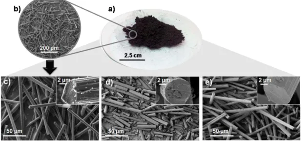
Figure 4.1 a) shows a picture of pristine CFs which exhibit a cylindrical shape with a diameter around 7 µm and a length size around 150 µm, as shown in Figure 4.1b)-c). A high aspect ratio (length/diameter) of the fibers is desirable to improve electrical performance, however CFs with such long length can be a problem for printing. Due to the relatively high length size of the provided CFs, which is slightly bigger than the aperture of the used screen (81 µm) most of the fibers are not able to pass through the screen, affecting the printed pattern and final electrical performance.
In an attempt to reduce their length size, grinding and ultrasonication were performed. Comparing milled (Figure 4.1 d) with sonicated CFs (Figure 4.1 e), it’s clear that the former can significantly alter the morphology of CFs, being severely damage in some cases, reducing the fibers length. On the other hand, sonicated CFs exhibits a morphology very similar to as received pristine CFs. In order to get a better understanding of the influence of each mechanical treatment in the length distribution of CFs, a simple statistical study was carried out by comparing optical microscope images with 200 individual fibers and estimate their length size with ImageJ software.
Figure 4.1 - Photograph of pristine CFs (a) and respective SEM images (b,c). SEM images of CFs after milling (d) and 6h of ultrasonication (e).
As represented in Figure 4.2 a, pristine CFs shows a wide length distribution with an average length size of 123 µm and a standard deviation of 79 µm. More than 60 % of the fibers have a length higher than 81 µm (mesh opening).
For sonicated CFs, samples were collected after 30, 60, 120 and 360 minutes of ultrasonication. In Figure 4.2 is represented the percentage of fibers whose length is higher than 80 µm for different sonication times. For as received pristine CFs, only 45.7 % of the population seem to have a length smaller than 100 µm increasing to 63.4 % after 120 minutes. Longer periods of time seem to not affect significantly this percentage, since that for 360 minutes of sonication, it increases less than 2 %. After milling of the CFs, another sample was observed on optical microscope and again 200 randomly selected fibers were subjected to statistical analysis. In Figure 4.2c), the distribution of the fibers reveals significant differences since 92.5 % seem to have less than 81 µm of length. Thus, milling reveled to be a much more effective treatment than sonication for decreasing fibers length.
Cellulose-based composites as functional conductive materials for
printed electronics 14
Figure 4.2 - Statistical study perfomed on CFs in order to optimize their length size (a) by ultrasonication (the graph shows the percentage of fibers with lengths lower than 81 µm) (b) and milling (c).
The XRD patterns of CFs (pristine, milled and sonicated) are shown in Figure 4.3 a), where the characteristic peaks of hexagonal carbon phase (ICDD File: 00-041-1487) can be identified.[77] All samples reveal one predominant peak at 25.0 º corresponding to (002) plane and two broad peaks less intense around 43.9 º and 51.8 º associated, respectively, to (101) and (004) crystallographic planes.
Regarding in situ XRD measurements performed to pristine CFs under different temperatures from RT to 500 ºC (Figure 4.3b), it is possible to conclude that their structure is not affected, exhibiting thermal stability in this range of temperatures.
Figure 4.3 - Structural characterization of CFs (pristine, milled and sonicated) by XRD (a) and influence of temperature on pristine CFs structure (b).
Cellulose-based composites as functional conductive materials for
printed electronics 15
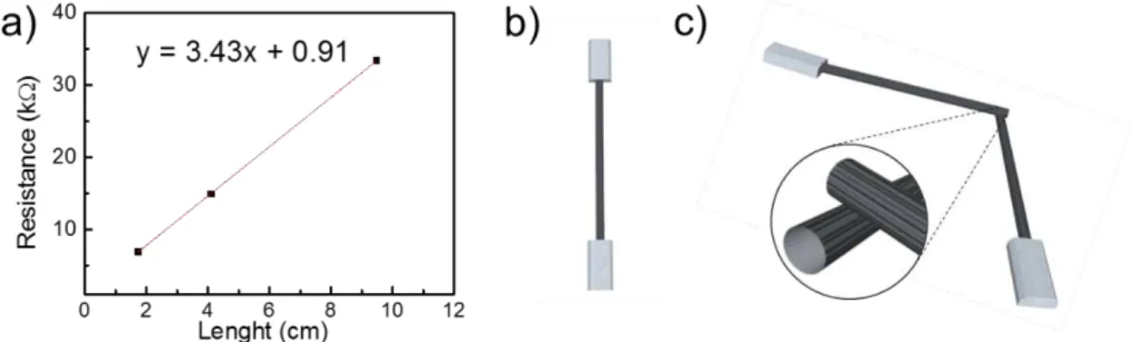
Electrical resistance of an individual carbon ribbon with a length size of 10.4 cm was measured with a multimeter as 35.3 kΩ. Using expression on Annex J and knowing that ribbon diameter is 7 µm, the resistivity was estimated around 1.30x10⁻³ Ωcm. Several measurements of two carbon ribbons connected at some point with a resultant different length was also measured and the linear regression of the collected data is shown in Figure 4.4 a).The slope value (3.43 kΩcm-1) from linear regression represents the resistance per length unit of the ribbons and the correspondent resistivity (1.32 x 10 3 Ωcm), calculated from equation 1, reveals a very similar value for the single fiber with a relative error of 1.54 %. The interception with Y axis is the contribution of contact resistance of the ribbon connection and its value is 0.91 kΩ, which is a significant contribution to the final resistance of the material.
Figure 4.4–a) Linear regression of resistance values of several carbon ribbons with different lenghts; representation of the assembly used to measure resistance from a single carbon ribbon (b) and from two carbon
ribbons with a connection point (c).
4.1.2. Structural and morphological characterization of multi-walled carbon nanotubes Figure 4.5 a) shows SEM images of MWCNTs that were previously dispersed in aqueous solution with a few drops of Triton-X100 and then subjected to ultrasonication for 30 min. This preparation method described in literature [78] was performed in order to improve the dispersion of MWCNTs for SEM imaging, since they are not functionalized and have the tendency to form clusters promoted by Van der Walls attraction [23]. Wherein, it is possible to distinguish individual MWCNTs with length sizes from 1 to 4.3 µm and a diameter of about 15 nm.
XRD analysis of MWCNTs, represented in Figure 4.5 b), shows characteristic peaks at 25.56 º (002), 34.21 º (111) and 43.69 º (101). The XRD pattern of graphite can be used for interpretation with some margin of error since MWCNTs do not present a 3D structure. [79] Wherein, 25.56 º and 43.69 º peak are characteristic of hexagonal graphite (ICDD File: 00-041-1487) and peak at 34.21 º is intended to be associated to some oxidation of the carbon structures (ICDD File: 00-047-1071). The latter peak is related to the presence of CO2 in the atmosphere, during the measurements. However, the analysis of MWCNTs patterns is not straight forward, since their size, curvature and stacking of graphene layers can lead to peak shifts and broadenings. [79]
Cellulose-based composites as functional conductive materials for
printed electronics 16
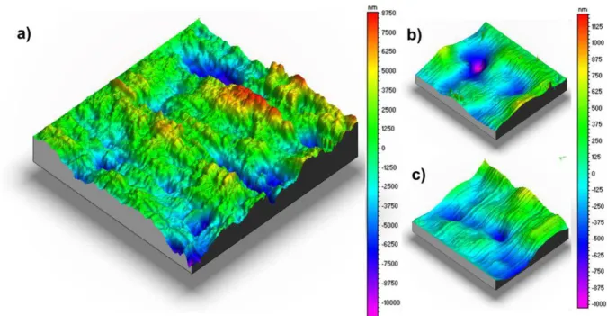
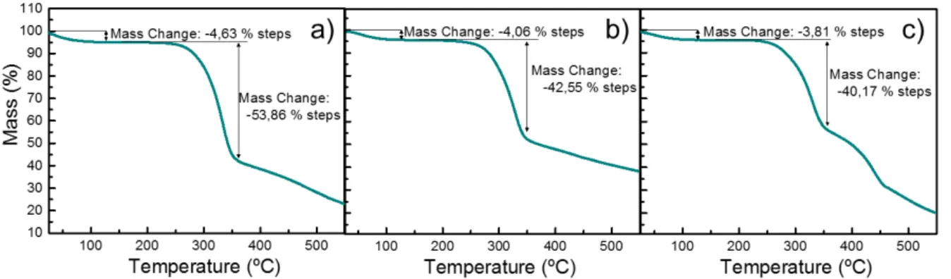
4.1.3. Surface properties and thermal stability analysis of different paper substrates In order to get a functional printed layer with a good printing resolution, there are some concerns related with the ink rheological properties, which must be adapted to each type of substrate used. Wettability and surface morphology are some important parameters that must be considered for selection of a substrate for printed electronics. Furthermore, sometimes is required an additional step of annealing at high temperature for improvement of required properties of the functional printed layer, by removal of solvent trapped in a wet printed layer or elimination of the sacrificial binder. Thus, substrate should be thermodynamically stable under a certain range of temperatures. In this work, three cellulose-based substrates were studied: regular printing paper, paper FS2 and paper FS3.
SEM image of conventional printing paper is shown on a), and its surface reveals a matrix of randomly dispersed long cellulose fibers of about 5 to 15 µm width. Fibers also seem to be flattened, probably due to the compression (calendaring) step during the manufacturing process. Cross section shows packed fibers with a similar structure along paper thickness.
Papers FS2 and FS3 exhibit a much smoother and nanoporous surface as shown on Figure 4.6 b) and c), respectively, contrasting with conventional printing paper. From cross section images it is possible to distinguish different coating layers on the top and bottom side of the raw paper and their respective dimensions. Both papers show one bottom and two top coatings, being the latter responsible for the nanoporous surface. According to the specifications provided by the manufacture, paper FS2 consists of a thick raw paper with a thin backcoating layer, with a pre-coat and nanoporous coating on the top side. For paper FS3, the backcoat and pre-coat are replaced by a resin coating.
The thickness values of each substrate are indicated in Table 4.1. Paper FS2 is thicker than paper FS3, and regular paper is the thinnest from the three substrates.
Figure 4.6–SEM images top view and cross section of a) regular printing paper, b) paper FS2 and c) paper FS3.
Table 4.1–Thickness measurements of the three types of paper.
Regular Paper FS2 FS3
Thickness (μm) 107.40 207.80 180.80
Although through SEM analysis is possible to get some information about surface morphology, 3D scanning profilometry can provide some extra information about the paper surface roughness and quantify it.
![Figure 2.1a-e shows some examples of electronic devices developed in CENIMAT, where paper is used as the physical support (Figure 2.1a), substrate for solar cells (Figure 2.1b) [11][12] and batteries (Figure 2.1b) [13]](https://thumb-eu.123doks.com/thumbv2/123dok_br/16692636.743699/24.892.154.745.385.548/figure-examples-electronic-developed-cenimat-physical-substrate-batteries.webp)
![Figure 2.2 – Scheme of hierarchical and chemical structure of cellulose from vegetal origin (Adapted from [51])](https://thumb-eu.123doks.com/thumbv2/123dok_br/16692636.743699/26.892.205.677.109.438/figure-scheme-hierarchical-chemical-structure-cellulose-vegetal-adapted.webp)