Inuence of Laser Excitation on Raman and
Photoluminescence Spectra and FTIR
Study of Porous Silicon Layers
Walter Jaimes Salcedo
1, Francisco J. Ramirez Fernandez
2, and Joel C. Rubimc
3 1Laboratorio de Espectroscopia Molecular do Instituto de Qumica da USPAv. Prof. Lineu Prestes, 748, 05508-900, S~ao Paulo, SP, Brazil
2Laboratorio de Microeletr^onica, Escola Politecnica,
Universidade de S~ao Paulo, C.P.61548, 05424-970, S~ao Paulo, SP, Brazil
3 Universidade de Brasilia Departamento de Qumica
C.P. 04478, Campus Universitario Asa Norte 70919-970, Braslia-DF
Received February, 1998
A porous silicon lm (PS) was investigated by FTIR, Raman and photoluminescence (PL) spectro-scopies. The Raman and PL spectra were obtained using four dierent laser excitations: 488, 514, 633 and 782 nm. The analysis of the rst order and second order Raman scattering lines permits to identify the band energy structure of the crystallites inside the PS lm. The analysis of PL spectra shows that the intensity and full width at half-maximum values of PL emission depends on intensity and energy of laser excitation. The linear polarization degree (LPD) of the PL spectra also presents a dependence of laser excitation. The observed dependence of Raman and PL spectra due to laser excitation energy cannot be explained within the quantum connement alone. We propose a mechanism for PL emission in PS layers, in which the radiative recombination occurs in localized centers at pore/crystallite interface. These quasi-molecular centers are Jahn-Teller active.
I Introduction
Since the original reports of ecient photoluminescence (PL) from porous silicon (PS) [1,2] the mechanism of the PL from PS is the subject of numerous investiga-tions and discussions [3]. Although experimental ev-idence has been given for the quantum connement model [4], ample arguments and experimental facts have shown that, in silicon nanocrystals with surface passivated by oxide, the PL originates from some ra-diative centers at the nc,Si=SiO
2 interface [5]. One
of the apparently unresolved problems is the large dis-crepancy between the calculated bad gap of the small silicon nanocrystals [6] and the observed distribution of PL spectra [7]. Here we discuss the surface structure, bonding and disorder in PS lms related to PL emission using Fourier Transform Infra Red (FTIR), Raman and PL spectroscopies.
II Experiments and Results
Porous silicon (PS) was prepared by electrochemical an-odization using a Si,p (100) oriented wafer with a
re-sistivity of 10,20 cm. Before anodization, the back
side of wafer was doped with Boron. Ohmic contact was
made by evaporating an aluminum lm. Three samples labeled as A, B and C were prepared. Sample A was prepared by anodization in HF(49%) : H2O(1 : 2),
sample B in HF(49%) : Ethanol(1 : 1) and sample C in HF(49%). Anodization times were of 5, 10 and 30 min with current density of 3, 25 and 40 mA=cm2,
respectively. The thickness of sample A, B and C were of 5m, 5 m and 30 m respectively.
The FTIR spectra of samples were obtained in the BIO-RAD system using transmission technique. The Raman and photoluminescence (PL) spectra were ob-tained on a Renishaw Raman system 3000 equipped with CCD detector and an Olympus BH-2 microscope. Measurements were made in the back scattering geom-etry using a 80microscope objective to focus the laser
beam on the sample. The area of the laser spot on the sample using the 80objective is ca. 2m2m
Figure 1. FTIR and PL spectra in sample A and B.
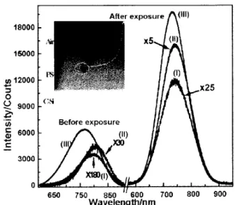
In order to investigate the eect of the laser power density in the PS structure, Raman and PL spectra were obtained before and after exposition of the sam-ples to the maximumlaser power (15 mW at 514:5 nm). To avoid laser damage of the sample before the samples are exposed to the high laser power density, the laser power was set to 50 W. Sample C was cleaved and three micro regions labeled as I, II, and III were ana-lyzed. Region I corresponds to Si/PS interface, Region II to the center of the PS layer, and Region III to the PS/Air interface (see the inset of Fig. 3) . The Raman and PL spectra are shown in Figs. 2 and 3 respectively.
Figure 2. Eect of laser power on the Raman spectra of sample C (cleaved). The spectra were acquired before and after exposure of the dierent regions of the PS layer to 15mW laser power (at 514:5nm). The laser power during spectral acquisition was 50W. The inset shows the curve tting in the 400,600cm
,1spectral region. Regions I, II
and III can be seen in the inset of Fig. 3.
Figure 3. Eect of laser power on the PL spectra of sam-ple C (cleaved). The spectra were acquired before and after exposure of the dierent regions of the PS layer to 15mW
laser power (at 514:5nm). The laser power during spectral acquisition was 50W. The inset shows the white light im-age of sample C indicating the relative position of Regions I, II and III in the sample. The image was obtained with the80 objective.
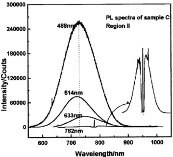
Raman and PL spectra were recorded at 488 nm, 514 nm (from an Ar+ laser), 633 nm (from a HeNe
laser), and 782 nm (from Al=GaAs laser) excitations in order to study the dependence of the phonon and PL spectra on the laser excitation energy . The region II of cleaved sample C was analyzed. The Figs. 4 and 5 show the Raman and PL spectra.
Figure 5. PL spectra of sample C (cleaved) at region II. The spectra were excited with the 488:0, 514:5, 632:8, and 782:0nmlaser radiations.
Polarization measurements of PL spectra were per-formed using an analyzer after the notch lters and a quarter wave plate was set between the analyzer and the entrance slit of the monochromator to correct the grating response for dierent polarization of the scat-tered light. This experimental set-up for polarization measurements was tested with CCl4.
III Discussion
III.1 FTIR spectra
The PS lms A and B were prepared under dier-ent HF concdier-entrations. The FTIR absorption spectra of these samples are quite dierent in the (Si,H
n)
stretching (2100 to 2300 cm,1) and (Si
,O,Si)
stretching (1000 to 1250 cm,1) regions (See Fig. 1).
Sample A (lower HF concentration) shows stronger ab-sorptions in these regions. Note also that the (Si,H
n)
is stronger or sample A. It is worth to mention that the stronger these absorption are, the stronger is the PL emission (See the inset of Fig. 1). Stutzman et. al. [8] have assigned the absorption features at 1080
and 1180 cm,1 to propose that this feature is due to
(Si,O,Si) stretching modes. according to these
authors, the surface of the Si-nanocrystallites by Si6
regular rings containing Si,O,Si bridges, forming
a structure similar to the siloxene. Furthermore, they believe that these structures would be responsible for the PL emission on PS lms. Following the Stutzman
et. al. hypothesis, the enhancement of he PL emission
in PS would be due to the increase of Si6 structures.
Therefore, the higher should be the absorptions in the 1000 to 1200 cm,1 region and their relative intensities
should be remain constant. However, as one observes
from Fig. 1, the relative intensity of the absorptions in this spectral region do not remain constant from sam-ple A to B. In samsam-ple A (higher intensity for the PL emission) the absorptions at 1080 and 1180 cm,1 have
almost the same intensity while for sample B the inten-sity of the feature at 1180 cm,1is almost the half f that
at 1080 cm,1. Deak
et. al. [9] have theoretically
esti-mated vibrational frequencies for dierent Si,O,Si
structures in silicon nanocrystallites. They have ob-tained a frequency value of 1079 cm,1for the Si
,O,Si
structure with vacancies that can be correlated to the absorption feature at 1080 cm,1 in the PS layer. The
feature at 1180 cm,1 can be assigned to nu(Si ,OSi
in the Si,O,Si structure without vacancies in
agree-ment with the observations in th ref [10]. The upper shift of this absorption band is due to the electronega-tive of the neighborhood [10]. According to our results, th feature at 1180 cm,1 is well and directly correlated
to the PL emission, contrary to the hypothesis of Lowe
et. al. that proposed the Si-O-Si structure with
vacan-cies ((Si,O,Si) = 1080 cm
,1, called \not bridge
oxygen hole center" (NBOHC), as the surface structure responsible for PL emission.
III.2 Raman Spectra
The LO phonon Raman peak, in the PS lm of sam-ple C obtained with the 514nm laser source, shows a downshift (510 cm,1
,512 cm
,1) relative to LO Raman
peak of c,Si (520cm
,1). Using the phonon
conne-ment model [12], it was determined that crystallites size in PS lm are in the range of 2:8 nm to 3:2 nm. The best t was obtained considering a spherical shape to crystallites. In addition, it was observed another band in the region of 480 cm,1 that was obtained by
decom-position of band in the region of 400 cm,1to 550 cm,1
(see Fig. 2). Stuzmanet. al. [8] attributed this band
to Si6 structure, this structure have D3d symmetry, so
the band should be polarized. However, in previous work Jaimeset. al. [13] showed that this peak presents
depolarised feature. The 480 cm,1 band is attributed
to interface region structure formed by Si,O,SiR or
Si,SiR where R can be H
nor OH or other radicals.
When the PS structure was exposed to the maximum power of the laser source the region of area exposed showed a dark brown color feature. At this region, the peaks of LO phonon Raman did not change the structure, i.e., the crystallite size calculated before is conserved. However, the peak at 480 cm,1 showed an
increase of intensity and full width at half maximum (FWHM) of the band relative to LO phonon Raman band. This feature is correlated with the PL emission intensity increasing as Fig. 3 shows. With the FTIR technique it was observed that Si,O,Si structure
the surface area of the spot in the sample was esti-mated. The value was approximately 600C when the
laser source was of high intensity. It was reported that Si,H
n bonds are broken at
temperatures above 500 C [14]. In the present case
the experiment was made at room temperature under a relative humidity of 60%. During laser exposure, H desorption is produced from the PS surface. After that the H2O molecule reacts with the PS surface forming
the Si,O,SiH n or Si
,O,SiOH as reported by
[15], so these structures are directly responsible for the 480 cm,1 peak in the Raman spectra.
The second order Raman peak at 630 cm,1 and
960 cm,1did not show changes in the intensity relative
to LO phonon Raman peak showing that these peaks do not depend on the surface structure of PS indicating that these features correspond to Si,Si vibration in
the crystallites. The peak at 630 cm,1 is assigned to
TO(X)+TA(X) contribution and the peak at 960 cm,1
is assigned to 2TO(X), 2TO(W) and 2TO(L) contri-bution as it was suggested in [16]. On the other side, the change of position peaks of PL emission band (see Fig. 3) after laser source exposure (15 mW) can be explained as a result of changing R radical in the struc-ture of Si,O,SiR (eg. H by OH). J. L. Goleet. al.
[17] calculated the band gap of the poliatomicmolecules with structure of SiOSiR showing that changing the R radical provoke a changing in the band gap of molecule. Fig. 4 displays the phonon Raman spectra of sam-ple C at four dierent laser excitations. Note that the LO Raman phonon (at ca. 510 cm,1) does not
de-pend on the energy on the laser excitation, since the observed Raman peaks present no shift within the ex-perimental error (1 cm
,1). Delerue
et. al. [6] have
proposed that the radiative recombination is due to di-rect exciton recombination suggesting that there exists a direct dipole transition in the band structure of the crystallites. However, we were not able to say if there is any resonance for the PS LO Raman phonon since we do not have a internal standard. However, the data displayed in Fig. 4 clearly show that there is a signi-cant change on the intensity of the second order Raman peak at 950 cm,1 relative to the LO Raman phonon of
PS (at 510 cm,1). If we consider the intensity ratio
I950=I510, it is larger at 514:5 and 488:0 nm excitation
as compared to the 632:8 and 782 nm excitations. Us-ing the calculated size of crystallites and the quantum connement model [6], the band gap in the crystallites were estimated to be ca. 2:15 to 2:47 eV . The laser excitations at 488:0 and 514:5 nm correspond to 2:54 and 2:20 eV , respectively. Therefore, the enhancement of the 950 cm,1, relative to the LO phonon can be
ex-plained as an indirect band gap resonance as in c,Si
[18].
III.3 Photoluminescence
The intensity and maximum of the PL emission are
dependent on the laser excitation energy (see Fig. 5). The higher is the laser energy the more intense are the PL emission. This is an indication that the light ab-sorption process within the PS layer is dependent on the energy band structure of the crystallite as reported by Baierle et al. [19]. However, we were able to
ex-cite the PL emission with a laser energy (782 nm) that is very close to the PL maximum, showing that the PL emission of PS layers is not directly depend on the crystallite energy band structure as it was suggested for many researchers [1,6,20].
It is worth to mention that the maximum of PL emission does also depend on the laser excitation en-ergy. This observation can be explained by the het-erogeneous surface chemistry presented by the Si-nanocrystallites. In other words, the majority of emit-ters at 488:0 nm excitation have a chemical compo-sition that is dierent from the majority of emitters at 632:8 nm excitation. According to the above dis-cussion, the PL emission is associated with the pres-ence of Si,O,Si,R structures on the surface of
the nanocrystallites. Therefore, the changes on the PL emission maximumupon laser energy can be accounted by the changes in the chemical nature of R.
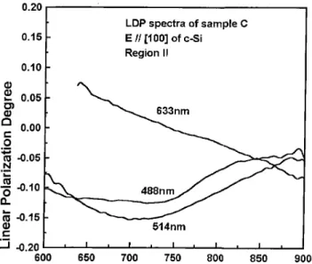
The linear polarization degree (LPD) is dened as (Ik
,I ?)=(I
k+I
?), where I kand I
?represent the
emis-sion band intensity in parallel and perpendicular polar-ization respectively. Fig. 6 shows the spectra of the LPD coecient. At 632:8 nm excitation, the LPD co-ecient shows higher polarization degree at higher en-ergies decreasing slowly for lower emission enen-ergies. On the other hand the LPD coecient shows a dependence on the laser excitation. The LPD values are higher for lower laser energies. Comparing the wavelength of the lasers sources to the crystallite size (2:3 nm to 3:2 nm) one can consider that the electric eld in-side the nanocrystallites is homogeneous and the de-pendence of the LPD coecient on the laser excitation can not be explained as a depolarization eect inside the crystallites.
From the above results based on FTIR, Raman, and PL measurements we can picture the idea that the ra-diative recombination of e,h pairs occurs on localized
centers at the Si nanocrystallite/pore interface in the PS layer. We believe that the Si,O,Si,R structures
radiative recombination at this minimum produces the depolarization of the emission band.
Figure 6. Linear Polarization Degree (LPD) spectra ob-tained by excitation of cleaved sample C at region II. The laser sources were of 488nm, 514nmand 633nm, respec-tively. The incident electric eld was in the [100] direction ofc,Si.
IV Conclusion
Contrary to other infrared studies [8] the results pre-sented here show that PL emission is correlated to Si,O,SiR structures. These structures have
orig-inated localized centers as poliatomic structures. The LO phonon Raman spectra in PS does not show a res-onant behavior. However the second order Raman line at 950 cm,1 presents an indirect band gap resonance
as in c,Si. These results show that the energy band
structure inside crystallites have an indirect band gap as in the c,Si. The Raman line at 480 cm
,1 that is
correlated to PL emission intensity is related to surface structure in the PS lm (Si,OSiR). The PL
emis-sion band intensity of PS layer presents a dependence on laser source excitation indicating the absorption de-pendence on band energy structure inside of crystallite. The LPD coecient shows laser source dependence, in-dicating the localized state as responsible for the ra-diative recombination in PS lm. The FTIR, Raman and PL spectra show that the localized centers are re-sponsible for the radiative recombination in PS lms. The localized centers are formed by poliatomic sys-tem that promotes electron-phonon interactions called Jahn-Teller eects.
Acknowledgements
We acknowledge FAPESP for nancial support.
References
[1] L. T. Canham, Appl. Phys. Lett.57, 1046 (1990).
[2] V. Lehmann and U. Gosele, Appl. Phys. Lett. (1991). [3] M.S. Hybertsen, in: Porous Silicon Technology, eds. J.
C. Vidal and J. Derrien, Springer-Verlag, Berlin 1995, p. 67.
[4] P. D. J. Calcott, N. K. J. Nash, L.T. Canham, M. J. Kane, M. D. Brunhead, J. Phys. C5, L91 (1993).
[5] F. Koch, V. Petrova-Koch and T. Muschik, J. Lumin.
57, 271 (1993).
[6] C. Delerue, M. Lannoo and G. Allan, J. Lumin, 57,
249 (1993).
[7] S. M. Prokes, Appl. Phys.62, 3244 (1993).
[8] M. Stutzmann, Phys. Stat. Sol. (b),192, 273 (1995).
[9] P. Deak, L. C. Snyder and J. W. Corbett; Phys. Rev. B, V.45, 11612, 15 May 1992 - II.
[10] M. Nakamura, Y. Mochizuki, K. Usami; Sol. Stat. Commun., V.50, 1079 (1984).
[11] R. R. Lowe-Webb, H. Lee, J. B. Ewing, S. R. Collins, W. Yang and P. C. Sercel; J. Appl. Phys., V.83, 2815,
1 March 1998.
[12] N. Bruneto, G. Amato; Thin Solid Films, V.297, 122
(1997).
[13] Walter J. Salcedo - Francisco J. R. Fernandez and Joel C. In edition J. Raman Spectroscopy 1999.
[14] H. D. Fuchs, M. Stutzman, M. S. Brandt, M. Rosen-bauer, J. Weber, A. Breitschwerd, P. Deak and M. Car-dona; Phys. Rev. B, V.48, 8172, 15 September 1993-I.
[15] P. Gupta, Surf. Sci. V.245, 360 (1991).
[16] H. Tanino, A. Kupring and H. Deai, Phys. Rev. B.53,
1937 (1996).
[17] J. L. Gole, D. A. Dixon; J. Phys. Chem. B, V.102, 33
(1998).
[18] P. B. Klein, H. Masui, J. Song, R. K. Chang; Solid state Commun, V.14, 1163 (1974).
[19] R. J. Baierle, M. J. Caldas, E. Molinari and S. Ossicini; Sol. Stat. Commun., V.102, 545 (1997).
[20] L. T. Canham; Mat. Res. Soc. Symp. Proc. V.452, 29
(1997).