FACULDADE DE CIÊNCIAS
DEPARTAMENTO DE FÍSICA
Texturization of ZnO:Al thin films and their
application in a-Si:H thin film solar cells
Sílvia da Costa Frias de Barros
Mestrado em Engenharia Física
FACULDADE DE CIÊNCIAS
DEPARTAMENTO DE FÍSICA
Texturization of ZnO:Al thin films and their
application in a-Si:H thin film solar cells
Sílvia da Costa Frias de Barros
Mestrado em Engenharia Física
Dissertação Orientada pelos Professores Doutores:
Aldrin Antony (Universidade de Barcelona)
Maria Margarida Cruz (Universidade de Lisboa)
i
Não estando a exagerar, muitas vezes o trabalho que tornou possível a elaboração desta tese foi duro. Por isso tenho de agradecer a uma mão cheia de pessoas que fizeram com que a aventura de a ir fazer para um país diferente se tornasse numa experiência tão positiva e enriquecedora!
Em primeiro lugar quero agradecer ao professor Aldrin Antony por tão bem ter guiado o meu trabalho e por me ter tornado uma pessoa mais confiante e sem medo. Apesar de o seu método a princípio ter sido difícil, obrigada por toda a compreensão (quando fazia asneiras), dedicação (quando mais precisei) e recompensa (quando cumpria os objectivos) demonstradas, tanto na parte experimental como na parte de escrita.
Quero agradecer à professora Margarida Cruz por toda a atenção que me deu e incansáveis sugestões para melhorar o texto da minha tese, bem como por me ter guiado pelos documentos que foram precisos até à sua entrega.
Ao professor Joan Bertomeu por me ter guiado nos primeiros dias e pela sua disponibilidade.
À Paz digo obrigada por tão bem me ter acolhido no seu gabinete e por me ter ajudado quando o meu castelhano e catalão eram tão maus que quando as pessoas falavam comigo eu respondia sim e ela respondia não (porque a resposta certa era não e eu tinha percebido uma coisa totalmente diferente!). Por me ter mostrado e explicado como tudo funcionava, inclusive como ir de encontro aos ensinamentos do professor Aldrin. Por ter sido uma amiga, me ter dado várias sugestões culturais e me ter levado a conhecer o Razz!
A todo o grupo dos almoços (Paz, Chumi, Paolo, Oriol, José Luís, ...) pelos almoços em sua companhia, pelos jantares para que me convidaram e torneios de mini ping-pong!
À Dora, Pedro e... Sukki! Sem vocês não tinha sido a mesma coisa. Obrigada pelos fabulosos fins-de-semana a conhecer a Catalunya, pelos imensos jantares à meia noite, mojitos e sessões de televisão! Por me terem dado todo o apoio das vezes que fui assaltada e por me terem dado um tecto no último mês! E obrigada ao Sukki por...me ter roubado a roupa! Ainda guardo a meia que ficou desirmanada. Ainda bem que lá estavam, adorei cada momento com vocês.
ii
À Sonja, pelas viagens que vivemos, pelas alegrias e tristezas que partilhámos, por ser a minha companheira de ginásio e de Barcelona e me ter escutado sempre que precisava de desabafar. Por todos os sábios conselhos que me deu e planos que fizemos!
À Esther por ser uma óptima colega de casa e me ter integrado tão bem.
Quero agradecer à Catarina por me ter ido visitar e me ter dado metade da sua cama em Valência, e também à Cat por me ter dado uma cama inteira em Copenhaga!
À Marta pela hospitalidade com que me recebeu em Madrid e me ter obrigado a andar quilómetros apesar de “ser já ali! É ali já ao fundo da rua!”. Da próxima vez tenho de olhar para o mapa e ver que a rua tem mais 3 quilómetros para a frente! Obrigada pela tua visita a Barcelona, passeios e aventuras que tivemos. E tenho também de agradecer seres tão boa ouvinte e uma grande amiga. Obrigada!
A todos os habitantes da residência 40 que, apesar de eu ser uma desnaturada, estão sempre ali para desanuviar a cabeça e ter conversas que me fazem sentir mais quente. Obrigada amigos.
Ao Nuno, por ter estado sempre presente quando mais precisei de apoio. Por me ter ido visitar, ter sido o meu companheiro de viagem pela Europa (sinto falta de passearmos de bicicleta e perdermo-nos e irmos parar a um sítio da cidade que não está no mapa!) e ter tantas vezes sido o meu ombro. Por ter lido várias versões da tese (apesar de não te interessar nada!) e por me ter tirado tantas dúvidas de inglês! Agradeço-te pela tua dedicação, paciência e por me fazeres sentir bem e rir. Como recompensa vou encontrar e oferecer-te um Abacate Sapo!
Por último mas com muito Amor, quero agradecer à minha família... Mãe, Pai e Inês, por me terem proporcionado esta experiência, terem sempre estado a meu lado, dado o apoio que sempre precisei de vocês e serem o meu porto seguro. E obrigada Mãe, pela comida transportável de avião!
iii
As necessidades energéticas da humanidade têm crescido aceleradamente, criando uma forte dependência do mundo civilizado pelas reservas de combustíveis fósseis que se sabe não serem inesgotáveis. Pelo contrário, estas são limitadas e colocam actualmente problemas ecológicos que se prendem com a produção de dióxido de carbono resultante da sua queima, que agravam e aceleram o Aquecimento Global. Este problema implica actualmente a necessidade da procura de fontes de energia alternativa, que sejam renováveis e limpas. Dentro das actualmente viáveis, a energia fotovoltaica, utilizando a radiação solar, é uma das alternativas mais limpas ainda que não suficiente para suprir de imediato as necessidades actuais. Por essa razão tem uma grande importância política, social e económica, todo o desenvolvimento que favoreça uma maior eficiência das células solares. Neste trabalho pretende-se contribuir para esse desenvolvimento, estudando a utilização de filmes texturizados de óxido de zinco dopados com alumínio para janela de entrada da luz, com o objectivo de obter uma maior eficiência de colecção da luz solar e uma melhor conversão fotoeléctrica dessa radiação.
Para esse fim, neste trabalho foram depositados por pulverização catódica assistida por magnetrão sobre substratos de vidro, filmes finos de zinco dopado com alumínio (ZnO:Al) com propriedades adequadas para serem usados como a camada de óxido condutor transparente (TCO) em células solares. O estudo da influência da texturização dos filmes finos de ZnO:Al foi realizado, recorrendo a um processo de texturização e construindo células solares do tipo p-i-n sobre esses filme finos seguindo o processo que se descreve em seguida. Todo o trabalho apresentado foi realizado na Universitade de Barcelona com o Grupo de Energia Solar.
Numa primeira fase, foi desenvolvido e optimizado um processo de limpeza dos substratos de vidro de modo a assegurar que estes se encontravam o mais limpo possível antes da deposição do TCO. Depois de se verificar que o processo de limpeza era adequado, os filmes finos de ZnO:Al foram depositados por pulverização catódica assistida por magnetrão e a texturização foi realizada através de um ataque químico com uma solução de ácido clorídrico (0,5% HCl). As diferentes texturizações obtidas foram morfológica, eléctrica e opticamente analisadas. Alguns dos filmes texturizados foram escolhidos pelas suas características e sobre eles foram fabricadas, pela técnica de deposição química de vapores catalítica por filamento aquecido (HWCVD), células
iv
solares de filmes finos de silício amorfo hidrogenado (a-Si:H), para se estudar a influência da texturização no desempenho dos dispositivos.
Neste trabalho foi desenvolvida a montagem para a texturização e escolhidas as condições de ataque químico definindo algumas variáveis das quais a morfologia resultante depende. Os resultados para a textura são comparados entre si e o comportamento das características medidas das células de a-Si:H depositadas (curva IV, eficiência quântica, factor de preenchimento, tensão em circuito aberto e corrente de curto circuito) é relacionado com a morfologia do TCO. Apresentam-se ainda os resultados obtidos por um programa em MATLAB desenvolvido neste trabalho para se obter uma estimativa do período médio da superfície texturizada e como este valor está relacionado com os parâmetros característicos das células solares.
A estrutura do texto apresentado nesta dissertação é apresentada de seguida. No Prefácio faz-se uma apresentação da importância da energia fotovoltaica e consequentemente do desenvolvimento das células solares tendo em consideração a situação energética mundial. Apresenta-se o tema do trabalho e a estrutura do texto. No capítulo 1 faz-se uma apresentação da constituição e funcionamento das células solares bem como das suas características principais e dos parâmetros mais utilizados para classificar o seu funcionamento. Introduzem-se as diferentes gerações de células solares, as suas vantagens e desvantagens. No capítulo 2 são explicados todos os métodos experimentais aplicados neste trabalho. Dão se os detalhes sobre o processo de limpeza do substrato, desenvolvido e optimizado no quadro desta tese, enunciando-se os protocolos definidos de forma a que o substrato de vidro esteja adequadamente limpo antes da deposição do TCO. Descreve-se o processo de pulverização catódica assistida por magnetrão utilizado para depositar os filmes de ZnO:Al e a montagem utilizada para o processo de texturização. Para estudar o efeito da texturização na qualidade das células solares, utilizou-se a técnica de HWCVD para produzir células solares sobre os diferentes TCO obtidos. Esta técnica é explicada e descrita, bem como o processo de fabrico das células solares. No capítulo 3 são apresentados os resultados da caracterização óptica e eléctrica dos filmes atacados, bem como as suas características morfológicas. Foi ainda realizado o estudo da evolução destas propriedades em função das variáveis do ataque químico. Os resultados são comparados entre si e o comportamento das características medidas das células de a-Si:H depositadas (curva IV, eficiência quântica, factor de preenchimento, tensão em circuito aberto e corrente de
v
resultados obtidos por um programa em MATLAB desenvolvido para se obter uma estimativa do período médio da superfície texturizada e a análise de como estes valores estão relacionados com os parâmetros das células solares. No capítulo 4 são apresentadas as conclusões a tirar dos resultados obtidos e sugeridas propostas para um estudo mais profundo e completo nesta área.
Os resultados principais deste trabalho relacionados com o papel da texturização da camada TCO são os que se descrevem em seguida:
• Com o tratamento químico, a resistência superficial (sheet resistance) de todos os filmes finos de ZnO:Al aumentou, sendo este resultado atribuído à diminuição da sua espessura. Este tratamento químico deve ser realizado numa geometria horizontal para assegurar a homogeneidade da espessura final;
• As condições de pulverização para o crescimento do filme são determinantes no processo de texturização;
• A caracterização óptica dos filmes, medindo a transmissão total e a transmissão difusa e calculando-se a fracção de luz dispersa (“haze”) permitiram concluir que: todos os filmes apresentavam transmitâncias superiores a 83% na banda da luz visível; a transmissão total no infra-vermelho próximo aumenta com o tempo de ataque químico; a transmissão difusa na banda de luz visível aumenta com o ataque químico, atribuído a um aumento da rugosidade da superfície;
• Para as células construídas sobre os filmes de ZnO:Al texturizados, foram analisados os parâmetros seguintes: eficiência quântica externa (EQE), densidade de corrente de curto circuito (Jsc
o A texturização realizada nos filmes ZnO:Al foi transmitida a todas as
camadas da célula;
) e a curva característica (IV), tendo-se concluído que:
o As células depositadas sobre filmes texturizados têm densidades de
corrente de curto-circuito mais elevadas que os filmes não texturizados;
o A melhor eficiência obtida, melhor do que as células construídas sobre
substratos comercialmente disponíveis Asahi-U, foi conseguida numa célula texturizada por ataque químico durante 20s com orientação horizontal;
vi
o Com os filmes ZnO:Al texturizados, obtiveram-se células solares com
eficiências de 3,31% que devem ser comparados com o valor 3,25% obtido nas células depositadas sobre substratos Asahi-U.
Das conclusões retiradas através dos resultados obtidos, são sugeridas algumas propostas para um estudo mais profundo e completo nesta área. As condições de deposição dos filmes finos de ZnO:Al são um parâmetro crítico que determina o resultado da texturização por ataque químico. Neste estudo a melhor escolha de parâmetros incidiu em filmes depositados com uma potência r.f. de 200 W e uma temperatura de 350 ºC para o substrato. Um tratamento mais exaustivo em que sistematicamente se variem estes parâmetros poderá conduzir a filmes cuja texturização resultante seja de melhor qualidade. O tipo e uniformidade da texturização podem também ser melhor caracterizados recorrendo a estudos da distribuição angular da luz dispersa e a imagens de microscopia electrónica de varrimento em secções rectas da superfície.
Palavras-chave: Texturização de filmes finos de ZnO:Al, Texturização TCO, Confinamento Óptico, Células solares de filmes finos de a-Si:H, Deposição química de vapores catalítica por filamento aquecido (HWCVD)
vii
The present work was developed in Barcelona University, with the Solar Energy Group. In this work, ZnO:Al thin films with optimum properties to be used as transparent conductive oxide (TCO) contact layers in solar cells, were deposited by radio-frequency magnetron sputtering onto glass substrates. The main goal of this work was to texturize the as-deposited ZnO:Al thin films for light confinement purposes to achieve an improvement in efficiency of thin film silicon solar cells. The texturization was carried out by wet chemical etching with diluted hydrochloric acid (0,5%HCl), a simple and economic method, with which is possible to improve the light trapping in thin film silicon solar cells. Additionally, amorphous silicon (a-Si:H) thin film solar cells were deposited by HWCVD over the different achieved TCOs, to study the influence of the texturization in the devices performance.
First, a cleaning process was developed and optimized to ensure the glass substrates were very clean prior to deposition of TCO. After checking the cleaning process fulfilled the requisites, the ZnO:Al films were deposited by r.f. magnetron sputtering with optimized process conditions. The texturization set-up was developed, the etching conditions were chosen and the films were etched changing some variables on which the resulting surface morphology depends. The properties of the different resulting textures were morphologically, electrically and optically analyzed. Using the experimental results, some textured films were selected to built a-Si:H solar cells over them. The performance of such solar cells was related with the morphology of the TCO layer. A MATLAB program was developed within the project to find out the average period of the textured surface and how these values are related with the parameters of the solar cells.
The effect of the different textured TCOs in the performance of the deposited a-Si:H solar cells were analyzed and compared. From the conclusions taken are suggested proposals to do a more deep and complete study on this area.
Keywords: ZnO:Al thin films texturization, TCO texturization, Light trapping, a-Si:H thin film solar cells, hot wire CVD
ix
Table of Contents
Preface ... 1
1. Introduction to solar cells and TCOs ... 5
1.1. Solar cells ... 5
1.2. Thin film solar cells ... 6
1.2.1. Si thin film solar cells ... 14
1.3. Transparent Conducting Oxides used in Si thin film solar cells ... 18
1.3.1. ZnO:Al thin films ... 19
1.3.2. Light trapping in Si thin film solar cells ... 20
2. Experimental and Analytical Techniques ... 23
2.1. Substrate Cleaning ... 23
2.2. ZnO:Al deposition by r.f. magnetron sputtering ... 24
2.3. Wet-chemical etching of sputtered ZnO:Al thin films ... 28
2.4. Hot Wire Chemical Vapour Deposition ... 30
2.7. Morphology analysis (AFM and SEM) ... 38
2.8. Solar cell characterization ... 39
3. Results ... 41 3.1. Properties of ZnO:Al ... 41 3.1.1. Electrical properties ... 41 3.1.2. Optical properties ... 44 3.1.2.1. Total transmittance... 44 3.1.2.2. Diffused transmittance ... 46 3.1.2.3. Haze parameter ... 47
3.2. Application of textured ZnO:Al in a-Si:H thin films solar cells ... 48
3.2.1. Electrical characteristics of the solar cell ... 49
3.2.2. Morphology analysis ... 52
4. Conclusions and Remarks ... 63
5. Bibliography ... 67
Appendix A ... 69
xi
List of figures
Figure 1 Share of total primary energy supply in 2006.. ... 1
Figure 1.1 Fermi levels of p and n types. ... 7
Figure 1.2 Fermi levels adjustment ... 7
Figure 1.3 Light effect in a typical I-V curve of a solar cell ... 8
Figure 1.4 Isc and Voc in the I-V curve of a solar cell ... 9
Figure 1.5 I-V curve showing the maximum power point (Vmp, Imp) ... 10
Figure 1.6 Effect of parasitic resistances in I-V curve ... 11
Figure 1.7 Equivalent circuit of a solar cell ... 11
Figure 1.8 Dark I-V curve of a solar cell ... 12
Figure 1.9 Semilog plot of the dark I-V characteristic ... 12
Figure 1.10 External quantum efficiency of a real and an ideal solar cell ... 13
Figure 1.11 Cell technology shares in 2007 ... 14
Figure 1.12 Optical absorption spectrum of µc-Si, a-Si and c-Si ... 15
Figure 1.13 Si thin film solar cell p-i-n and n-i-p-configurations ... 17
Figure 1.14 Typical transmittance spectrum of a magnetron sputtered ZnO:Al film ... 19
Figure 1.15 Solar cell scheme with textured TCO ... 20
Figure 2.1 Scheme of a sputtering system ... 25
Figure 2.2 Aja International sputtering system.... 26
Figure 2.3 Cross section of a sputtering chamber.... 27
Figure 2.4 Schematics of ZnO:Al etching ... 29
Figure 2.5 Water vessels scheme for acid removal. ... 29
Figure 2.6 Schematic representation of the process of HWCVD technique ... 30
Figure 2.7 Overview of the HWCVD used system. ... 32
Figure 2.8 Cross section of a HWCVD deposition chamber. ... 32
Figure 2.9 Used masks for cells deposition and resulting cells format. ... 34
Figure 2.10 a-Si:H cell structure ... 35
Figure 2.11 Four point probe method ... 36
Figure 2.12 Vertical etching with the measurement points ... 36
Figure 2.13 Diffuse light measurement in integrating sphere ... 37
Figure 3.1 Sheet resistance at different points after vertical etching ... 43
Figure 3.2 Sheet resistance at different points after horizontal etching ... 43
xii
Figure 3.4 Total transmittance of the as-deposited flat and etched ZnO:Al thin films ... 45
Figure 3.5 Diffuse transmittances of the etched ZnO:Al thin films ... 46
Figure 3.6 Haze values of the as-deposited flat and etched ZnO:Al thin films ... 47
Figure 3.7 Photograph of solar cells deposited over flat and textured ZnO:Al, and cell scheme ... 48
Figure 3.8 EQE of a-Si:H solar cells fabricated over flat and textured ZnO:Al ... 49
Figure 3.9 EQE of a-Si:H cells deposited over textured ZnO:Al and Asahi-U TCO ... 50
Figure 3.10 I-V curves of cells deposited over textured ZnO:Al and Asahi-U substrates . 52 Figure 3.11 SEM images of ZnO:Al thin films before and after etching ... 53
Figure 3.12 AFM images showing the evolution of the textures with etching ... 54
Figure 3.13 AFM images of the surface texture of a-SiH solar cells ... 54
Figure 3.14 Line profile of the depth measurement of the craters in the textures ... 55
Figure 3.15 Irregularly textured surface of solar cell on ZnO:Al substrate... 55
Figure 3.16 Flow chart of the developed MATLAB program ... 57
Figure 3.17 Image evolution for calculation of average period ... 58
Figure 3.18 Line profile of the textured cell surface deposited over Asahi-U substrates .. 59
Figure 3.19 MATLAB treatment of the image of solar cell ... 59
Figure 3.20 Variation of RMS roughness and haze parameter with average period ... 60
xiii
Table 2.1 Deposition conditions of ZnO:Al sputtered films ... 28
Table 2.2 Etching times for the samples applied in solar cells ... 29
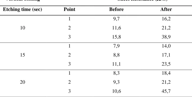
Table 2.3 Deposition conditions of the p, i and n-layers of the HWCVD deposited cells . 33 Table 3.1 Sheet resistance at three points for vertically etched films ... 41
Table 3.2 Sheet resistance at three points for horizontal etched films... 42
Table 3.3 Average sheet resistance of the films applied in solar cells ... 43
Table 3.4 Average % Transmission of the films in the visible range of light ... 43
Table 3.5 Haze values at 600nm of the etched ZnO:Al thin films ... 47
Table 3.6 Short circuit current densities of the a-Si:H solar cells deposited over ZnO:Al and Asahi-U substrates ... 47
Table 3.7 Gain in short circuit current densities of the a-Si:H solar cells deposited over ZnO:Al ... 51
Table 3.8 Characteristics of the a-Si:H solar cells fabricated on different substrates ... 51
Table 3.9 RMS roughness values of the deposited cells ... 55
___________________________________________________________________ 1
Preface
The huge dependence of humanity on fossil fuels and its fast depletion, demand the world to search for alternative and renewable energy sources. The economic, social and political instabilities, limited resources, and war conflicts with countries which have greater fuel reserves lead to the rise of fossil fuel prices. Figure 1 shows the share of total primary energy supply in 2006. Besides the politic and economical problems associated with the use of fossil fuels, they also produce gases that worsen the greenhouse effect leading to Global warming. Because of this, it is crucial to use renewable energy sources like wind, water, geothermal and solar energy, which also have the advantages of being environmental-friendly, virtually unlimited and spread over the entire planet.
Because the global warming’s alarming impacts, the European Union has committed itself to accelerate the reduction of the greenhouse gases (GHG) through the 20- 20-20 programme by 2020 package. The programme aims to reduce carbon dioxide emissions by 20% below 1990 levels, increase to 20% by 2020 the renewable energy share of the total energy mix and improve energy efficiency by 20 percent by 2020.
Figure 1 Share of total primary energy supply in 2006. (Source: IEA)
The solar energy can be effectively utilized using photovoltaic cells. Photovoltaic cells convert directly the incident solar radiation into electricity, by a clean process, the photovoltaic effect, which produces no pollution or harmful wastes, unlike fossil fuels. The average power from the Sun incidenting on the terrestrial surface is around 1000 W/m2 and to satisfy the actual energy consumption, it would be necessary to cover around 0,08% of the earth surface with cells assuming an efficiency of ~10%.
Preface
______________________________________________________________________ 2
In photovoltaic technology, the maximum theoretical efficiency of the single junction solar cell with a 1,5 eV bandgap energy is around 30%. In the case of a solar cell with an infinite number of junctions, the efficiency can be increased up to 60% [13]. This calls for the development of cheaper and efficient solar cells.
The aim of this work is to contribute to the improvement of the efficiency of thin solar cells by increasing the efficiency of light collection in n-i-p structure solar cells based in a transparent layer of aluminum doped zinc oxide (ZnO:Al) thin film. This material has optimum properties to be used as transparent conductive oxide (TCO) contact layer in solar cells, being not as expensive as the traditionally used material. The main goal of the present work was to texturize the as deposited ZnO:Al thin films for light confinement purposes. The texturization was carried out by wet chemical etching with diluted hydrochloric acid (0,5% HCl), a simple and economic method, with which is possible to improve the light trapping in thin film silicon solar cells. Additionally, amorphous silicon (a-Si:H) thin film solar cells were deposited by hot-wire chemical vapor deposition (HWCVD) technique, over the different achieved TCOs, to study the influence of the texturization in the device performance.
This text presents the basics of solar cells and describes the work carried out in detail:
In chapter2, the basic principles of solar cells operation and the difference for the thin film solar cells are introduced as well as the parameters used for their characterization. The two configurations for thin film solar cells are compared and the requirements for materials to be used as TCO are also discussed. The theoretical principles of deposition methods to deposit the TCO and the solar cells and the reasons of their choice are explained. Finally, the principles of light trapping by a textured front TCO are also presented.
In chapter 3 the experimental techniques and procedures followed in this work are explained. After checking the cleaning process, the ZnO:Al films were deposited by r.f.-magnetron sputtering with optimized process conditions. The texturization set-up was developed, the etching conditions were chosen and the films were etched changing some variables on which the resulting surface morphology depends; etching time and substrate orientation. Optical and electrical characterization setups are described. The surface morphology was studied using a scanning electron microscope (SEM) and an
___________________________________________________________________ 3
atomic force microscope (AFM). The HWCVD technique for a-Si:H thin film solar cells deposition is presented.
In chapter 4, the results obtained from the electrical and optical characterization of the etched films, and also their morphological characteristics are presented. The study of the properties as a function of the etching variables was performed. The results are compared and the performance of a-Si:H solar cells (IV-curve, quantum efficiency, fill factor, open circuit voltage, and short circuit current) are related with the morphology of the TCO. Results obtained with a MATLAB program developed to find out the average period of the textured surface, and how these values are related with the parameters of the solar cells are included.
In chapter 5, the conclusions obtained from this work are presented. The proposals for a more deep and complete study on this area is proposed are also suggested.
Preface
______________________________________________________________________ 4
___________________________________________________________________ 5
1. Introduction to solar cells and TCOs
1.1. Solar cells
In 1839, Becquerel discovered the photovoltaic effect, observing that an electric field can be generated between two electrodes attached to a solid or liquid system when illuminated. The modern era of solar cells began in 1954, when the first silicon (Si) solar cell was built at Bell Laboratories, with 6% efficiency.
A simple explanation of the photovoltaic effect is that photons from a source light are absorbed by a semiconducting material and may transfer its energy to the material. The energy is transferred if the energy of the absorbed photon (Eγ) is higher
than the difference in energy levels of the valence and conduction band, the bandgap of the material (Egap). When this happens, an electron is excited to the conduction band
leaving an empty electronic state in the valence band that acts like a positive particle in the semiconductor, which is designated as a hole. Both electron and hole are charge carriers and participate in the electrical transport. Two other possibilities can take place: the photon can be reflected in the material surface or, when Eγ is lower than Egap, the
photon can be transmitted through the material without absorption. The size of Egap
In conductor materials the valence and the conduction band are overlapped, and hence a fraction of the valence electrons can move through the material. Insulator materials are characterized by having large E
determines whether a material is an insulator, a conductor or a semiconductor.
gap values, and therefore electrons do not
move in the material and they do not react to electric fields. A semiconductor has a low enough Egap to allow the thermal excitation of electrons from the valence to the
conduction band and is characterized by an electrical conductivity that varies with the temperature and with external electric fields.
According to the type of construction, solar cells are divided into three generations. The first generation is composed by high quality silicon single junction solar cells with large areas and efficiencies approaching the theoretical limit of 30%. These cells are made from the beginning in high quality volume material, leading to low potential for reducing the production costs [1]. In 2007, 89,6% of the solar cell market was first generation [2].
1. Introduction to solar cells and TCOs
___________________________________________________________________ 6
The second generation had its origin when the solar cell industry began to switch to thin film solar cells, in an attempt to reduce the production costs. The most successful and used materials are cadmium telluride, copper indium gallium selenide and amorphous silicon. These materials are deposited as thin films over a substrate, like glass or ceramics, which reduce the use of mass material and consequently reduce the production costs significantly. These cells have lower efficiencies than the ones of the first generation and in 2007 they were 10,4% of the solar cell market.
The third generation appeared as an effort to enhance the second generation cell efficiency keeping the production costs low, and is still a research target and less successful compared to second generation. The key criterion is the use of new materials, like molecularly based organic and dye sensitized cells [1].
1.2. Thin film solar cells
Thin film solar cells are cells composed of several thin layers of semiconducting materials built on a substrate. The thickness of the layers may vary from a few nanometers to tens of micrometers and thus the thin film classification is done in terms of the production process and not in terms of thickness. A good definition is that a thin film is a material produced from the beginning by the random nucleation and growth process of individually condensing/reacting atomic/ionic/molecular species on a substrate [3]. The electrical, structural and optical properties of the thin films depend on the deposition parameters.
A semiconductor can be doped by introducing impurity atoms into the crystal lattice controlling the concentration of electrons and holes: if the atoms introduced in the crystal lattice have one more valence electron than the original atoms, there will be extra electrons and hence a n-type semiconductor is produced; if the doping atoms have one less valence electron than the ones of the crystal lattice, the semiconductor is p-type, because there are extra holes. The Fermi level of an intrinsic (undoped) semiconductor lies near the middle of the bandgap, but when impurities are introduced it varies. In a n-type semiconductor, the Fermi level lies near the conduction band and in a p-type it lies near the valence band, as presented in figure 1.1 and figure 1.2.
A cell is formed when two different type doped material are placed in contact – p-n junction.
___________________________________________________________________ 7
Figure 1.1 Fermi levels of p and n types.
Figure 1.2 Fermi levels adjustment.
In the contact region, electrons diffuse from the n-side to the p-side and simultaneously holes diffuse from p-side to n-side. This movement results in ionized positive and negative impurities fixed in the crystal lattice on the n-type and p-type sides, respectively, and thus an electric field is created across the junction, in a region with no free carriers. This region is called depletion region and, because of the electric field, the holes tend to stay in p-type semiconductor and electrons in the n-type. It can be said that a diode is created, allowing current to pass easily only in one-way.
If a photon enters the depletion zone with enough energy to excite an electron from the valence to conduction band, a pair electron-hole is formed. Due to the electric field in the depletion zone, electrons are swept to the n-layer and holes to the p-layer, and hence a current is produced. The maximum limit value of this current intensity, in the case of junctions used as solar cells, corresponds to all photons of AM 1.5 spectrum1, with higher energy than the Egap
1
AM - Air Mass is the path length which light takes through the atmosphere normalized to the shortest possible path length (Sun is directly overhead). The light produced by the sun is known as AM0 radiation. AM1.5 radiation corresponds to sunlight that has travel 1,5 times the shortest width of the atmosphere, which occurs when the sun's elevation is 48,2 degrees from the horizontal, a fairly typical value for our latitudes.
for the semiconductor in use, being absorbed, and all electron-hole pairs generated being collected to contribute to the electric current.
1. Introduction to solar cells and TCOs
___________________________________________________________________ 8
The equation of the current generated by one solar cell, I, is similar to the diode equation and is given by equation (1.1), where I0 is the saturation current (the leakage
current density in the absence of light), IL is the light generated current, V is the applied
voltage across the terminals of the diode (cell), q is the absolute value of electron charge, k the Boltzmann's constant, T the temperature of operation of the device and n the ideality factor. I0 is a parameter of the material and depends on Egap.
𝐼𝐼 = 𝐼𝐼0�𝑒𝑒
𝑞𝑞𝑞𝑞
𝑛𝑛𝑛𝑛𝑛𝑛 − 1� − 𝐼𝐼𝐿𝐿 (1.1)
I0 can be determined by the empirical relation, equation (1.2) [3]:
𝐼𝐼0 = 𝐼𝐼00𝑒𝑒−𝐸𝐸𝑔𝑔𝑛𝑛𝑛𝑛 with I00 = 1,5x10⁵ (A. cm−2) (1.2)
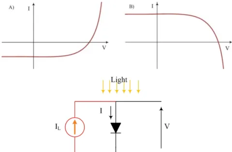
The I-V curve of a solar cell is a combination of the I-V curve of the solar cell diode in dark with the light generated current. When the light shines in the cell, the I-V curve is shifted because power is generated. The greater the light intensity, the greater the power production and so the shift of the curve will be greater. By convention, it is usual to invert the current axis (figure 1.3) in order to have the integral positive for supplied power.
Figure 1.3 Light effect in a typical I-V curve of a solar cell. In figure A) the current axis is not
___________________________________________________________________ 9
The open-circuit voltage (Voc) is the maximum voltage that can be obtained
from the cell when illuminated, and this happens when the current through the device is zero. Voc can be calculated with equation (1.3):
𝑞𝑞𝑂𝑂𝑂𝑂 =𝑛𝑛𝑛𝑛𝑛𝑛𝑞𝑞 𝑙𝑙𝑛𝑛 �𝐼𝐼𝐼𝐼0𝐿𝐿+ 1� (1.3)
The short-circuit current of a cell (Isc) is the maximum current through the cell
and happens when the solar cell is short-circuited, i.e., the voltage across the cell is null (expression (1.4)).
𝐼𝐼𝑠𝑠𝑠𝑠 = −𝐼𝐼𝐿𝐿
(1.4)
An image of the I-V curve with the open-circuit voltage, Voc, and with the
short-circuit current, Isc, is shown below (figure 1.4).
Figure 1.4 Isc and Voc in the I-V curve of a solar cell. (For convention the current axis is inverted).
The fill factor, FF, is related with the form of the I-V curve. It is a parameter that indicates the proximity of the curve to the ideal conditions, and determines the maximum power from a solar cell (figure 1.5). The maximum power of the cell (𝑃𝑃𝑚𝑚𝑚𝑚𝑚𝑚) is given by equation (1.5), and for ideal cells it corresponds to the area of the rectangle in figure 1.4.
1. Introduction to solar cells and TCOs
___________________________________________________________________ 10
So FF is the ratio between the maximum power and the product of Voc by Isc
(equation (1.6)) and for ideal cells FF=1.
𝐹𝐹𝐹𝐹 =𝐼𝐼𝑚𝑚𝑚𝑚 x 𝑞𝑞𝑚𝑚𝑚𝑚
𝑞𝑞𝑜𝑜𝑠𝑠 x 𝐼𝐼𝑠𝑠𝑠𝑠 (1.6)
This corresponds to the ratio of the areas of the shaded rectangles in figure 1.5.
Figure 1.5 I-V curve showing the maximum power point (Vmp, Imp). (For convention the current axis is inverted).
The characteristic resistance of a solar cell is the load resistance at which maximum power is supplied (equation (1.7)).
𝑅𝑅𝑠𝑠ℎ =𝑞𝑞𝑚𝑚𝑚𝑚
𝐼𝐼𝑚𝑚𝑚𝑚 (1.7)
The cell efficiency, η, is obtained dividing Pmax by the incident power, Pinc, and
gives us the fraction of incident power which is converted into electricity (equation (1.8)).
η =Pmax
Pinc (1.8)
This equation can be written as (equation (1.9)):
η(%) =𝑞𝑞𝑜𝑜𝑠𝑠 × 𝐼𝐼𝑠𝑠𝑠𝑠×𝐹𝐹𝐹𝐹
___________________________________________________________________ 11
Parasitic resistances reduce the solar cell efficiency by dissipating power, and the most common are designated as series and shunt resistances. With the I-V curve under illumination it is possible to take information about these resistances because they affect the curve in different regions. In figure 1.6 are represented the referred influences of the resistances.
The series resistance (Rs) is the resistance of the cell material to current flow and
has its cause in the movement of current through the front surface to the contacts and from resistive contacts. This does not affect the open-circuit voltage but strongly affects the I-V curve near it and also reduces the short-circuit current, reducing the fill factor.
Figure 1.6 Effect of parasitic resistances in I-V curve. In image A) is represented the effect of
different values of series resistances (Rs). In image B) is shown the effect of different values of shunt resistances (Rsh
The shunt or parallel resistance (R
).
sh) is typically due manufacturing defects.
Low Rsh
gives rise to leakage current through the cell, because provides an alternate path for the light-generated current, and has no effect in the short-circuit current, but the I-V curve near it is affected and reduces the open-circuit voltage. A typical equivalent circuit of a solar cell is shown in figure 1.7.
1. Introduction to solar cells and TCOs
___________________________________________________________________ 12
The dark I-V curve of a solar cell is the characteristic I-V curve of the cell under no illumination. It is obtained by applying a voltage to the cell, V, i.e., by injecting carriers into the cell instead using the light generated carriers. The I-V characteristic curve essentially corresponds to the curve of a normal diode (figure 1.8), showing that in dark a solar cell is simply a diode.
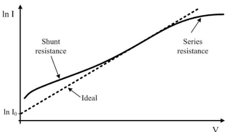
With a semilog graph of the curve, it is possible to extract more information about the diode properties and it also shows how a device operates as a p-n junction and can be used to determine the influence of the shunt and series resistances. It is also possible to calculate the saturation current, 𝐼𝐼0, and have a measure of the recombination rate in the cell: the higher I0, the higher the recombination velocity.
Figure 1.8 Dark I-V curve of a solar cell. The curve corresponds to the curve of a normal diode.
Figure 1.9 Semilog plot of the dark I-V characteristic of an ideal and non ideal solar cell. The series and shunt resistances affect different regions of the curve.
___________________________________________________________________ 13
In figure 1.9 are presented the semilog plot of the dark I-V curves of an ideal cell and of a non-ideal cell. The ideal cell curve is linear, since the I-V curve of an ideal cell is exponential. However, the non-ideal curve shows different regions dominated by different loss mechanisms.
The effect of leakage currents is directed related with low I region of the curve, while the series resistance is related with high current values. The asymptotic current value for zero voltage in the dashed curve gives the saturation current, 𝐼𝐼0.
Another parameter that characterizes a solar cell is the external quantum efficiency, EQE, i.e., the ratio of the number of carriers collected by the solar cell to the number of photons of a given energy incident on the solar cell. This parameter depends on the absorption coefficient of the cell material, the efficiency of charge separation and the efficiency of charge collection.
In figure 1.10 it can be seen the EQE of a real solar cell compared with an ideal one: in zone a) there is a reduction of the EQE due the front surface recombinations in the cell; in zone b) the reduction is due the reflected photons and low diffusion length of the carriers on the cell; zone c) suffers an EQE reduction due rear surface passivation, reduced absorption for long wavelengths and also due low diffusion lengths. The EQE is zero at long wavelengths because no light with energy below the bandgap is absorbed.
Figure 1.10 External quantum efficiency of a real and an ideal solar cell. There is a reduction of
EQE at zones a), b) and c) due different loss processes.
While the optical losses of the device, such as transmission and reflection, are inherent to the external quantum efficiency, the internal quantum efficiency, IQE, refers to photons that are not reflected or transmitted out of the cell, and generate collectable carriers.
1. Introduction to solar cells and TCOs
___________________________________________________________________ 14
1.2.1. Si thin film solar cells
The semiconductors to be used in thin film solar cells should fulfill the following requisites:
• Have a band gap between 1-1,5 eV;
• High solar absorption between 350-1000 nm;
• High quantum yield to the excited carriers;
• Diffusion length of the carriers should be long;
• Low recombination velocity. [3]
Actually the most used semiconductor in solar cells applications (more than 95%) is silicon, Si, due its natural abundance (about 15% of the composition of earth mass) and consequent low cost (figure 1.11). The micro crystalline silicon, µc-Si, has an indirect gap of 1.12 eV, and hence the sunlight is very efficiently absorbed [4]. Because this gap is indirect, to absorb a significant amount of sunlight a film of Si should have a thickness greater than 700 µm [5]. This large thickness implies longer production times and very high production costs. Another disadvantage is that an increased thickness reduces the collection of carriers since the diffusion length of the carriers is in general smaller.
Figure 1.11 Cell technology shares in 2007 (source: EPIA).
Because the absorption coefficient of the Si is low when the energy of the incoming light approaches the Egap of the material, a Si thin film solar cell efficiency is
also low for the corresponding wavelengths and gets worse when the thickness is reduced. One way to enhance the absorption and consequently the efficiency, is to
5,20% 45,20% 42,20% 2,20% 0,50% 4,70% a-Si multi c-Si mono c-Si Ribbon-sheet c-Si CIS CdTe
___________________________________________________________________ 15
increase the optical path length to several times the actual device thickness with a consequent increase of the absorption probability of the photons in the cell (the optical path length of a device refers to the distance that an unabsorbed photon may travel within the device before it escapes out of the device). This can be achieved by trapping the light in the cell, using multireflections within the Si wafer and also by texturizing the transparent conducting oxide (TCO) covering the wafer. The detailed discussion of light trapping is present in Chapter 1.5.1.
The semiconductor used in the solar cells can be amorphous silicon (a-Si), or microcrystalline silicon (µc-Si). The main differences of µc-Si relatively to a-Si are: drastic dependence with the deposition condition and an increased sensitivity to layer contamination; µc-Si has an Egap
• Better absorption under non-direct or weak light conditions;
of 1,1 eV while a-Si has 1,8 eV; this confers to µc-Si a higher absorption in the near infrared region (figure 1.12). Microcrystalline solar cells have efficiencies 9 to 10%, and the best way of using µc-Si is in micromorph tandem cell, which is a combination of a µc-Si cell as a bottom cell with an a-Si solar cell on the top to increase the blue light absorption. This tandem cells efficiency, when stabilized, is between 11%-12% [5]. The most important advantage of a-Si relating to µc-Si in large scale production is its fabrication cost, because a-Si layers can be thinner than µc-Si and hence less material is used. Other advantages are:
• Less sensitive to temperature, so have a better performance under high insulation than µc-Si.
1. Introduction to solar cells and TCOs
______________________________________________________________________ 16
The transparent conducting oxide (TCO) is used as a front contact in thin film solar cells based on amorphous or microcrystalline silicon, and the chosen TCO material must fulfill some requirements for the sake of the good device performance. It acts both as an ohmic contact to transport the carriers out of the device and as a window for light entering the cell. Also, when textured, it has light confinement properties.
1.2.2. p-i-n and n-i-p configurations
An improvement to thin film solar cells is the introduction of an intrinsic layer between p and n regions.
There are two possible configurations for thin film solar cells composed by n, p and intrinsic layers: p-i-n and n-i-p structures (figure 1.13). The great advantage and difference of these configurations to the p-n junction solar cells is the presence of an intrinsic layer. In p-n cells, when the electron-hole pair generation (photon absorption) occurs outside the depletion region, the carriers slowly diffuse towards the depletion region and a significant part of them recombine before reaching it. The ones that reach the depleted area are swept away across the junction to produce an external electrical current. In a p-n junction the depletion region is a small portion of the total device volume and most of the carriers’ generation occurs outside it, implying that the carriers have highly recombined before reaching the depletion region. Also, because of the slow movement towards this region, the current is delayed with respect to photon absorption.
To overcome the recombination problem, the depletion region is increased placing an intrinsic material layer between the p and n doped layers. Because the i-layer has no free carriers, its electrical resistance is high and the potential difference created in p-i and i-n junctions imply strong electrical forces within the i-region that artificially extends the depletion region to a significant fraction of the total solar cell thickness. This means that in these case, most of the photons are absorbed within the depletion region, the generated carriers being immediately swept away by the electric field to the n or p layer, suffering no recombination as in p-n junction case. The higher the i-layer thickness, the higher the probability of photons to be absorbed within it [18]. On the other hand, the field-enhanced collection compensates the short lifetime of the carriers, allowing amorphous silicon to be used in solar cells.
___________________________________________________________________ 17
Figure 1.13 Si thin film solar cell configurations: at the left side is a p-i-n structured solar
cell and in the right side a n-i-p solar cell.
The p-i-n configuration is a superstrate2
• The light enters through the substrate, which is a transparent layer like glass or plastic;
design. The characteristics of this configuration are:
• Because the substrate materials are insulators, it is necessary to deposit a transparent conductive oxide over it;
• The silicon layers are then deposited in p, i and n-layer order over the substrate;
• Finally the back reflector is deposited at the end.
The n-i-p structure is a substrate design and its characteristics are:
• The substrate does not need to be transparent;
• The back reflector is first deposited onto the substrate;
• Then the Si layers are deposited over it in n, i and p-layer order;
• Finally the TCO is deposited behaving as the window for the sunlight to enter into the cell.
So, the main difference between the two configurations is that in the p-i-n structure the sunlight enters by the transparent substrate (a glass or a transparent plastic)
2
1. Introduction to solar cells and TCOs
______________________________________________________________________ 18
and in the n-i-p by the TCO. Typically, the p-layer has a thickness around 20 nm, i-layer a few hundred nanometers and the n-layer around 30 nm.
Because the p-layer is an almost transparent layer, the most part of the photons are absorbed in the thick i-layer. The large i-layer is inside the depletion region and most of the electrons and holes are produced in this region and swept away to the n-layer and p-n-layer [5]. Because the holes are collected in the p-n-layer and have mobilities smaller than the ones of the electrons, the entering of the sunlight is performed through the p-layer.
1.3. Transparent Conducting Oxides used in Si thin film solar cells
A transparent conducting oxide (TCO) material has to be a transparent window (over the spectral region the solar cell is operating) to the cell, to minimize optical losses, and to have low electrical resistance, so the cell series resistance is low. To be transparent, usually a material has to have a bandgap greater than 3 eV so the near UV radiation, around 0.41 µm, can be transmitted to the cell. The material should also have its free carrier plasma resonance absorption in the near-infrared (1.5 µm) or longer wavelengths [7].
The TCO layer has important roles in a solar cell performance: it is a conducting layer over the insulating substrate and, when textured, facilitates the optical confinement. Among the different TCO materials, fluorine doped tin oxide (SnO2
The most usual commercial TCO substrate is the Asahi-U, which consists in a rough layer of tin oxide doped with fluorine, SnO
:F), aluminum doped zinc oxide (ZnO:Al) and indium tin oxide (ITO) are the widely used ones in the Si thin film solar cells. The most used is tin doped indium oxide (ITO), because it is the one that best fits the requirements [7].
2:F, deposited by atmospheric pressure
chemical vapour deposition (APCVD) over a glass. With this technique, films with a rough surface with optical interests are produced, since the roughness of the film is random and has a rms roughness around 35 nm, which is a good value to deposit amorphous silicon solar cells to scatter the light at the front contact [4].
___________________________________________________________________ 19
Recently ZnO thin films have found much application as the front TCO in Si thin film solar cells, since a textured growth of ZnO is possible by metal organic chemical vapour deposition (MOCVD) technique.
1.3.1. ZnO:Al thin films
The high cost and disposability issues of Indium makes necessary to find other TCOs that fulfill the requirements and zinc oxide (ZnO) is one of the alternatives. Although it is not as good as ITO, it is abundant and its costs are lower. Undoped ZnO has a high electrical resistance but it is easy to dope with aluminum (Al), or gallium (Ga) or boron (B) to form good degenerate transparent conducting oxides. ZnO:Al and ZnO:Ga are generally deposited by sputtering technique while the ZnO:B is deposited by MOCVD [12]. One of the advantages of MOCVD grown ZnO is that it will grow with its natural pyramidal texture. This textured ZnO:B can be used as the front transparent contact for the p-i-n type Si thin film solar cells. Other application of doped ZnO thin films in the Si thin film solar cells is in the back reflector stack along with a metallic reflector (Al or Ag).
In figure 1.14 a typical total transmittance spectrum of aluminum doped zinc oxide (ZnO:Al) is represented. Observing the spectrum, it can be noticed that transmittance is zero for 330 nm, which corresponds to a ZnO:Al bandgap energy of ~ 3,8 eV.
1. Introduction to solar cells and TCOs
______________________________________________________________________ 20
1.3.2. Light trapping in Si thin film solar cells
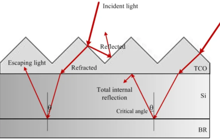
The texturized TCO layer traps light due to the surface topography and also leads to a decrease of reflected light, because a part of the light is reflected back to the cell (see figure 1.15). In this way, it is possible to get an increase in the short circuit current and an increase of the cell efficiency (mainly for long wavelengths, that corresponds to low absorption coefficients and with the increased path length the absorption probability increases).
The Si and ZnO:Al refraction indices are different, the Si index being higher than the ZnO:Al and hence the light is refracted at the interface. An ideal rough surface must have a pyramidal shape so the incoming light can be refracted into angles that are larger than the critical angle for total reflection in silicon. The light is then trapped within the Si absorber layer (figure 1.15). However the pyramids should not be too sharp because the incidence angle in Si would be too small and the light will not be efficiently captured.
Figure 1.15 Solar cell scheme with textured TCO. Light reflected by angles above the critical
angle are totally reflected.
A way to achieve r.f. magnetron sputtered films with surfaces presenting a pyramidal like roughness is to etch them with hydrochloridric acid (HCl). With this technique is possible to give different roughness types, by changing some parameters.
Usually, to characterize a rough surface, the used parameters are: the roughness rms, which is a statistical measurement of the roughness magnitude; the haze, which is
___________________________________________________________________ 21
the ratio between the diffuse and total transmittance and is defined as the portion of light incident on a film that is scattered incoherently; the angular resolved scattering that is a measurement of the scattered light intensity in several solid angles. The different textured ZnO:Al films were used to deposit amorphous silicon thin film solar cells by hot-wire CVD .
1. Introduction to solar cells and TCOs
___________________________________________________________________ 22
___________________________________________________________________ 23
2. Experimental and Analytical Techniques
In this chapter all the processes and steps of the deposition of the ZnO:Al and its chemical wet etching are described, as well the hot wire chemical vapour deposition of amorphous Si thin film solar. All the used set-ups are presented and the optical, electrical and morphological characterization methods are explained.
2.1. Substrate Cleaning
Corning 1737F glass of 5,0 x 5,0 cm2
The initial cleaning process was a simple one, carried out by cleaning the glass with isopropanol (IPA) followed by acetone. Then the process was ended by drying the substrate with blowing nitrogen. After this process, stains on the glass surface were observed, and for this reason a new cleaning process was developed. The applied concepts on the new cleaning process are described below.
area with 1,10 mm of thickness was used as the substrate. The cleaning process of the substrate is a very important step because the thin film growth quality depends on the adhesion and the surface cleanliness, so the substrate must be as clean as possible.
The most important variables in cleaning, using aqueous methods are [14]:
• Precleaning handling; • Cleaner; • Agitation; • Temperature; • Cleaning time; • Rinse used; • Drying method; • Postcleaning handling.
As precleaning condition of the glass substrates, these were stored in protective packages, avoiding them to be exposed to the dusts present in the surrounding atmosphere. The cleaning steps were performed in the Clean Room of Universitat de Barcelona, following the protocol present in Appendix A. Before starting the cleaning
2. Experimental and Analytical Techniques
___________________________________________________________________ 24
processes, the glasses were cleaned with blowing nitrogen, in order to physically remove the dust deposited on the surface.
The cleaning process can be resumed by the following steps:
• Immersion of the substrate in a diluted DECON 90 detergent in deionized water (Millipore Q-POD) in a proportion of 1:4, and manually cleaning with a soft brush. With this, the dust that remained on the surface and the grasses that could be on it were removed;
• Drying with blowing nitrogen and cleaning with DECON 90 detergent in an ultrasonic immersion tank for 5 minutes;
• Rinsing the glass with deionized running water for complete soil and detergent removal;
• Glass drying with blowing nitrogen;
• Cleaning with acetone in the ultrasonic bath for 5 minutes;
• Immersion of the substrate in deionized water immediately after the acetone cleaning, because water is the last thing that should touch the surface [14];
• Finally the water was physically removed by blowing nitrogen over it.
Looking at the substrates with naked eye, it was possible to see that there were no dusts or stains on the surface. After these steps the glasses were stored on clean plastic boxes to prevent dusts to deposit on the surface while transporting to the deposition chamber for the ZnO:Al deposition.
2.2. ZnO:Al deposition by r.f. magnetron sputtering
The ZnO:Al films used in this work were deposited by radio-frequency magnetron sputtering (r.f. magnetron sputtering). This is a Physical Vapour Deposition (PVD) technique used to produce thin films of a wide range of materials, and can be understood as the ejection of material from a source (the target) onto a substrate. The target and the substrate are mounted in a vacuum chamber, facing each other, and there are magnetrons behind the target (thus the name of the technique).
___________________________________________________________________ 25
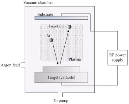
Figure 2.1 Scheme of a sputtering system and some of its components.
The first step to sputter a material is to achieve good vacuum, with a base pressure of typical values from 10-6 to 10-10 Torr. Then a controlled and continuous flow of an inert gas, such as argon (Ar), is introduced in the evacuated chamber until a pressure from 1 to 100 mTorr is established. When power is supplied to the magnetrons and a negative potential is applied to the target (cathode), while the substrate is grounded, a plasma is produced. The plasma is formed due to the ionization of the Ar gas. With the potential difference, the free electrons are accelerated and collide with the gas atoms, ionizing the Ar atoms and producing more electrons to continue the process (figure 2.1). The Ar ions are attracted towards the target surface and collide with it releasing atoms from the target surface. This process is called sputtering. Since these atoms are neutrally charged, they are not affected by the magnetic field and travel to the substrate and collide with it, forming the thin film coating.
When an Ar ion collides with the target surface, the emission of electrons also occurs. The emitted electrons become trapped in the magnetic field produced by the magnetrons, following helical paths around the magnetic field lines contributing to additional collisions between electrons and neutral atoms and the production of more positive ions. These ions are attracted towards the target and the sputtering process is repeated. The trapped electrons form an increased ion density zone near the target implying a high deposition rate and less electrons reaching the substrate. The use of the
2. Experimental and Analytical Techniques
___________________________________________________________________ 26
radio frequency allows the sputtering of insulating materials at a practical rate [8]. Using r.f. the electrodes where the target and the substrate are placed reverse roles on each half cycle. The discharge rate is high enough to avoid charge accumulation in the electrode that is serving as a cathode [9].
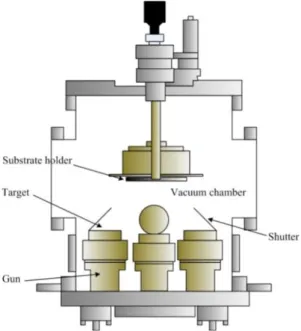
The deposition of the transparent conductive oxide was performed in a commercial sputtering system, ATC ORION Sputtering System of the Aja International Inc. (figure 2.2). The system is equipped three magnetron targets each of capable of holding 3 inch targets. The substrate can be rotated with the rotating feedthrough assembly at 20 rpm and a maximum substrate temperature of 800 ºC can be achieved by radiation heating using halogen lamps. A cross section of the chamber is shown in figure 2.3.
Figure 2.2 Aja International sputtering system.
In this work, a ZnO:Al (ZnO doped with 2 wt% Al2O3
Four 5,0 x 5,0 cm
) sputtering target of 3 inches in diameter and 99,995% purity was used. The distance between the target and the substrate (T-S) can be changed within a range of 11 to 18 cm.The substrate heating is carried out by radiative heating from halogen lamps.
2
glass substrates were used for the deposition at a time, making a square of total area 10 x 10 cm2. The deposition of ZnO:Al was carried out with a substrate rotation of 10 rpm to achieve a better homogeneity.
___________________________________________________________________ 27
Figure 2.3 Cross section of a sputtering chamber.
The shutter position (open/closed) determines whether the deposition begins/ends: if the shutter is closed no sputtered atoms are able to reach the substrate.
By previous studies, it was observed that the resistance of the r.f. sputtered films against wet chemical etching with diluted HCl strongly depends on the deposition pressure and is influenced by the deposition temperature. The range of deposition pressures to obtain ZnO:Al film that can be used for etching purposes to produce textured surfaces for light trapping, was determined to be 1 to 5 mTorr [15]. The films deposited at pressures lower than this range, gave very low roughness and were not good for light trapping after etching; whereas for the values above this range, the obtained texture has very sharp pyramids and the incident light is not efficiently captured.
The deposition pressure was selected based on this fact and other previous studies, which show that for this pressure range and 200W of applied r.f. power on the target, the obtained ZnO:Al thin film has good electrical and optical properties. The deposition conditions were the same for all the samples and are shown in table 2.1. The system was pumped down to a base vacuum of 4x10⁻⁶Torr. The substrate temperature was kept at 350 ºC. The deposition was carried out with an Ar gas flow of 12sccm3
3
Sccm is a flow measurement term and stands for Standard Cubic Centimeters per Minute.
and at an r.f. power of 200W.Under these conditions the obtained films are polycrystalline.
2. Experimental and Analytical Techniques
______________________________________________________________________ 28
Table 2.1 Deposition conditions of ZnO:Al sputtered films.
A pre sputtering of 3 min was done to eliminate the possible absorbed gases on the target surface. The sputtering time was based on previous depositions with the same conditions where the deposition rate was estimated. The sputtering was carried out to achieve a film thickness of ~700 nm.
2.3. Wet-chemical etching of sputtered ZnO:Al thin films
The texturization of the ZnO:Al film was performed by wet-chemical etching at room temperature (~28ºC), which changes the flat film surface to a random textured one. Prior to etching, the 5,0 x 5,0 cm2 deposited samples were cut into half, so the etched samples were with an area around 5 x 2,5 cm2
The chemical etching was carried out using 0,5 wt% diluted hydrochloric acid (HCl in deionized water). This acid concentration is regarded to be the best for etching sputtered ZnO films since a strong acid etching of this material would be uncontrollable [16]. The sample to be etched was immersed in a precipitation vessel with dilute HCl acid. A magnetic stirrer (Jenway 1000) was used to agitate the solution. The sample was held at the middle of the vessel using plastic clamps and could be vertically or horizontally oriented. In the horizontal case the film surface is kept downwards (figure 2.4). During the etching it is very important to avoid air bubbles from sticking to the film surface, because they will protect the film from the acid and there can be spots of flat film. This effect is more critical in the case of horizontal etching. In order to solve this issue, during the etching process soft circular movements were performed, so that air bubbles could be released from the surface.
.
The beginning of the etching time was considered as the moment the entire sample was immersed and the end when it was entirely removed from the acid. Next to the precipitation vessel containing the acid, there were two vessels with deionized water. After the defined etching time was over, the sample was immediately immersed in the first water vessel (the transfer took less than 1 second from the acid to the water
Base Pressure Dep.Pressure Ar flow Power Substrate Temp T-S dist Duration (min)
___________________________________________________________________ 29
vessel) while performing circular movements, to remove the acid traces from the sample.
Figure 2.4 Schematics of ZnO:Al etching. In the left side the picture shows the vertical
orientation and the one on the right is a side view of the horizontal orientation etching.
After few seconds rinsing in the first vessel, the sample was moved to the second one, and again rinsed to and then placed in a holder to keep it vertically in the water as shown in figure 2.5. The point of having two vessels of water is to guarantee that no acid is left in the film surface that would continue corroding it, so the films can be stable after the etching.
Figure 2.5 Water vessels scheme for acid removal.
After the whole chemical etching process, the samples were dried with blowing nitrogen and placed in plastic clean boxes. The etching conditions for the different films used for cell deposition are shown in Table 2.2.
Table 2.2 Etching times for the samples applied in solar cells.
S1 S2 S3 S4
Etching time (s) 15 20 10 20
2. Experimental and Analytical Techniques
______________________________________________________________________ 30
2.4. Hot Wire Chemical Vapour Deposition
The Hot Wire Chemical Vapour Deposition (HWCVD) is a chemical route to produce thin films. The HWCVD technique was used to deposit the p-i-n type a-Si:H solar cells. The basic principle of HWCVD is as follows. The substrate is mounted in a vacuum chamber, over a filament. Then, reactant gases are introduced into the evacuated chamber and the deposition takes place by catalytic decomposition of those gases at the surface of the resistively heated filament (1500 - 2000ºC).
To deposit the intrinsic layer of the cell of hydrogenated amorphous silicon (a-Si:H), a mixture of silane (SiH4) and hydrogen (H2) gases were used. The gas
molecules are chemically decomposed by a catalytic process when they strike the heated filament. After the catalytic dissociation, mainly atomic hydrogen (H) and atomic silicon (Si) are released from the process taking place at the filament surface (figure 2.6) [10]. Some of these atoms suffer secondary reactions as they diffuse to the substrate, giving origin to radicals, as SiH2, SiH3, Si2H4
The films can be either amorphous or microcrystalline, based on the dilution of hydrogen used and also on the substrate and filament temperature. The doped layers are deposited by using dopant gases along with silane and hydrogen. Phosphine (PH
, etc. The H and Si atoms that did not suffer any collision and the silicon radicals will reach the surface of the substrate and form the silicon thin film.
3) and
trimethyl boron( (CH3)3B) are used as the dopant gases for the n-type and p-type layer,
respectively. After dissociation some atoms reach the substrate without suffering any collision, while others participate in secondary reactions before reaching the substrate.