Outubro, 2017
Diogo Manuel Lúcio Veloso Cunha Gomes
Licenciatura em Ciências da Engenharia de MateriaisOptimisation of Thin Film Copper Iodide as a p-type
Transparent Thermoelectric Material
Dissertação para obtenção do Grau de Mestre em Engenharia de Materiais
Orientador: Prof.ª Dr.ª Isabel Ferreira, Profª Associada, FCT-UNL
i Licenciatura em Ciências da Engenharia de Materiais
Outubro, 2017
Optimisation of Thin Film Copper Iodide as a p-type
Transparent Thermoelectric Material
Orientador: Prof.ª Dr.ª Isabel Ferreira , Profª Associada, FCT-UNL
Co-orientador: Dr. Bruno Miguel Faustino, Investigador Pós Doutoramento, FCT-UNL Dissertação para obtenção do Grau de Mestre em
Engenharia de Materiais
ii
Optimisation of thin film copper iodide as a p-type transparent thermoelectric material
Copyright © Diogo Manuel Lúcio Veloso Cunha Gomes, Faculdade de Ciências e Tecnologia, Universidade Nova de Lisboa.
v
Agradecimentos
Amizade, dedicação, confiança, pensamento racional.
Para mim, terminar esta tese representa mais do que um tema desenvolvido durante 6/7 meses, mais do que muitas noites mal dormidas e que infindáveis horas em laboratórios, mais do que fazer muitos Seebecks e que não conseguir nada produtivo durante dias inteiros. Para mim, foi e é o culminar de todos estes anos de estudos, e o terminar da etapa que mais me definiu enquanto pessoa. Foi também a aprendizagem de muitas lições, e revalidação de outras. Entendi que planos não podemos fazer e temas de tese mudam com a facilidade com que mudam os teus resultados. Entendi que devo confiar nos que já passaram por isto antes de mim e não desesperar antes de ver o resultado final. Obedecer, com racionalidade (leia-se: não sem antes pensar), ao que nos é pedido durante a execução da mesma. Que tu tens um voto na matéria e também contribuirás com ideias interessantes. Vens com uma mente fresca e deves usá-la. Entendi que não devemos ter medo de perguntar o porquê de x ou y, mesmo que tenhamos esquecido aulas de Materiais Semicondutores do 2º ano de faculdade. Entendi que devemos estimar quem nos ajuda e demonstrar gratidão por isso. Gratidão pelos que estiveram sempre lá para nós. E pelos que não quiseram saber. Pelos que achavam ser os melhores e pelos que lutaram para serem melhores.
Amizade, dedicação, confiança, pensamento racional. Agradeço à professora Isabel por ter ouvido as minhas ideias diferentes e por ter conseguido enquadrar-me no seu grupo de trabalho tão bem. Com o seu à-vontade contagiante e sempre pronta para tentar novas ideias, deixou-me ao encargo do melhor co-orientador, Bruno Faustino (aka Tibério sénior). Mas não posso apenas chamar co-orientador ao que me guiou por um caminho que eu vi muitas vezes como estreito e sem-saída, mas que me deu motivação para continuar a trabalhar, chegando a este ótimo resultado final, independentemente da nota que receber. Obrigado por tudo, dentro e fora da faculdade. Mais jantaradas acontecerão, do not dispair. Agradeço à (Maria) Inês por ter feito o “trabalho invisível”. Apesar de não ter participado na realização, foi alguém que me ajudou a passar horas naquele gabinete simplesmente por lá estar, por perto. Uma companhia(eira) excecional e que levarei para a vida. Ao Jaime Jameta pelas conversas divertidas, ajudas no Origin e a fazer Seebecks. À Ana, ao António e ao Guilherme.
vi Agradeço também à minha mãe, pai e irmão, por terem sido o meu suporte e terem apoiado as minhas decisões mesmo quando elas não pareciam as mais acertadas. Por me ajudarem a perceber o que a vida me mostrava e por estarem lá sempre para mim. Vocês são a minha força.
Aos meus avós por terem sido como pais para mim e me terem ajudado sempre, desde que tenho memória. Ao Chris, aos meus tios e primas. Aos meus amigos de sempre e para sempre.
Este trabalho teve o suporte financeiro dos projetos H2020-ICT-2014-1, RIA, TransFlexTeg-645241, e ERC-CoG-2014, ChapTherPV, 647596, e ainda de fundos FEDER através do COMPETE 2020 pela Fundação para a Ciência e Tecnologia com o projeto UID/CTM/50025/2013.
vii
Resumo
Fontes de energia alternativas têm sido exploradas no sentido de reduzir a utilização de combustíveis fósseis e assim, emissões de poluentes para a atmosfera. Tipos de energia verde como os geradores termoelétricos necessitam de pouca manutenção. Testes de longevidade demonstraram a capacidade de estes geradores se manterem em funcionamento sem manutenção durante 100,000h. Por outro lado, são utilizados em aplicações com grande relevância energética, que incluem desde controladores de temperatura de instrumentos científicos a ar condicionados em espaços fechados.
A tendência atual para o desenvolvimento de eletrónica transparente, flexível e de grande área, coloca outros desafios em termos de aplicação e desenvolvimento de materiais termoelétricos. Alguns dos materiais de óxidos transparentes e condutores, do tipo-n apresentam propriedades adequadas para aplicação em dispositivos termoelétricos. No caso do processo de arrefecimento estes necessitam de um elemento tipo-n e outro tipo-p. Para a atual escassez de materiais tipo-p, iodeto de cobre é um dos que melhor preenche as necessidades: semicondutor tipo-p com elevada transmitância, abundante e amigo do ambiente.
Nesta dissertação, filmes de CuI foram produzidos por técnicas de iodização de cobre via vapor ou via sólida, e ainda, via evaporação térmica resistiva de CuI, tendo-se obtido a fase γ-CuI. Variou-se também a espessura dos filmes de Cu e estudou-se a influência do tempo de iodização na fase de vapor e sólido. Os resultados obtidos mostraram ser possível obter filmes com transmitância na ordem dos 75% na gama de comprimentos de onda do visível, com um hiato energético de 3.05eV, Seebeck acima dos 200 μV/K, condutividade elétrica acima dos 500 Ω-1m-1, mobilidade de portadores tipo-p de cerca de 4
cm2V-1s-1, para uma densidade da ordem de 3x1019 cm-3 em filmes com espessura de 400nm obtidos
por iodização na fase de vapor ou sólida.
Para além deste estudo, foram também testadas diferentes geometrias de módulos termoelétricos formados por filmes de CuI e AZO, tendo-se demonstrado o potencial de aplicação do iodeto de cobre como semicondutor transparente tipo-p.
Palavras-chave: Energia Verde, Materiais Termoelétricos, Iodeto Cobre, Material semicondutor e
ix
Abstract
Alternative energy sources are being explored to reduce on fossil fuels and pollutant emissions. Green energy sources such as thermoelectric materials converters require little maintenance. Life-time testing has shown the capability of thermoelectric devices to exceed 100,000 h of steady-state operation. On the other hand, they are used for applications with high energetic relevance that include temperature control of scientific instruments to household air-cooling systems.
The current trend for development of transparent, flexible and large area electronics, creates other challenges in terms of applications and development of thermoelectric materials. Some of the transparent oxide materials and conductors of n-type present adequate properties for application in thermoelectric devices. In the case of cooling processes, these need n-type and p-type elements. For the current scarcity of existing p-type elements, copper iodide is one of those which better fulfills all requirements: transparent and p-type electrical conductive, an abundant and environment friendly material.
In this dissertation, CuI thin films (ca. 100-300nm) were produced through methods of copper iodination via vapour or solid, and deposited via resistive thermal evaporation of copper iodide, obtaining the γ -CuI phase in all cases. The thickness of Cu films was varied and the influence of iodination times studied, in vapour and solid methods. In samples prepared via thermal evaporation, a thorough analysis of the thickness effect on electrical properties was studied. The obtained results have shown to be possible to obtain films with transmittances over 75% in the range of visible light, with a band gap of 3.05 eV, Seebeck values above 200 μV/K, electrical conductivity above 500 Ω-1m-1, holes mobility of around
3x1019 cm-3 in films with 400 nm thicknesses obtained via solid and vapour iodination.
Besides this study, different geometries of thermoelectric modules formed by films of CuI and AZO were also tested and so demonstrating the potential of copper iodide as a transparent p-type semiconductor in thermoelectric devices.
xi
List of Abbreviations
TEG – Thermoelectric generator PF- Power Factor
VBM - Valence Band Maximum TF - Thin-film
CuI – Cuprous Iodide
TCO -Transparent conductive oxide WOS - web of science
AZO - Aluminium doped zinc oxide PDOS - partial density of states NIR – near infrared
EDS - Energy Dispersive Spectroscopy SEM - Scanning Electron Microscope XRD – X-ray diffraction
AFM - Atomic Force Microscopy
UV-VIS – Ultra violet and visible wavelengths TO - transverse optical
xii
List of Symbols
zT - Figure of merit
k - Thermal conductivity (Wm-1K-1)
α – Seebeck coefficient (V.K-1)
σ - Electrical conductivity (Ω-1m-1),
PF- Power Factor Eg- Band gap (eV)
V – Voltage (V)
T- Temperature gradient (ºC) - Mobility (m2V-1s-1)
E- Energy (eV, J)
-absorption coefficient (m-1)
h- Planck’s constant (J.s)
c- Light velocity in vacuum (m.s-1)
λ -incident light wavelength (m) n- Refractive index
xiii
Table of Contents
1 Introduction ... 1
1.1 Thermoelectricity and society ... 1
1.2 Thermoelectric behaviour of a material ... 2
1.3 Transparent Conductive Semiconductors ... 3
1.4 Cuprous iodide ... 4
2 Materials and Methods ... 7
2.1 Samples preparation ... 7
2.2 Characterization ... 8
2.2.1 Optical Measurement ...8
2.2.2 Thermoelectric properties measurement ...8
2.2.3 Raman ...8
2.2.4 Morphology Analysis ...8
2.2.5 X-Ray Diffraction ...8
2.2.6 Hall-effect ...8
3 Results and Discussion ... 10
3.1 Composition, Structure and Morphology ... 10
3.1.1 Structure: X-Ray Diffraction ... 10
3.1.2 Composition: Energy Dispersive Spectroscopy (EDS) ... 11
3.1.3 Composition: Raman ... 12
3.1.4 Morphology: Scanning Electron Microscopy ... 13
3.1.5 Morphology - Atomic Force Microscopy (AFM) ... 14
3.1.6 Optical Transmittance ... 15
3.2 Fluorescence ... 17
3.2.1 Hall Mobility... 18
3.2.2 Electrical Properties ... 19
3.3 Thermoelectric Generator ... 21
3.3.1 Power curves ... 21
3.3.2 Varying dimensions ... 22
xv
List of Figures
Figure 1.1: Thermoelectric devices overview. ... 1
Figure 1.2: state-of-the-art thermoelectric bulk materials figure of merit (zT) over temperature range .. 2
Figure 1.3: zT vs Carrier Concentration. Involves a compromise of thermal conductivity and ... 3
Figure 1.4: Number of publications in the field of Physics, Materials Science and ... 4
Figure 1.5: γ-CuI partial density of states (PDOS) and respective band gap distribution.. ... 5
Figure 2.1: Vapour preparation schematic and chemical reaction ... 7
Figure 2.3: Photograph of the thermoelectric experimental setup. ... 8
Figure 3.1: X-Ray Diffraction (XRD) comparison between the three methods... 10
Figure 3.2: EDS spectra for samples produced by solid, vapour and by thermal evaporation ... 11
Figure 3.3: CuI vapour sample Raman Spectroscopy: (A) microscope image Magnification ... 12
Figure 3.4: Thermally Evaporated CuI Surface Analysis and Raman Spectroscopy.. ... 12
Figure 3.5: Solid iodination Surface Image and Raman Spectroscopy. ... 13
Figure 3.6: SEM images: (A) vapour iodinated sample- X10,000 magnification;. ... 14
Figure 3.7: AFM 3D Images of solid iodination of copper iodide methods. ... 14
Figure 3.8: Photography comparison of the three methods. Sample (A), (B) and (C) ... 15
Figure 3.9 A comparison of Specular Transmittance (A) and Reflectance (B) of the three ... 15
From both methods the 3.04 eV corresponds to the band gap energy. For solid and thermal ... 16
Figure 3.10: (A) shows specular transmittance of Vapour deposited films for different times. ... 16
Figure 3.11: (A) Specular Transmittance of CuI solid iodinated in three different thicknesses... 17
Figure 3.12: Fluorescence Spectroscopy for Vapour method. (A) shows the emission ... 17
Figure 3.13: CuI solid iodinated Fluorescence Emission and Excitation spectrum. ... 18
Figure 3.14: Charge carrier concentration over hall mobility for all three methods.. ... 18
Figure 3.15: CuI Vapour iodinated samples Resistance, Power Factor and Seebeck. ... 19
Figure 3.16: Power curves for the following thermoelectric elements CuI, GZO, CuI/GZO. ... 21
Figure 3.17: Map of thermoelectric effect study. Each number corresponds to a ... 22
Figure 3.18: Potential difference vs Temperature gradient study when varying ... 23
Figure 6.1: Oxidized Copper Raman Spectroscopy: visible peaks at around 600cm-1 ... 28
Figure 6.2: CuI vapour prepared electrical properties. Resistance values were measured. ... 28
Figure 6.3: CuI thermally evaporated electrical properties with and withoutheat treatment. ... 29
Figure 6.4: Tauc approximation to the Energy Band gap. ... 29
Figure 6.5: Thermoelectric study made in lab. ... 29
Figure 6.6: EDS characterization of sample Copper, iodine and oxygen respective surface ... 31
List of tables
Table 1: CuI Thermally evaporated electrical properties ... 19Table 2: Solid CuI Electrical Properties ... 20
1
1
Introduction
1.1
Thermoelectricity and society
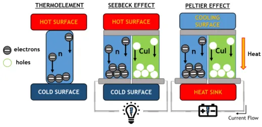
Society has been evolving towards optimising alternative energy sources by increasing its efficiency and reliability to avoid continuous usage of fossil fuels. Thermoelectricity is undoubtedly the case: a reliable and green energy converter; with no noise or vibration as there are no mechanical moving parts; no mechanical fluid, light in weight; and can be powered by direct current. Hence, thermoelectric devices do not require constant maintenance. Life-time testing has shown the capability of thermoelectric devices to exceed 100.000 h of steady-state operation[1],[2].
The Seebeck Effect, discovered in 1821 and named after its Estonian creator – Thomas Seebeck, is a phenomenon seen in thermoelectric devices in which thermal energy from a temperature gradient is converted into electric energy. The reverse effect, known as Peltier Effect, was discovered in 1834 by the French physicist Jean Charles Peltier. Both, Seebeck and Peltier effects, can also be seen in single thermoelectric elements. Nevertheless, a pair of thermoelectric materials (thermoelectric generator (TEG)) is often used to cool down or heat up another surface. In practice, TEGs are often connected electrically in series and thermally in parallel to form a module [1], [2].
Figure 1.1: Thermoelectric devices overview.
2
1.2
Thermoelectric behaviour of a material
The thermoelectricity of a material is described by a dimensionless quantity known as figure of merit (zT), given by (1), where α is Seebeck coefficient (V.K-1), σ is electrical conductivity (Ω-1m-1), T is absolute
temperature (K) and k is thermal conductivity (Wm-1K-1) of a given material which is the sum of lattice thermal conductivity, kL and electronic thermal conductivity ke.[7] Therefore, maximising the figure of
merit is crucial in the selection and optimisation of thermoelectric materials.
𝑧𝑇 =𝛼2𝑘𝜎𝑇 (1)
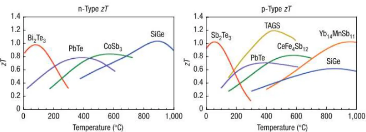
Conventional thermoelectric materials are bulk alloy materials such as Bi2Te3, PbTe, SiGe and CoSb3,
among which Bi2Te3 is the most commonly used one. They usually have a zT value slightly below one[8].
Figure 1.2: state-of-the-art thermoelectric bulk materials figure of merit (zT) over temperature range.
Source: [6]
There are two fundamental properties for a material to be thermoelectric: a) electron and holes transporting heat (ke) and b) phonons travelling through the lattice (kl). These two are both related over
the following equation[9]:
𝑘 = 𝑘𝑒+ 𝑘𝑙 (2)
To obtain a high value of zT the following is required: a low lattice thermal conductivity where phonons have reduced mobility (e.g. as in a glass); charge carriers with higher mobility than those seen in classy materials, and lower effective mass (e.g. as observed in crystalline semiconductors). Since Seebeck and thermal conductivity are directly proportional to figure of merit (equation (1)), one can extrapolate the zT value by using Power factor (PF):
𝑃𝐹 = 𝜎𝛼2 (3)
Thus, very often, good thermoelectric materials are crystalline materials that scatter phonons without compromising electrical conductivity. Since phonons (and photons) vary in a wide spectrum of wavelengths, it is essential to create different mechanisms for the scattering of phonons at different scale lengths – either by introducing numerous interfaces, point defects at interstitials, vacancies or by alloying[6],[10].
3 but simultaneously it also increases the thermal conductivity, while Seebeck coefficient decreases. Therefore intermediate carrier concentration are the most suitable to reach high zT as represented in figure 1.3 [11].
Figure 1.3: zT vs Carrier Concentration. Involves a compromise of thermal conductivity and Seebeck
coefficient with electrical conductivity.
[6]
The thermoelectric performance of a material depends largely on the electronic structure near the Valence Band Maximum (VBM). For example, the case of CuXO semiconductors: its p-type conduction
is originated from the presence of negatively charged Cu vacancies and the dominant Cu 3d10 states near the VBM[12]. The latter enables a more dispersive valence band compared to other metal oxides, which creates a less localised hole-transport pathway.[13]
1.3
Transparent Conductive Semiconductors
In Thin-film (TF) technology, until 2008 not many studies on p-type CuxO TF were reported due to lack
of p-type oxide semiconductors and rigorous fabrication conditions[13]. Cu-based oxides, such as copper oxides, have shown to be promising p-type oxide candidates – with two main types: Cu2O and
CuO – due to their non-toxicity, low cost, and abundancy[14].
Electrical conductivity combined with transparency was first shown by Karl Bädeker in 1907 [15] during the preparation and electrical characterisation of cuprous iodide (CuI) as well as other semiconductor materials. CuI was then the first of this generation, being only 20 years later recognized as a p-type transparent semiconductor [16]. This class of materials is characterised by a wide band gap (>3 eV), a high concentration of charge carriers (>1019 cm-3 ) with moderate mobility (~1 cm2V-1s-1 ).[17]
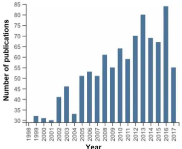
4 2010. However, in terms of CuI application to thermoelectrics only one publication was made as far as was possible to find by our search facilities.
Figure 1.4: Number of publications in the field of Physics, Materials Science and Engineering containing
“CuI” in the title. Data from Thomson Reuters Web of Science (WOS).
Therefore, the aim of this project to obtain a transparent p-type thermoelectric material with a
transmittance over 70% in the visible wavelength range with great thermoelectric properties is time
framed and challenging. CuI thin films were prepared by several methods and its thermoelectric and optical properties evaluated. Several parameters were considered, such as: thin film thickness of initial deposited copper layer, and posterior copper exposure time to iodine; for samples prepared by CuI thermal evaporation, film thickness was varied and a posterior heat treatment was considered. With regards to thermoelectric properties, this project aimed at a Seebeck coefficient value above
200 μVK-1 and a conductivity above 500 Ω-1m-1. For this, besides single element measurements, element
area was also varied as well as the distance between contacts at cold and hot regions. Furthermore, a power factor value in the order of 10-4 Wm-1K-2and a resistance below 5kΩ was the aim. Finally, this
project also investigated p-type CuI thin films applied to different thermoelectric configurations, including multiple thermoelements in series and p-n junctions with gallium doped zinc oxide (GZO).
1.4
Cuprous iodide
CuI different phases. Cuprous iodide (CuI) is a stable solid material known to exist in 3 different phases:
(i) the low temperature zinc-blende structure (-CuI), stable below 370oC, (ii) wurtzite structure (β-CuI)
between 370 °C to 390 °C and (iii) rock salt structure (α-CuI) above 390 °C [18]. The stable cubic structure makes it easy to synthesize CuI thin films near room temperature using a number of chemical and physical methods, including vapour iodisation thermal evaporation [16], pulsed laser deposition (PLD) [19] and sputtering [20]. It is possible to improve the hole conductivity further by appropriate iodine doping [21].
Electrical properties.-CuI is a semiconductor material with a high reported hole mobility
5 cm3) with, at the same time, a heavy hole band. Its high conductivity (σ > 280 Scm-1) [22], and large
Seebeck coefficient (237 μVk-1 for a hole concentration of 1020 cm-3) [7] entail to a good figure of merit.
Its p-type conductivity is originated from copper vacancies, which introduce an acceptor state above the VBM [22],[21].
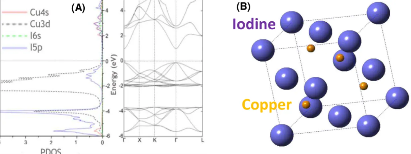
Cuprous iodide flat band at VBM is quite similar to the Cu mentioned above: composed by anisotropic and localized oxygen 2p orbitals, which results in a “light” hole effective mass of 0.3 mo [22]. It also has
a heavy hole band, mainly due to copper 3d10 and iodine 5p that create an acceptor state at Figure 1.5
(A). Thermal conductivity (k) is essential to maximise the thermoelectric potential of a material. Yang et al.[22], reported a value of k of 0.55 W m-1 K-1 at room temperature (by 3ω method), which is lower than
that of glass – reference as a thermal insulator. This happens because of the heavy element iodine, that vibrates less, as well as the strong phonon scattering due to the polycristalline structure of -CuI [7],[21]. The value of zT is estimated up to 0.21 at 300 K and reaches a saturation point at p > 5x1019 cm -3 [22].
Transparency of CuI. The wide direct band gap of CuI allows for a high transparency in the visible
spectral range, where interference fringes relate to the materials thickness by:
2𝑛𝑑 = 𝑚𝜆
(4)where n is the film refraction index, d is the thickness, m is the number of peaks in the wavelength range used for calculation and λ is the incident wavelength. Yang et al., and other reports demonstrate this relationship for CuI with a transmittance ~60-80% over the visible and near-infrared (NIR) spectral ranges and a corresponding 3.1 eV band gap at room temperature.
Figure 1.5: γ-CuI partial density of states (PDOS) and respective band gap distribution. Source: Yadav, M. K.
& Sanyal[7]. CuI structure reproduced by software CrystalDiffract.
(A)
(B)
Iodine
7
2
Materials and Methods
2.1
Samples preparation
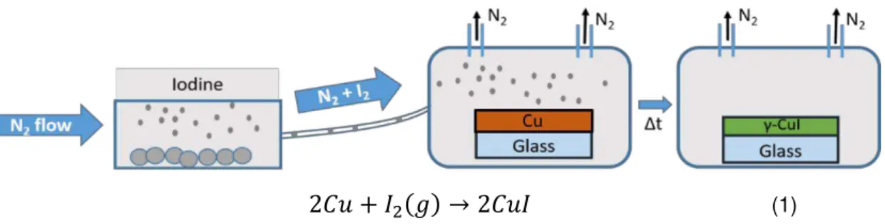
Three different methods were used to deposit CuI layers onto corning glass substrates: thermal evaporation, vapour iodination and solid iodination.
CuI powder (from Sigma Aldrich purity >99.5%) was evaporated in a vacuum chamber (pressure below 10-5 mbar) and a resistive crucible of tungsten. The film thickness (300-400 nm) and deposition rate was
controlled by varying current applied to the crucible (70 to 85 A) and by monitoring the quartz crystal reader. The same method was applied to obtain the Cu films used for iodination. Copper pellets (from Plasma Materials and purity > 99,9%). The Cu films with thicknesses ranging from 100 to 400nm were placed in a plastic box with the Cu layer facing up. Thereafter, N2 vapour transported solid iodine vapour
particles to the sample, iodinating it. Iodine was used as received from PanReac AppliChem. No further purification was needed.
A schematic of the vapour iodination process is depicted in figure 2.1. The optimisation of the process was carried out, varying initial copper thickness from 20 to 100 nm, and iodine exposure time, from 1h to 4h. The corresponding chemical reaction is below, (1), the solid Cu film reacts with iodine forming a transparent CuI solid film. The iodine particles (highly volatile) are trailed by the N2 gas and in contact
with Cu film it starts the iodination process - vapour iodination process.
The solid process schematics are shown in figure 2.2. The box is first filled with N2 gas then solid iodine
pellets are introduced to contact directly with Cu thin films faced up. The box is sealed immediately and kept at room temperature. The chemical reaction that occurs is the same as the following method, with the only exception of iodine being in the solid state. These reactions are visible at the naked eye since the mirror-like sample gradually becomes transparent. The iodination reaction time varied from 30 to 120 minutes.
Figure 2.2: Solid iodination schematic
2𝐶𝑢 + 𝐼
2(𝑔) → 2𝐶𝑢𝐼
(1)8
2.2
Characterization
2.2.1 Optical Measurement
A Jasco V-770 spectrophotometer was used to obtain the transmittance, absorption and reflectance of CuI samples. A beam was emitted against the sample, at a range of wavelength varying from 200nm to 2500nm and its transmittance is read through a sensor. The baseline was systematically corrected against a Corning glass substrate.
2.2.2 Thermoelectric properties measurement
Seebeck coefficient, conductivity and resistance were measured in a homemade apparatus. Samples were placed on top of two Peltier one warming and the other cooling down. Bare Conductive® Carbon ink or silver contacts separated by 3mm was deposited on the film. Simultaneously, a thermal camera (FLIR A310) was used to measure the temperature gradient between contacts (accuracy of 0.1ºC) which in turn was varied by the heating and cooling of the two Peltier
elements under the sample. 2.2.3 Raman
Raman analysis was carried out by a Witec Alpha 300 RAS with Argon Laser with Laser incidence wavelength λ = 543 nm and Laser Power = 15 mW, at DCM-FCT/UNL. Atomic Force Microscopy (AFM) was performed in the same equipment to determine the roughness of samples.
2.2.4 Morphology Analysis
Surface Morphology and elementary composition of the samples were characterized by a scanning electron microscope (SEM - Hitachi S2400 with Bruker light elements EDS, at MicroLab-Electron Microscopy Laboratory of Instituto Superior Técnico). The
samples were placed in the sample holder using a carbon ribbon and then covered with a very thin layer of gold and palladium. Samples thickness and surface roughness mapping were measured in a Perfilometer KLA Tencor D-600, available at DCM – FCT/UNL.
2.2.5 X-Ray Diffraction
X-ray diffraction (XRD - PANalytical X’Pert PRO equipped with an X’Celerator detector using CuKα radiation at 45 kV and 40 mA, in a Bragg–Brentano configuration) was used to analyse the crystalline phases present in the deposited films. XRD patterns were collected over the angular 2θ range 10º-90º with a scanning step of 0.03° at CENIMAT-I3N, FCT-UNL.
2.2.6 Hall-effect
The mobility, concentration and type of major carriers were determined by a Nanometrics HL5500 Hall System equipment being applied 0.1T for the magnetic field and contact geometry factor of 0.99.
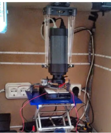
Figure 2.2: Photograph of the
10
3
Results and Discussion
In the following will be presented and discussed the results of CuI samples obtained by the methods investigated: vapour and solid phase iodination and thermal resistive evaporation of CuI powder. The structural, compositional and morphological characterization was performed by X-ray diffraction, Raman, AFM, SEM and EDS. The electro-optical performances were evaluated by UV-VIS-NIR spectroscopy, Hall Effect and thermoelectric characterizations.
3.1
Composition, Structure and Morphology
3.1.1 Structure: X-Ray Diffraction
Figure 3.1: X-Ray Diffraction (XRD) comparison between the three methods depicts X-ray diffraction patterns consistent with literature [23]. At 25º, a peak is given to (111), visible in all samples suggesting it is the predominant growth direction for thermal evaporated and vapour sample, which respective crystallite sizes are 38.7 nm and 46.0 nm. At 30º is visible a small shoulder consistent with (200) planes and at 42º a peak assigned to (220) diffraction planes, most intense for solid sample suggesting this method has a more abrupt transition from copper to copper iodide, suggesting predominant growth for this direction. At 50º, a peak of (311) diffraction planes is also present and at 53º the (222) planes. The main diffraction plans show sharp peaks revealing a high level of crystallinity. No peaks related to pure Cu or CuxOy were
identified indicating a high level of purity. Hence, the results obtained suggest that because solid and vapour iodinated methods have bigger tendency to form CuI (111) and (220). Most likely related to having a previous step of copper deposition, that grows predominantly as Cu (111) and (220) in this lab conditions. Cu XRD for comparison.
Figure 3.1: X-Ray Diffraction (XRD)
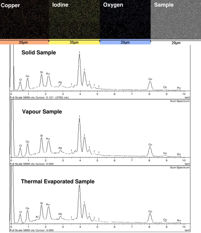
11 3.1.2 Composition: Energy Dispersive Spectroscopy (EDS)
EDS of figure 3.2 shows composition mapping through the sample where Iodine, Copper, Oxygen and Silicon (from the glass substrate) are the most abundant (as predicted). Emission relative percentages of Iodine (~59%), Copper (~36%) and Oxygen (~5%) was obtained, for all methods. The oxygen present on the sample is resultant from the silicon substrate and adsorbed by the CuI film.
Au Cu I I I Pd I O Cu Cu Au Si I I
0 1 2 3 4 5 6 7 8 9 10
keV Full Scale 5899 cts Cursor: 0.121 (3762 cts)
Sum Spectrum Au Cu I I I Pd I O Cu Cu Au Si I I
0 1 2 3 4 5 6 7 8 9 10
keV Full Scale 5899 cts Cursor: 0.000
Sum Spectrum Au Cu I I I
Al Pd I
O Cu Cu
Au
Si I
I
0 1 2 3 4 5 6 7 8 9 10
keV Full Scale 5899 cts Cursor: 0.000
Sum Spectrum
Figure 3.2: EDS spectra for samples produced by solid, vapour and by thermal evaporation methods. Gold
and Palladium were used as a coating in SEM and Silicon is from glass substrate. The uniformity of
elements emission is shown for solid sample. Other EDS surface distribution can be observed in annex.
Solid Sample
Thermal Evaporated Sample
Vapour Sample
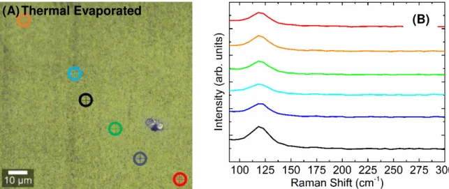
12 3.1.3 Composition: Raman
Figure 3.3 (A) shows a microscope image obtained in the Raman equipment and the excited regions as coloured circles (Figure 3.3 (B)) A homogeneous film surface is observed consistent with Raman spectra. The peak at 120 cm-1 is assigned to transverse optical (TO) mode of Cu-I bonding vibration in
CuI films according to literature [24]. Smaller intensity in the green spectrum (green marker) is associated to lower initial Cu thicknesses, since the whole peak intensity was quantitatively less and laser power was kept constant.
Figure 3.3: CuI vapour sample Raman Spectroscopy: (A) microscope image Magnification x100 of the
sample which coloured markers are respective to the coloured plot in (B). From 300 cm-1 forward, no peaks
were observed.
Figures 3.4 and 3.5 display similar Cu-I Raman peaks as vapour iodinated samples. Main peak at 120cm-1 due to longitudinal optic (LO) vibration, meaning that no chemical differences are observed for
the material prepared by the three methods.
Figure 3.4: Thermally Evaporated CuI Surface Analysis and Raman Spectroscopy. (A) microscopic image
Magnification x100 of the thin film surface and different coloured markers points characterized by Raman
Spectroscopy in (B). In (C) zoom of the oxidation peak at 485cm-1.
(A) Vapour
(B)
13 Figure 3.5: Solid iodination Surface Image and Raman Spectroscopy. (A) X100 magnification microscopic
image of the thin film surface and different coloured crosshairs used to evaluate Raman Spectroscopy
(B).
3.1.4 Morphology: Scanning Electron Microscopy
The surface morphology shown in SEM images of figure 3.6 is characteristic of solid crystallites of iodine. Probably over saturating the upper surface of the CuI sample. Homogeneity of average grain sizes is kept throughout the both samples. On (A), the sample appears (as confirmed by XRD) crystalline, although the roughness of its surface at a nanoscopic level may contribute to light scattering and thus lower transmittance/transparency. On (B), sample solid iodinated has smaller grain size than the previous. In principle, this could mean that there are more grain boundaries, and therefore, the samples of solid method sample are less transparent. The vapour method shows a rougher surface than that of the solid method. Compared to vapour and solid methods, samples from thermal evaporation show smaller grains – although defects are also visible throughout the sample most likely due to the non-stoichiometry of the process. Indeed, the grains are only visible in the higher magnification image (B) with also a few gaps and holes possibly formed during the evaporation process where a rapid sublimation and subsequent crystallisation occurs at different rates (heating vs cooling rate, possibly causing film micro-cracks). The small grain size and compact films may explain its higher transmittance of the sample in the visible range of the spectrum when considering light scattering due to surface roughness.
14
Figure 3.6: SEM images: (A) vapour iodinated sample- X10,000 magnification; (B) SEM image of sample
prepared via Solid Iodination.- X10,000 magnification; (C) thermal evaporation samples magnified to
X10,000 and (D) to X30,000.
3.1.5 Morphology - Atomic Force Microscopy (AFM)
Figure 3.7: AFM 3D Images of solid iodination of copper iodide methods.
Surface roughness of samples prepared by solid iodination presented 28.8 nm whereas vapour iodination showed 85.8 nm and thermal evaporation showed 17.8 nm. This was obtained by AFM.
(C) Thermal Evaporated
(D)T. Evaporated X30.000
(A) Vapour
(B) Solid
15 3.1.6 Optical Transmittance
The photographs of samples produced by the different methods are shown in figure 3.8, where is highlighted its high transparency although some differences in the diffused light is also seen.
Figure 3.8: Photography comparison of the three methods. Sample (A), (B) and (C) were prepared via
Vapour iodination, Solid Iodination and Vapour iodination methods, respectively.
Sample (A) is more translucent than the others. Sample (B) and (C) have a colour gradient due to a thickness gradient created in the initial process of resistive thermal evaporation of copper. Vapour samples show transmittance lower than the ones obtained by solid or thermal evaporation methods.
Figure 3.9 A comparison of Specular Transmittance (A) and Reflectance (B) of the three preparation
methods. (C) represents the plot for band gap estimation through absorption coefficient (α) for vapour
preparation method.
An indirect way of estimating the optical band gap is by extracting the wavelength at which there is a transmittance minimum (see in Figure 3.10(A.1), minimum at 410 nm), that links to an absorption maximum. In the band diagram, the absorption maximum is at an energy where the highest number of electrons can make the transition from the valence to the conduction band. This corresponds to the energy gap that separates both band limits. The energy calculation is represented by the following equation:
16
𝐸 =
ℎ𝑐
𝜆
(5)where E is energy (J), h is Planck’s constant (6.626x10⁻³⁴ J.s), c is the light velocity in vacuum (2.998x10⁸ m.s-1) and λ is the incident light wavelength (m). If λ is 410 nm, equivalent energy is 3.03 eV
(4.84x10⁻¹⁹ J). This value is correspondent to the copper iodide optical band gap, which is slightly
different from values (3.1 eV), reported by Yang, C. et al.[22].
Another approach to obtain band gap energy is by the derivative of absorption coefficient [25]. Such as the maximum value corresponds to the energy band gap value. The energy band gap (Eg) can be
calculated by equation (6) as well, for direct band gap semiconductors, where A is a constant and α the absorption coefficient.
𝛼ℎ𝜐 = 𝐴(ℎ𝜐 − 𝐸
𝑔)
1/2 (6)From both methods the 3.04 eV corresponds to the band gap energy. For solid and thermal evaporated samples the band gap is similar. Tauc’s calculation is in annex (Figure 6.4: Tauc approximation to the Energy Band gap.)
Figure 3.10: (A) shows specular transmittance of Vapour deposited films for different times of iodination.
Inset (A.1) zoom-in at 350 to 430nm wavelength range and extrapolated band gap energy. (B) shows the
variance of transmittance when changing the initial copper thickness for an iodination time of 2h. And (B.1)
represents the zoom-in at 320 to 420nm wavelength range.
In figure 3.10, samples show transmittance values above 60% in the wavelength range of 500-2500nm. When light strikes the film the difference in refractive index of the different media promotes multi-reflections at interfaces. That is visible in the transmittance/absortance spectra by interference fringes. Equation (3) (see Introduction 1.4: Cuprous iodide) relates the number of interference fringes Δm with thin film thickness (d). Thus, it will be visible an increase on the number of interference fringes with the increase of thickness. That is visible in Figure 3.10 (A) where the number of fringes increases with Cu film thickness.
17 Figure 3.11: (A) Specular Transmittance of CuI solid iodinated in three different thicknesses. (B) zoom-in at
300-450nm wavelength scale.
3.2
Fluorescence
The excitation and emission spectra are shown in figures 3.12 respectively for vapour and solid iodination.
Figure 3.12: Fluorescence Spectroscopy for Vapour method. (A) shows the emission spectrum when light
different wavelengths hits the material. (B) represents the excitation spectrum when it emits at 340nm.
The sample emits photons majorly in the blue region of the visible spectrum. Several other excitation wavelengths were tried and the most intense emission is at an excitation wavelength of 275nm (4.5eV), which is well above the energy band gap, ensuring a larger number of electrons populating the conduction band.
18
Figure 3.13: CuI solid iodinated Fluorescence Emission and Excitation spectrum.
The emission and excitation spectra of CuI solid iodinated also shows a strong emission in the blue region of the visible spectrum at an excitation wavelength of 275nm. Other excitation wavelengths were also tried but the optimal, more intense, was at 275nm. However, solid sample show a higher intensity of emission which is maybe related to less defects that trap the photons since optical properties are similar.
3.2.1 Hall Mobility
The hall mobility as a function of carrier concentration is plotted in figure 3.14.
Figure 3.14: Charge carrier concentration over hall mobility for all three methods. Measurements preformed
with Hall Effect measurer. One can see the tendency visible in a normal Hall mobility vs Hole Density plot.
The trend line obtained by our experimental data depicts a higher hole mobility for the same hole density for Thermal Evaporation method. Followed by Solid Iodination and Vapour Iodination. Copper iodide hall mobility trend reported by Grundmann et al.[16], shows similar values. Such data can empirically be fitted for many semiconductors following Masetti et al.[26]:
𝜇
𝑃= 𝜇
𝑚𝑖𝑛+
𝜇
𝑚𝑎𝑥− 𝜇
𝑚𝑖𝑛( 𝑝
𝑝
𝑟𝑒𝑓
)
𝛼
(7)
(A)
(B)
Charge Carrier Concentration (cm-3)
19 Where μP is the hole mobility,μmin andμmax are the maximum and minimum value of mobility reported, p
is the hole density and PREF is an empirical value for CuI (for further information, [16]). The physical
mechanism responsible for the decrease of mobility with increasing hole density is scattering of charge carriers by ionization in the lattice.
3.2.2 Electrical Properties
Figure 3.16 depicts resistance increase over time and PF tends to decrease showing the lower values of resistance and maximum highest Power Factor to 2h, revealing to be the best in terms of electrical properties (see Figure 6.2 in annex for further data).
Figure 3.15: CuI Vapour iodinated samples Resistance, Power Factor and Seebeck over iodine exposition time.
The variation of the electrical and thermoelectric properties of thermal evaporated and solid samples can be seen in table 1 and 2.
Table 1: CuI thermally evaporated electrical properties variation with TF thickness.
Material Thickness (nm) Resistance (kΩ) Conductivity
(103Ω-1m-1)
Seebeck
(μV/K)
PF
(10-5 Wm-1K-2)
CuI Thermal
Evaporated
80 2.8 1.8 158.1 4.5
50 4.7 1.2 261.3 8.2
150 6.8 3.7 189.6 1.3
𝐗̅ - - 1.2 ± 0.6 203 ± 43 4.6 ± 2.8
With a PF in the order of 10-5 and resistances not lower than 2 kΩ down to 10-7, this method reveals the
least adequate properties for this application, in comparison to other methods. Some degree of iodine deficiency has been previously reported by Yamada, et al.[14]. Thermal evaporated I/Cu atomic ratio is
20 different from other deposition methods introducing non-stoichiometry to the deposited films, leading to lower electrical properties. [27], [28].
Table 2: Solid CuI Electrical Properties with same initial Cu thickness.
Material Thickness
CuI (nm)
Resistance
(kΩ)
Conductivity
(103Ω-1m-1)
Seebeck
(μV/K)
PF
(10-5 Wm-1K-2)
CuI Solid
380 1.6 3.7 156.0 9.2
410 4.3 1.8 206.0 7.7
420 0.8 1.2 145.0 2.4
𝐗̅ 403 ± 12 2.0 ± 1.1 2.23 ± 0.75 169.0 ± 18.8 6.4 ± 2.1
With a CuI film thickness increase, PF reaches an order of magnitude in the 10-5 W/m.K2 and the
resistance of the film is lower than in previous method.
Table 3: All methods electrical properties
Resistance (kΩ)
Thickness (nm)
Conductivity
(Ω-1m-1)
Seebeck
(μV/K)
PF
(10-5 Wm-1K-2)
Vapour 4.2 ± 1.2 426 ± 31 568 ± 126 161 ± 9 1.3 ± 2.1 T.Evap 4.8 ± 1.2 93 ± 30 1119 ± 412 203 ± 31 4.6 ± 2.0 Solid 2.2 ± 1.5 403 ± 18 2233 ± 797 169 ± 86 6.4 ± 2.8
The solid iodination method shows a higher PF value and a lower resistance, when comparing to other methods. Also, with a highest value of hole density and hall mobility, this method quickly became the preferred for the preparation of CuI film samples.
21
3.3
Thermoelectric Generator
To test the viability of power generation combining p-type transparent CuI films with a n-type transparent and conductive oxide (GZO was chosen as it was available to be deposited by sputtering at the lab) we have made p-n single and double thermoelectric modules with carbon contacts 1mm apart.
3.3.1 Power curves
Before the modules characterization single CuI and GZO elements were tested, as shown in figure 25. The CuI TE element shows a typical IV and PV curves with a maximum power of 0.54 nW for 13ºC ΔT. For the same gradient N-type GZO presents up to 0.2 nW. Comparing the potential over current curve, the open circuit voltage (VOC) of CuI is 2.2 mV and of GZO is 0.8 mV. Hence, the device output resistance
for CuI is 0.6 nΩ, whereas for GZO it is 0.02 nΩ. When combining these two elements in a p-n module, at the same temperature gradient 13 ºC a maximum of 0.7 nW and a VOC of 3.3 mV is obtained which
is slightly higher than the sum of the previous values, maybe due to some non-uniformity of samples. Adding another p-n module in series (two p-n module) a maximum power (at T=13ºC) of 1.2nW and Voc of 6.5 mV was obtained, that is, the values almost duplicate, as expected.
Figure 3.16: Power curves for the following thermoelectric elements CuI, GZO, CuI/GZO p-n module and 2
p-n modules in series. Temperature gradient (ΔT) of 6, 11 and 13ºC created between carbon contacts,
distanced 1 cm.
22 thermoelements in series – [1], [2] and [3]; varied the distance between contacts – [4] and [5]; And varied the area of each unit without changing the distance between electrical contacts – [6], [7], [8]
and [9].
Figure 3.17: Map of thermoelectric effect study. Each number corresponds to a thermoelement (constituted
by two parts). Table relates to the area of each part of a thermoelement. [1], [2] and [3] focus on combining
thermoelements in series. In [4] and [5], varying the distance to the electrical contacts. In [6], [7], [8] and [9]
the area was varied and the distance to the contacts kept. The study made in lab are in Figure 6.5
3.3.2 Varying dimensions
23 Figure 3.18: Potential difference vs Temperature gradient study when varying (i) contacts distance; (ii)
Length; (iii) number of modules electrically in series and (iv) Dimensions specified on the schematic image.
2 4 6 8 10 12 14 16
0.5 1.0 1.5 2.0 2.5 3.0 3.5
4.0 1 pn module
2 pn modules 3 pn modules
V
(mV
)
2 3 4 5 6 7 8 9
0.4 0.6 0.8 1.0 1.2 1.4 1.6 1.8 2.0 2.2 V (mV)
2.0 cm
21.5 cm
21.0 cm
22 3 4 5 6 7 8 9 10
0.6 0.8 1.0 1.2 1.4 1.6 1.8 2.0 2.2 2.4 0.5 cm2
1.5 cm2 2.0 cm2
V
(mV)
(i) Varying CD
(iii) Increasing TE
modules
(ii) Varying Length
24
4
Conclusions
This dissertation has focused on the optimisation and characterisation of -CuI thin films: a promising is seen nowadays, such as in transparent thermoelectrics. -CuI thin films of 100-300nm in thickness were prepared by three methods: Vapour Iodination and Solid Iodination of a Cu thin film, and Thermal Evaporation of powder CuI. In spite of their similar morphological and chemical composition, each method reveals different optoelectronic properties. As such, this project focused on the optimisation of such properties in the view of its intending final application for transparent thermoelectrics. Characterization techniques included X-Ray Diffraction, Scanning Electron Microscopy coupled with Energy Dispersive spectroscopy, Raman spectroscopy and Photoluminescence; accompanied with measurements of Seebeck, conductivity, charge carrier mobility and density.
X-ray diffraction characterisation was made and each peak identified revealed the dominant crystalline
planes of CuI (111) and (220). Thermal Evaporation had more intense peaks, (111) plane is the predominant growth plane with corresponding crystallite size of 38.7 nm. Vapour Iodination predominant peak is (111), and the second more intense is of (220) planes. Solid method shows that the predominant peak is (220) which is believed to be related to the abrupt iodination by the solid iodine particles, not leaving enough time for the formation of the (111) plane, which then becomes the second most preponderant growth plane for this method.
Energy Dispersive Spectroscopy analysis have shown the existence of Iodine, Copper, Oxygen and
Silicon (from the glass substrate). All three methods show similar emission relative percentages of Iodine (~59%), Copper (~36%) and Oxygen (~5%).
SEM images depict different grain sizes for each method. Difference between darker and brighter
colours given to roughness of the sample, which is more intense for vapour method samples and a respective surface roughness of 85.8 nm and grain size of 186 nm. Solid method grain size is around 112 nm and roughness of 28.8 nm. Thermal evaporation shows the smallest grain size (44 nm) and corresponding surface roughness of 17.8 nm. Roughness suggest an explanation for vapour samples to be less transparent than that of solid and thermal evaporation samples related to their light scattering.
Raman spectroscopy allowed to detect bond vibrations along the surface upon excitation with a laser
at 532nm wavelength. All samples demonstrate peaks at 120 cm-1 which correspond to Cu-I bonds. The
thermal evaporation method also showed some variations throughout the sample that are related to defects imposed by the non-stoichiometry of the physical vapour deposition method, which sublimes CuI powder of constituents with different vapour pressures and rates of sublimation vs. cooling and thus causing material dislocations/microcracks after deposition.
Energy band gap was estimated via the optical absorption coefficient using the transmittance spectrum
25
Electrical properties aimed at the start of the project were achieved. The solid iodination method originates reproducible films with a PF in the order of 10-4 Wm-1K-2. In terms of their power factor, vapour
iodinated samples are not as good as other methods, since PF values ranged from 10-5 to 10-7 Wm-1K-2
with 2h of iodine exposure time. Although with intermediate values of PF, the non-stoichiometry of thermal evaporated samples proved difficulty in reproducibility of results.
Fluorescence, samples emit photons majorly in the blue region of the visible spectrum. Several other
excitation wavelengths were tried and the most intense emission is at an excitation wavelength of 275nm (4.5eV), well above the band gap.
Power curves, a noticeable difference is seen between CuI p-type and GZO n-type in thermoelectric
modules. CuI has shown higher values of VOC and Power than GZO. A more appropriate n-type material
could have been used to outperform this study. 2 p-n modules reached the maximum VOC of 6.5mV
which is a very good value when comparing to other commercial devices. Carbon contacts are more appropriate for longevity testing than for electrical testing, proving themselves constant along time but lacking on electrical properties (lower maximum power output values than with other contacts).
The effect of geometry in Seebeck study shows that there is no considerable change when varying
the area of the samples since Seebeck is an intrinsic property of the material. It also shows that the increase of TE modules leads to an increase of the voltage output (as expected).
This way, a transparent p-type y-CuI layer was optimised and the results proved that the Solid iodination method was better optimised in terms of electrical and optical properties. This low-cost process of CuI thin films fabrication can guarantee a reproducible CuI layer to overcome the current market demands. It has proven to be a good choice for power applications when comparing with other transparent p-type oxide semiconductor materials. Despite its low power output, its high VOC and transparency combination
26
5
Bibliography
[1] S. B. Riffat and X. Ma, “Thermoelectrics: A review of present and potential applications,” Appl. Therm. Eng., vol. 23, no. 8, pp. 913–935, 2003.
[2] D. Zhao and G. Tan, “A review of thermoelectric cooling: Materials, modeling and applications,” Appl. Therm. Eng., vol. 66, no. 1–2, pp. 15–24, 2014.
[3] H. Xi, L. Luo, and G. Fraisse, “Development and applications of solar-based thermoelectric technologies,” Renew. Sustain. Energy Rev., vol. 11, no. 5, pp. 923–936, 2007.
[4] M. Kishi et al., “Micro thermoelectric modules and their application to wristwatches as an energy source,” Eighteenth Int. Conf. Thermoelectr. Proceedings, ICT’99 (Cat. No.99TH8407), no. 1 999, pp. 301–307, 1999.
[5] H. Power, “Energy Harvesting from Human Power,” Energy Harvest. Netw., March, 2011. [6] G. J. Snyder and E. S. Toberer, “Complex thermoelectric materials,” Nat. Mater., vol. 7, no. 2,
pp. 105–114, 2008.
[7] M. K. Yadav and B. Sanyal, “First-principles study of thermoelectric properties of CuI,” Mater. Res. Express, vol. 1, no. 1, p. 15708, 2014.
[8] G. J. Snyder and E. S. Toberer, “Complex thermoelectric materials,” Nat. Mater., vol. 7, no. 2, pp. 105–114, Feb. 2008.
[9] G. V Chester and A. Thellung, “The Law of Wiedemann and Franz,” Proc. Phys. Soc., vol. 77, no. 5, pp. 1005–1013, 1961.
[10] D. M. Rowe, CRC handbook of thermoelectrics. CRC Press, pp. 561-563, 1995.
[11] H. J. Goldsmid and J. W. Sharp, “Estimation of the thermal band gap of a semiconductor from seebeck measurements,” J. Electron. Mater., vol. 28, no. 7, pp. 869–872, 1999.
[12] J. Yu, G. Liu, A. Liu, Y. Meng, B. Shin, and F. Shan, “Solution-processed p-type copper oxide thin-film transistors fabricated by using a one-step vacuum annealing technique,” J. Mater. Chem. C, vol. 3, no. 37, pp. 9509–9513, 2015.
[13] A. Liu et al., “In situ one-step synthesis of p-type copper oxide for low-temperature, solution-processed thin-film transistors,” J. Mater. Chem. C, vol. 5, no. 10, pp. 2524–2530, 2017. [14] N. Yamada, R. Ino, and Y. Ninomiya, “Truly Transparent p-Type γ-CuI Thin Films with High Hole
Mobility,” Chem. Mater., vol. 28, no. 14, pp. 4971–4981, 2016.
27 [16] M. Grundmann, F. L. Schein, M. Lorenz, T. Buntgen, J. Lenzner, and H. Von Wenckstern, “Cuprous iodide - A p-type transparent semiconductor: History and novel applications,” Phys. Status Solidi Appl. Mater. Sci., vol. 210, no. 9, pp. 1671–1703, 2013.
[17] S. R. Kodigala, Thin Film Solar Cells from Earth Abundant Materials. pp. 261-263, 2014. [18] T. Prakash, “Influence of temperature on physical properties of copper ( I ) iodide,” vol. 2, no. 2,
pp. 131–135, 2011.
[19] P. Sirimanne, M. Rusop, T. Shirata, T. Soga, and T. Jimbo, “Characterization of transparent conducting CuI thin films prepared by pulse laser deposition technique,” Chem. Phys. Lett., vol. 366, no. 5–6, pp. 485–489, Dec. 2002.
[20] T. Tanaka, K. Kawabata, and M. C. Hirose, “Transparent, conductive CuI films prepared by rf-dc coupled magnetron sputtering,” Thin Solid Films, vol. 281-282, pp. 179–181, 1996.
[21] C. Yang, M. Kneiß, M. Lorenz, and M. Grundmann, “Room-temperature synthesized copper iodide thin film as degenerate p-type transparent conductor with a boosted figure of merit,” Proc. Natl. Acad. Sci., vol. 113, no. 46, pp. 12929–12933, 2016.
[22] C. Yang et al., “ARTICLE Transparent flexible thermoelectric material based on non-toxic earth-abundant p-type copper iodide thin film,” Nat. Commun., no. May, p. in press, 2017.
[23] Z. Zheng et al., “Growth of highly oriented (110) gamma-CuI film with sharp exciton band,” J. Mater. Chem., vol. 18, no. 8, pp. 852–854, 2008.
[24] J. E. Potts, R. C. Hanson, C. T. Walker, C. Schwab, and U. L. Pasteur, “pp. 389—392, 1973.,” vol. 13, pp. 389–392, 1973.
[25] V. Ariel, V. Garber, D. Rosenfeld, and G. Bahir, “Estimation of HgCdTe band-gap variations by differentiation of the absorption coefficient,” Appl. Phys. Lett., vol. 66, no. 16, p. 2101, 1995. [26] G. Masetti, M. Severi, and S. Solmi, “Modeling of Carrier Mobility Against Carrier Concentration
in Arsenic-, Phosphorus-, and Boron-Doped Silicon,” IEEE Trans. Electron Devices, vol. 30, no. 7, pp. 764–769, 1983.
[27] Y. Peng et al., “Efficient organic solar cells using copper(I) iodide (CuI) hole transport layers,” Appl. Phys. Lett., vol. 106, no. 24, 2015.
28
6
Annex
Figure 6.1: Oxidized Copper Raman Spectroscopy: visible peaks at around 600cm-1 and 1200cm-1
correspondent to CuO and Cu2O vibrational modes.
Figure 6.2: CuI vapour prepared electrical properties. Resistance values were measured at room
temperature in function of iodine exposure time. Resistance increases with iodine deposition and Seebeck
29 Figure 6.3: CuI thermally evaporated electrical properties with and withoutheat treatment (done in Vacuum
or N2 atmosphere) at 100ºC. (B) Specular Transmittance of Thermally Evaporated CuI without and with heat
treatment in two different atmospheres: Nitrogen and Vacuum.
The transmittance increase in the range of 200 to 450nm depicts a lowering of the absorptance due to modification of the lattice after the material is heat treated. Resistance and Seebeck increase with heat treatment and resulting PF is the highest for Heat Treatment in nitrogen atmosphere.
1.0 1.5 2.0 2.5 3.0 3.5 4.0 4.5 5.0 5.5 6.0
2.8 3.0 3.2 3.4 3.6 3.8
(
h
)
2
E (eV)
d(
h
)
2 /dE (a.u.)
E (eV)
Figure 6.4: Tauc approximation to the Energy Band gap.
Figure 6.5: Thermoelectric study made in lab.
30
Copper Iodine
Oxygen Sample
Copper Iodine
(A)
31
Figure 6.6: EDS characterization of sample Copper, iodine and oxygen respective surface emissions.
X100,000 Magnification, prepared by: (A) Vapour Method, (B) Thermal Evaporated method and (C) Solid
method
All these cases demonstrate an homogeneous distribution of the atomic elements of Cu, Iodine along the TF surface area
Oxygen Sample
Copper Iodine
Oxygen Sample

![Figure 3.1: X-Ray Diffraction (XRD) comparison between the three methods depicts X-ray diffraction patterns consistent with literature [23]](https://thumb-eu.123doks.com/thumbv2/123dok_br/16698380.743913/27.892.498.802.366.872/figure-diffraction-comparison-methods-diffraction-patterns-consistent-literature.webp)