HOLOS, Ano 35, v.2, e8192, 2019 1
ANALYSIS OF SILICON CARBIDE POLYMORPHS SUBSTRATES EFFECT ON
PERFORMANCES OF ALGAN/GAN DOUBLE QUANTUM WELL HEMTS
M. SABAGHI
Photonics and Quantum Technologies Research School, Nuclear Science and Technology Research Institute, Tehran, Iran
Received 15/01/2019 – Acepted 28/11/2019 DOI: 10.15628/holos.2019.8192 ABSTRACT
AlGaN/GaN high electron mobility transistors (HEMTs) have established terrific features in the high-power and high-frequency applications of microwave device. In this paper, the impact of silicon carbide polymorphs substrates including 6H-SiC, 3C-SiC and 4H-SiC on the performances of AlGaN/GaN double quantum well HEMTs (DQW-HEMTs) are analyzed and investigated. The results show that the devices with 4H-SiC and 6H-SiC substrates exhibit a higher transconductance of about 192 ms/mm at VDS = 15 V and a lower minimum noise figure (NFmin) of 0.48 and 0.42 dB at 10 GHz than
those of devices with 3C-SiC, respectively. Whereas, DC-HEMT with 3C-SiC substrate has a transconductance of about 180 ms/mm at VDS = 15 V and a minimum noise figure of 3.01 dB at 10 GHz. On the other hands, the DC-HEMT with 3C-SiC substrate has lower drain gate capacitance (Cdg) and higher cut-off frequency (ft) than DC-HEMT with 4H-SiC and 6H-SiC substrates. The results demonstrate that AlGaN/GaN DH-HEMTs 4H-SiC and 6H-SiC substrates are promising devices for future high-power and high-frequency electron device applications.
KEYWORDS: Silicon carbide polymorphss, 6H-SiC, 3C-SiC, 4H-SiC, AlGaN/GaN, Minimum noise figure (NFmin), Double quantum well, High electron mobility transistors (HEMTs).
HOLOS, Ano 35, v.2, e8192, 2019 2
1. INTRODUCTION
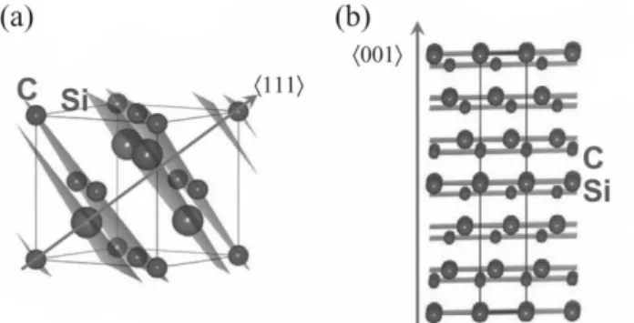
The crystal lattice of silicon carbide material is similar to silicon and diamond where its lattice sites are filled equally by the silicon atoms and carbon atoms. The silicon carbide polymorphs are very stable and useful for high-power, high-frequency, and high-temperature electronics and optoelectronic devices. It should be mainly because of the wide band gap, high thermal conductivity, high breakdown electric field strength, high-saturated drift velocity and high thermal stability. In one hand, the wide band gap causes the high electric fields and the reduction in intrinsic carrier concentration. On the other hand, the thermal leakage current in SiC is very lower as well as temperature rises. Therefore, the device can operate at high electric fields and temperatures with reduced power losses and die size (Marjani, et al., 2011b; Marjani and Marjani, 2012a; Marjani, et al., 2012a; Marjani, et al., 2013; Coffa, et al., 2015; Deboy, et al., 2016). The first commercialization of SiC-based devices is the high power Schottky-diodes (Neudeck, et al., 2001). Recently, many different electronic and optoelectronic devices have been demonstrated with silicon carbide include PN diodes, metal-oxide-semiconductor field-effect transistors (MOSFETs), metal-semiconductor field-effect transistors (MESFETs), high electron mobility transistors (HEMTs), tunneling field-effect transistor(TFET) and lasers polytypes (Marjani, et al., 2011a; Marjani and Marjani, 2012b; Marjani, et al., 2012b; Marjani and Marjani, 2012c; Marjani and Hosseini, 2014; Majdabadi et al., 2014; Marjani and Hosseini, 2015; Sabaghi, et al., 2015; Marjani, et al., 2016a; Marjani, et al., 2016b; Sabaghi, et al., 2016; Marjani, et al., 2017). The silicon carbide has many stable polymorphs including cubic zinc-blende, hexagonal and rhombohedral polymorphs. The filled sites with silicon and carbon in a diamond framework result the formation of cubic zinc-blende silicon carbide polymorphs such as 3C-SiC. The silicon-carbon bilayers consisting of carbon and silicon layers stack in the primitive unit cell in hexagonal polytypes and rhombohedral polytypes. Figure. 1 shows the lattice structures of the 3C-SiC and 6H-SiC polytypes (Muranaka, et al., 2008; Marjani, et al., 2012b; Marjani and Marjani, 2012a; Marjani, et al., 2017).
Figure 1: The lattice structures of the 3C-SiC (a) and 6H-SiC (b) polytypes.
AlGaN/GaN HEMTs have served as one of the most attractive candidates for future high-frequency integrated circuits due to its compatibility with the industry-matured silicon
HOLOS, Ano 35, v.2, e8192, 2019 3 complementary metal-oxide-semiconductor (Si-CMOS) integrated circuits technologies. A high-density two-dimensional electron gas (2-DEG) is formed at the heterointerface between AlGaN and GaN layers due to the large offset in conduction band and polarization charge in AlGaN/GaN heterostructures (Guo, et al., 2008).
In the recent years, a lot of research work has been carried out to study the GaN HEMTs including the optimization of GaN-based HEMT devices and integration (Stoffels, et al., 2015; Zhang, et al., 2016; Wang, et al., 2017; Hashizume, et al., 2018; Kim, et al., 2018), the enhancement of reliability (Koller, et al., 2017; Meneghini, et al., 2017; Qi, et al., 2018), the comprehensive device modeling (Raciti, et al., 2014; Radhakrishna, et al., 2015; Cornigli, et al., 2015) and the commercialization designs (Di Cioccio, et al., 2015; Then, et al., 2015; Ishida, et al., 2016; Lidow, et al., 2016). In addition, the development works have been conducted and reported on microwave noise performance of GaN HEMT. The AlGaN/GaN HEMT with 100 nm gate length is reported with minimum microwave noise figure of 1.2 dB at 20 GHz (Haifeng Sun, et al., 2009). A remarkable reduction of the buffer leakage for AlGaN/GaN double quantum well HEMT with high current drive and fast frequency response is reported (Wang, et al., 2012).
In this paper, the impact of silicon carbide polymorphs substrates including 6H-SiC, 3C-SiC and 4H-SiC on the performances of AlGaN/GaN double quantum well HEMTs (DQW-HEMTs) are analyzed and investigated in terms of transconductance, drain-gate capacitance (Cdg), minimum noise figure (NFmin), current gain cut-off frequency and power gain cut-off frequency. The following aspects will be covered: the model in section 2, the device structures in section 3, the performances of structures including radio frequency and noise in section 4 and final conclusion in section 5.
2. MODEL
The Poisson’s equation, the carrier continuity equations and the drift-diffusion transport equations are considered in order to modeling of HEMT operation. The Poisson's equation relates the electrostatic potential to the space charge density and is defined as (Atlas – Device Simulation Framework., 2018):
1
where ψ, ρ and ε are the electrostatic potential, local charge density and local permittivity, respectively.
The carrier continuity equations of electron and hole are defined by (Atlas – Device Simulation Framework., 2018):
(
e y)
rHOLOS, Ano 35, v.2, e8192, 2019 4 2
3
where n, p, Jn, Jp, Gn, Gp Rn, Rp and q are the electron concentration, hole concentration, electron current density, hole current density, electrons generation rate, holes generation rate, electrons recombination rate, holes recombination rate and magnitude of the charge on the electron, respectively.
Another equations in modeling are current density equations that derived by using the drift-diffusion transport equations. The current density equations for electron and hole are defined by (Atlas – Device Simulation Framework., 2018):
4 5
where μn, μp, En, Ep, Dn, Dp, ∇n and ∇p are the electron mobility, hole mobility, electron diffusion constant, hole diffusion constant, three-dimensional spatial gradient of electron and three-dimensional spatial gradient of hole, respectively.
The above-mentioned equations were solved self-consistently together with device simulator ATLAS software (Atlas – Device Simulation Framework., 2018). In order to achieve more accuracy, several models are considered including the Shockley-Read-Hall recombination model, the parallel electric field dependent mobility model and band gap narrowing model.
3. DEVICE STRUCTURE
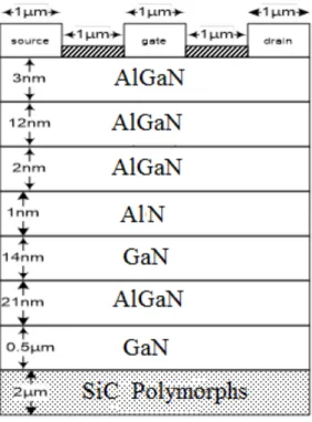
Schematic cross-sections of the AlGaN/AlN/GaN/AlGaN/GaN DC-HEMT structure with silicon carbide polymorphs substrates including 6H-SiC, 3C-SiC and 4H-SiC are shown in Figure. 2.For more details about working principles and advantages of HEMT with the help of band diagrams can be found in (Cornigli, et al., 2015; Ishida, et al., 2016; Zhang, et al., 2016; Koller, et al., 2017; Hashizume, et al., 2018; Kim, et al., 2018; Qi, et al., 2018). The dimensions of the structures are as follows: 1 µm of gate length, 1µm of gate width, source-gate spacing Lsg = 1µm, gate-drain spacing Lgd = 1µm, 1 µm of source length, 1 µm of drain length, 2 µm of SiC silicon carbide polymorphs substrate thickness, 0.5 µm of GaN undoped minor channel and buffer layer thickness, 21 nm of AlGaN undoped back barrier layer thickness, 14 nm of GaN undoped major channel thickness, 2 nm of Al0.3Ga0.7N thickness and, 1 nm of AlN undoped spacer layer thickness, 12 nm of doped carrier supplier layer thickness, 3nm of undoped cap layer thickness and 5.1 eV of gate Schottky contact work function.
1 . n n n n G R J t q ¶ = - + Ñ ¶ !" 1 . p p p p G R J t q ¶ = - + Ñ ¶ !" n n n n n J =qn Eµ +qDÑ p p p p p J =qn Eµ -qD Ñ
HOLOS, Ano 35, v.2, e8192, 2019 5
Figure 2: The Schematic cross-sections of the AlGaN/AlN/GaN/AlGaN/GaN DC-HEMT structure.
The AlGaN layer as bottom barrier is located 14 nm away from the AlGaN/GaN heterointerface. Figure. 3 shows the conduction band energy diagram of the AlGaN/AlN/GaN/AlGaN/GaN DC-HEMT structure. As can be seen from Figure. 3, the conduction band at the AlGaN/GaN interface falls below the Fermi level and thus a minor channel can be formed. However, the most of electrons are located in the GaN major channel.
Figure 3: The conduction band energy diagram of AlGaN/AlN/GaN/AlGaN/GaN DC-HEMT.
4. RESULTS AND DISCUSSION
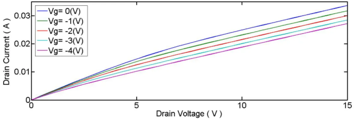
The drain currents with respect to the drain-source voltages of the AlGaN/AlN/GaN/AlGaN/GaN DC-HEMT structure with silicon carbide polymorphs substrates including 3C-SiC, 4H-SiC and 6H-SiC for different gate voltage are plotted in Figures. 4-6,
HOLOS, Ano 35, v.2, e8192, 2019 6 respectively. As seen, the maximum drain currents are about 800, 2500 and 3500 mA for AlGaN/AlN/GaN/AlGaN/GaN DH-HEMT with 3C-SiC, 4H-SiC and 6H-SiC substrates with 0 V of gate voltage, respectively.
Figure 4: The drain current as a function of drain voltage for the DC-HEMT structure with 3C-SiC substrate.
Figure 5: The drain current as a function of drain voltage for the DC-HEMT structure with 4H-SiC substrate.
Figure 6: The drain current as a function of drain voltage for the DC-HEMT structure with 6H-SiC substrate.
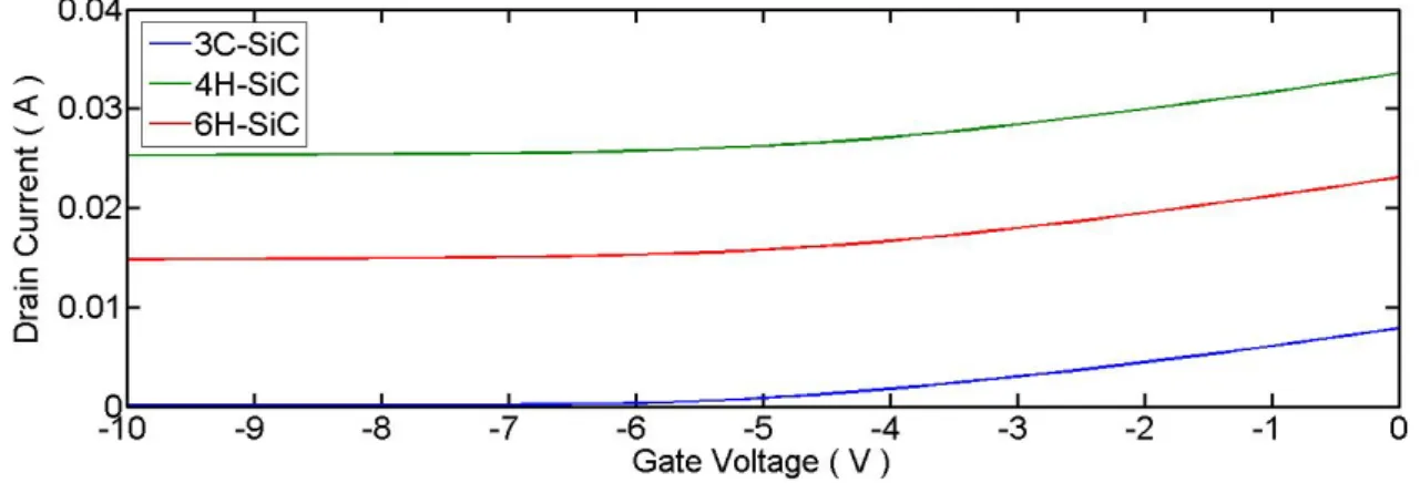
The drain current and transconductance as a function of gate voltage of the AlGaN/AlN/GaN/AlGaN/GaN DC-HEMT structure with silicon carbide polymorphs substrates at 6 V of drain voltage are compared in Figures. 7 and 8, respectively. It is clear from Figure. 7 that the drain current of AlGaN/AlN/GaN/AlGaN/GaN DH-HEMTs with 4H-SiC substrate are higher than
HOLOS, Ano 35, v.2, e8192, 2019 7 those of the AlGaN/AlN/GaN/AlGaN/GaN DH-HEMTs with 3C-SiC and 6H-SiC substrates. This is due to the highly resistive 3C-SiC substrate as the voltage drop on the buffer layer of AlGaN/AlN/GaN/AlGaN/GaN DH-HEMT is mitigated by the partial depletion of the substrate. On the other hand, the trapping effects are stronger with highly resistive 3C-SiC substrate because of the capacitance of the depleted substrate. However, transconductance of AlGaN/AlN/GaN/AlGaN/GaN DH-HEMT with 4H-SiC substrate change slightly compared to the transconductance in the AlGaN/AlN/GaN/AlGaN/GaN DH-HEMT with 6H-SiC substrate, as can confirmed from Figure. 8.
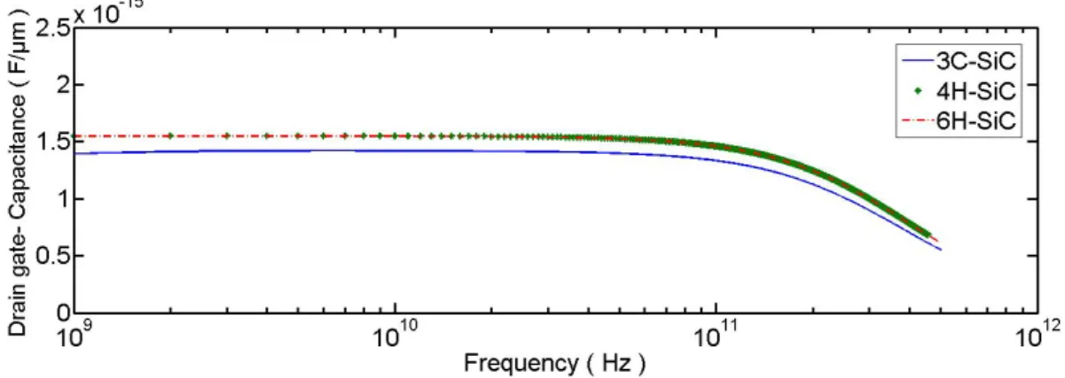
The drain-gate capacitance of AlGaN/AlN/GaN/AlGaN/GaN DC-HEMT structure with silicon carbide polymorphs substrates as a function of frequency at 15 V of drain voltage and -0.2 V of gate voltage are shown in Figures 9. As seen, the value of drain-gate capacitance is almost similar for all silicon carbide polymorphs substrates due to their wide band gap. However, intrinsic carrier concentration decreases exponentially with the energy band gap.
The radio frequency performances of the AlGaN/AlN/GaN/AlGaN/GaN DH-HEMTs are evaluated by cut-off and maximum oscillation frequencies. The cut-off and maximum oscillation frequencies are extracted from current gain cut-off frequency and power gain cut-off frequency
Figure 7: The drain current dependence on a negative gate voltage sweep for AlGaN/AlN/GaN/AlGaN/GaN DC-HEMT structure with silicon carbide polymorphs substrates at 6 V of drain voltage.
HOLOS, Ano 35, v.2, e8192, 2019 8
Figure 8: The transconductance dependence on a negative gate voltage sweepfor AlGaN/AlN/GaN/AlGaN/GaN DC-HEMT structure with silicon carbide polymorphs substrates at 6 V of drain voltage.
Figure 9: The drain-gate capacitance of AlGaN/AlN/GaN/AlGaN/GaN DC-HEMT structure with silicon carbide polymorphs substrates as a function of frequency.
when they drop to unity, respectively. The equations of cut-off and maximum oscillation frequencies are defined by (Sanabria, 2006):
6 7
where, gm, Cgs, Cgd, Rds and Rg are transconductance, source-gate capacitance drain-gate
capacitance, source- drain resistance and gate resistance, respectively.
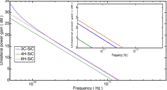
The radio frequency performances of the AlGaN/AlN/GaN/AlGaN/GaN DH-HEMTs including current gain cut-off and power gain cut-off frequencies for silicon carbide polymorphs substrates at 15 V of drain voltage and -0.2 V of gate voltage are plotted in Figures. 10 and 11, respectively. As evident from Figure 10, the values of cut-off frequency are 123.7, 116.7 and 116.8 GHz for the AlGaN/AlN/GaN/AlGaN/GaN DH-HEMTs with 3C-SiC, 4H-SiC and 6H-SiC substrates, respectively. In addition, the values of maximum oscillation frequency are 124, 104 and 129 GHz for the AlGaN/AlN/GaN/AlGaN/GaN DH-HEMTs with 3C-SiC, 4H-SiC and 6H-SiC substrates, respectively.
The minimum noise figure are measures of degradation of the signal-to-noise ratio induced by components in a signal chain and its equations is defined by (Sanabria, 2006):
8
(
)
2 m t gs gd g f C C p = + max 2 ds g R ft f R = min 1 g s gs m R R NF kfC g + = +HOLOS, Ano 35, v.2, e8192, 2019 9 where, Rs k and f are source resistance, fitting factor and frequency of operation, respectively.
Since the gate-source capacitance of structures is nearly constant, the minimum noise figure is inversely proportional to transconductance (Chu, et al., 2005).
Figure 10: The current gain cut-off frequency of AlGaN/AlN/GaN/AlGaN/GaN DH-HEMT with silicon carbide polymorphs substrates at 15 V of drain voltage and -0.2 V of gate voltage.
Figure 11: The power gain cut-off frequency of AlGaN/AlN/GaN/AlGaN/GaN DH-HEMT with silicon carbide polymorphs substrates at 15 V of drain voltage and -0.2 V of gate voltage.
109 1010 1011 1012 0 10 20 30 40 50 Frequency ( Hz ) C u rr e n t g a in ( d B ) 3C-SiC 4H-SiC 6H-SiC 1011.1 1011.2 0 1 2 3 Frequency ( Hz ) Cur r e n t g a in ( d B ) 1010 1011 0 5 10 15 20 25 30 35 Frequency ( Hz ) U n ila te ra l p o w e r g a in ( d B ) 3C-SiC 4H-SiC 6H-SiC 1011.1 1011.2 0 1 2 3 4 Frequency ( Hz ) Un il a te r a l p o we r g a in ( d B )
HOLOS, Ano 35, v.2, e8192, 2019 10
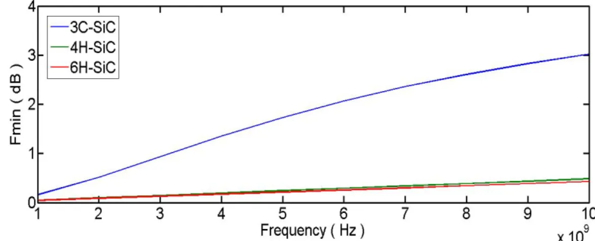
Figure 12: The minimum noise figure of AlGaN/AlN/GaN/AlGaN/GaN DH-HEMT with silicon carbide polymorphs substrates at 15 V of drain voltage and -0.2 V of gate voltage.
Figure. 12 shows minimum noise figure as a function of frequency for AlGaN/AlN/GaN/AlGaN/GaN DH-HEMT with silicon carbide polymorphs substrates at 15 V of drain voltage and -0.2 V of gate voltage. As can be seen, AlGaN/AlN/GaN/AlGaN/GaN DH-HEMT with 6H-SiC and 4H-SiC substrates have lower minimum noise figure of 0.42 dB and 0.48 dB at 10 GHz than AlGaN/AlN/GaN/AlGaN/GaN DH-HEMT with 3C-SiC substrate (NFmin =3.01 dB). It should
be mainly due to the higher transconductance of AlGaN/AlN/GaN/AlGaN/GaN DH-HEMT with 6H-SiC and 4H-6H-SiC substrates than AlGaN/AlN/GaN/AlGaN/GaN DH-HEMT with 3C-6H-SiC substrate. The results demonstrate that AlGaN/AlN/GaN/AlGaN/GaN DH-HEMT 4H-SiC and 6H-SiC substrates are promising devices for future high-power and high-frequency electron device applications.
5. CONCLUSION
This paper focuses on the impact of silicon carbide polymorphs substrates including 6H-SiC, 3C-SiC and 4H-SiC on the performances of AlGaN/GaN double quantum well HEMTs. On one hand, results show that AlGaN/GaN double quantum well HEMTs with 4H-SiC and 6H-SiC substrates have higher transconductance and lower minimum noise figure than the 3C-SiC devices. On the other hand, AlGaN/GaN double quantum well HEMTs with 3C-SiC substrate have lower drain gate capacitance and higher cut-off frequency than devices with 4H-SiC and 6H-SiC substrates. The results demonstrate that AlGaN/GaN DH-HEMTs 4H-SiC and 6H-SiC substrates are promising devices for future high-power and high-frequency electron device applications.
HOLOS, Ano 35, v.2, e8192, 2019 11
6. REFERENCES
Atlas - Device Simulation Framework. (2018).
http://www.silvaco.com/products/device_simulation/atlas.html
Chu, R., Zhou, Y., Liu, J., Wang, D., Chen, K., & Lau, K. (2005). AlGaN-GaN Double-Channel HEMTs. IEEE Transactions on Electron Devices, 52(4), 438-446.
Coffa, S., Saggio, M., & Patti, A. (2015). SiC- and GaN-based power devices: Technologies, products and applications. IEEE International Electron Devices Meeting (IEDM), 16.8.1– 16.8.5.
Cornigli, D., Reggiani, S., Gnani, E., Gnudi, A., Baccarani, G., Moens, P., … Meneghesso, G. (2015). Numerical investigation of the lateral and vertical leakage currents and breakdown regimes in GaN-on-Silicon vertical structures. IEEE International Electron Devices Meeting (IEDM), 5.3.1–5.3.4.
Deboy, G., Treu, M., Haeberlen, O., & Neumayr, D. (2016). Si, SiC and GaN power devices: An unbiased view on key performance indicators. IEEE International Electron Devices Meeting (IEDM), 20.2.1–20.2.4.
Di Cioccio, L., Morvan, E., Charles, M., Perichon, P., Torres, A., Ayel, F., … Plissonnier, M. (2015). From epitaxy to converters topologies what issues for 200 mm GaN/Si? IEEE International Electron Devices Meeting (IEDM), 16.5.1–16.5.4.
Guo, L., Wang, X., Wang, C., Xiao, H., Ran, J., Luo, W., … Hu, G. (2008). The influence of 1nm AlN interlayer on properties of the Al0.3Ga0.7N/AlN/GaN HEMT structure. Microelectronics Journal, 39(5), 777-781.
Haifeng Sun, Alt, A., Benedickter, H., & Bolognesi, C. (2009). High-Performance 0.1-$\mu\hbox{m}$ Gate AlGaN/GaN HEMTs on Silicon With Low-Noise Figure at 20 GHz. IEEE Electron Device Letters, 30(2), 107-109.
Hashizume, T., Nishiguchi, K., Kaneki, S., Kuzmik, J., & Yatabe, Z. (2018). State of the art on gate insulation and surface passivation for GaN-based power HEMTs. Materials Science in Semiconductor Processing, 78, 85-95.
Ishida, H., Kajitani, R., Kinoshita, Y., Umeda, H., Ujita, S., Ogawa, M., … Ueda, T. (2016). GaN-based semiconductor devices for future power switching systems. IEEE International Electron Devices Meeting (IEDM), 20.4.1–20.4.4.
Kim, Z., Lee, H., Na, J., Bae, S., Nam, E., & Lim, J. (2018). Ultra-low rate dry etching conditions for fabricating normally-off field effect transistors on AlGaN/GaN heterostructures. Solid-State Electronics, 140, 12-17.
Koller, C., Pobegen, G., Ostermaier, C., & Pogany, D. (2017). Evidence of defect band in carbon-doped GaN controlling leakage current and trapping dynamics. IEEE International Electron Devices Meeting (IEDM), 33.4.1–33.4.4.
HOLOS, Ano 35, v.2, e8192, 2019 12 Lidow, A., Reusch, D., & Glaser, J. (2016). System level impact of GaN power devices in server
architectures. IEEE International Electron Devices Meeting (IEDM), 20.3.1–20.3.4.
Majdabadi, A., Marjani, S., & Sabaghi, M. (2014). Threshold Characteristics Enhancement of a Single Mode 1.55 µm InGaAsP Photonic Crystal VCSEL for Optical Communication Systems. Optics and Photonics Journal, 04(10), 296-303.
Marjani, A., Marjani, S., & Shirazian, S. (2011). Numerical simulation of silicon carbide polymers (6H-SiC & 3C-SiC) as the active area for 0.83 μm wavelength semiconductor Laser. The 14th Iranian Physical Chemistry Conferenc, 876–878.
Marjani, S., Faez, R., & Marjani, H. (2011). Analysis and design of semiconductor laser with silicon carbide polymers (6H-SiC and 3C-SiC). Australian Journal of Basic and Applied Sciences, 5(7), 1060–1063.
Marjani, S., Faez, R., & Marjani, M. (2012). Design and modeling of a semiconductor laser by employing silicon carbide polymers (6H-SiC, 3C-SiC and 4H-SiC). Asian Journal of Chemistry, 24(5), 2177–2179.
Marjani, S., Faez, R., & Marjani, H. (2012). Analysis of the various elements of heat sources in silicon carbide polymers (6H-SiC and 3C-SiC) semiconductor laser. Asian Journal of Chemistry, 24(5), 2333–2335.
Marjani, S., Faez, R., & Hosseini, S. E. (2013). Analysis of lattice temperature effects on a GaInP/6H-SiC strained quantum-well lasers. Asian Journal of Chemistry, 25(9), 4715–4717. Marjani, S., & Hosseini, S. E. (2014). Radio-frequency modeling of square-shaped extended
source tunneling field-effect transistors. Superlattices and Microstructures, 76, 297-314. Marjani, S., & Hosseini, S. E. (2015). Radio-frequency small-signal model of hetero-gate-dielectric
p-n-p-n tunneling field-effect transistor including charge conservation capacitance and substrate parameters. Journal of Applied Physics, 118(9), 095708-1–095708-8.
Marjani, S., Hosseini, S. E., & Faez, R. (2016). A silicon doped hafnium oxide ferroelectric p–n–p–n SOI tunneling field–effect transistor with steep subthreshold slope and high switching state current ratio. AIP Advances, 6(9), 095010-1–095010-7.
Marjani, S., Hosseini, S. E., & Faez, R. (2016). A 3D analytical modeling of tri-gate tunneling field-effect transistors. Journal of Computational Electronics, 15(3), 820-830.
Marjani, S., Khosroabadi, S., & Ebrahim Hosseini, S. (2017). Enhanced Characteristics of Square-Shaped Extended Source TFET Via Silicon Carbide Polytype (3C-SiC) and a Dopant Pocket Layer. Oriental Journal of Chemistry, 33(3), 1083-1089.
Marjani, S., & Marjani, H. (2012). Self-heating effects in a silicon carbide polymers (6H-SiC and 3C-SiC) semiconductor laser. Asian Journal of Chemistry, 24(7), 3145–3147.
Marjani, S., & Marjani, H. (2012). Effects of lattice temperature on the various elements of heat sources in silicon carbide polymers (6H-SiC and 3C-SiC) semiconductor laser. Asian Journal of Chemistry, 24(7), 3123–3125.
HOLOS, Ano 35, v.2, e8192, 2019 13 Marjani, S., & Marjani, H. (2012). Effects of hole etching depth in a long wavelength InGaAsP
photonic crystal vertical cavity surface emitting laser. Asian Journal of Chemistry, 24(7), 3194–3196.
Meneghini, M., Tajalli, A., Moens, P., Banerjee, A., Stockman, A., Tack, M., … Meneghesso, G. (2017). Total suppression of dynamic-ron in AlGaN/GaN-HEMTs through proton irradiation. IEEE International Electron Devices Meeting (IEDM), 33.5.1–33.5.4.
Muranaka, T., Kikuchi, Y., Yoshizawa, T., Shirakawa, N., & Akimitsu, J. (2008). Superconductivity in carrier-doped silicon carbide. Science and Technology of Advanced Materials, 9(4), 044204. Neudeck, P. (2001). Silicon Carbide Electronic Devices. Encyclopedia of Materials: Science and
Technology, 9, 8508-8519.
Qi, Y., Zhu, Y., Zhang, J., Lin, X., Cheng, K., Jiang, L., & Yu, H. (2018). Evaluation of LPCVD SiNx Gate Dielectric Reliability by TDDB Measurement in Si-Substrate-Based AlGaN/GaN MIS-HEMT. IEEE Transactions on Electron Devices, 65(5), 1759-1764.
Raciti, A., Cristaldi, D., Greco, G., Vinci, G., & Bazzano, G. (2014). Integrated power electronics modules: Electro-thermal modeling flow and stress conditions overview. AEIT Annual Conference - From Research to Industry: The Need for a More Effective Technology Transfer (AEIT), 1–6.
Radhakrishna, U., Lim, S., Choi, P., Palacios, T., & Antoniadis, D. (2015). GaNFET compact model for linking device physics, high voltage circuit design and technology optimization. IEEE International Electron Devices Meeting (IEDM), 9.6.1–9.6.4.
Sabaghi, M., Dashtbayazi, M., & Marjani, S. (2016). Dynamic Hysteresis Band Fixed Frequency Current Control. World Applied Programming, 6(1), 1-4.
Sabaghi, M., Majdabadi, A., Marjani, S., & Khosroabadi, S. (2015). Optimization of High-Efficiency CdS/CdTe Thin Film Solar Cell Using Step Doping Grading and Thickness of the Absorption Layer. Oriental Journal of Chemistry, 31(2), 891-896.
Sanabria, C. (2006). Noise of AlGaN/GaN HEMTs and Oscillators. University of California, Santa Barbara.
Stoffels, S., Zhao, M., Venegas, R., Kandaswamy, P., You, S., Novak, T., … Decoutere, S. (2015). The physical mechanism of dispersion caused by AlGaN/GaN buffers on Si and optimization for low dispersion. IEEE International Electron Devices Meeting (IEDM), 35.4.1–35.4.4.
Then, H. W., Chow, L. A., Dasgupta, S., Gardner, S., Radosavljevic, M., Rao, V. R., … Fischer, P. (2015). High-K gate dielectric depletion-mode and enhancement-mode GaN MOS-HEMTs for improved OFF-state leakage and DIBL for power electronics and RF applications. IEEE International Electron Devices Meeting (IEDM), 16.3.1–16.3.4.
Wang, J., Cao, L., Xie, J., Beam, E., McCarthy, R., Youtsey, C., & Fay, P. (2017). High voltage vertical p-n diodes with ion-implanted edge termination and sputtered SiNx passivation on GaN substrates. IEEE International Electron Devices Meeting (IEDM), 9.6.1–9.6.4.
HOLOS, Ano 35, v.2, e8192, 2019 14 Wang, X., Hu, W., Chen, X., & Lu, W. (2012). The Study of Self-Heating and Hot-Electron Effects
for AlGaN/GaN Double-Channel HEMTs. IEEE Transactions on Electron Devices, 59(5), 1393-1401.
Zhang, Z., Li, B., Tang, X., Qian, Q., Hua, M., Huang, B., & Chen, K. J. (2016). Nitridation of GaN surface for power device application: A first-principles study. IEEE International Electron Devices Meeting (IEDM), 36.2.1–36.2.4.