J. Microw. Optoelectron. Electromagn. Appl. vol.10 número2
Texto
Imagem

Documentos relacionados
Reflectivity behavior for FBG imprinted in tapered fibers with diameters of 80 µm, 95 µm and 110 µm and in a standard single-mode fiber not subjected to the
The polarization maintaining highly birefringent small mode area photonic crystal fiber is investigated by Full-Vector Finite Element Method successfully. The
Distribution of the normalized E-field in the transverse plane inside the chamber (on the left) and inside the WA (on the right) in dB: (a) TL with a thin wire conductor (b)
The entire above can implies that the proposed antenna has two rejection frequencies .The lower at 5-6GHz for WLAN is mainly determined by the rectangle slot and
Applications - JMOe - collects extended versions of papers published at the Proceedings 2010. MOMAG, 14th SBMO - Simpósio Brasileiro de Microondas e Optoeletrônica and 9th
9(a) provides the maximum values of the electric field given by the real problem (the domain with the rounded corner) and by the profile term in the unbounded domain for several
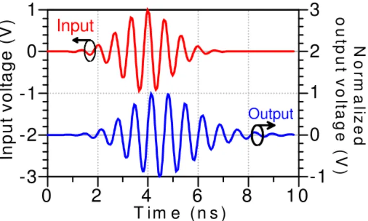
4 depicts the BER as function of the modulation index considering the transmission of two OFDM-UWB signals located in two different UWB sub-bands and for two different lengths of SSMF
This paper presents a dynamic model of a wind turbine equipped with a transverse flux permanent magnet generator connected to a direct-current power system using
