Marcin Józef
Janiszewski
Unidade de Efeitos de Áudio
Audio Effects Unit
Universidade de Aveiro Ano 2011
Departamento de Electrónica, Telecomunicações e Informática
Marcin Józef
Janiszewski
Unidade de Efeitos de Áudio
Audio Effects Unit
Układ do Generowania Efektów Dźwiękowych
Dissertation submitted to the University of Aveiro as part of its Master’s in Electronics and Telecommunications Engineering Degree. The work was carried out under the scientific supervision of Professor Telmo Reis Cunha of the Department of Electronics, Telecommunications and Informatics of the University of Aveiro.
Mr. Marcin Janiszewski is a registered student of Technical University of Lodz, Lodz, Poland and carried out his work at University of Aveiro under a joint Campus Europae program agreement. The work was followed by Professor Marcin Janicki at Technical University of Lodz as the local Campus Europae Coordinator.
o júri
presidente Professor Doutor Dinis Gomes de Magalhães dos Santos
Professor Catedrático do Departamento de Electrónica, Telecomunicações e Informática da Universidade de Aveiro
Professor Doutor Carlos Miguel Nogueira Gaspar Ribeiro
Professor Adjunto do Departamento de Engenharia Electrotécnica da Escola Superior de Tecnologia e Gestão do Instituto Politécnico de Leiria
Professor Marcin Janicki
Associate Professor of Department of Microlectronics and Computer Science of Faculty of Electrical, Electronic, Computer and Control Engineering,Technical University of Lodz, Lodz, Poland
Professor Doutor Telmo Reis Cunha
Professor Auxiliar do Departamento de Electrónica, Telecomunicações e Informática da Universidade de Aveiro
palavras-chave
processamento de sinais audio, microcontroladores, conversão analógico-digital e analógico-digital-analógico, desenvolvimento de circuitos impressos, conexão USB.
resumo
O objectivo principal da presente tese de mestrado centrou-se no desenho e construção de uma unidade de efeitos de áudio (Audio Effects Unit -AEU), cuja função consiste em processar sinais áudio em tempo real. O propósito central foi desenvolver uma unidade de processamento áudio genérica, cuja função de processamento, implementada no domínio digital, pode ser facilmente especificada pelo utilizador via uma aplicação de software implementada num computador.
A primeira etapa deste projecto consistiu na implementação completa do hardware que constitui o AEU. É importante acrescentar que esta concepção teve em conta a inclusão desse hardware numa caixa apropriada. Este método de projecto e implementação constituiu uma experiência muito interessante e útil.
A próxima etapa consistiu no desenvolvimento de algoritmos matemáticos a ser implementados no microcontrolador do AEU e que geram os efeitos sonoros desejados por processamento dos sinais áudio originais. Estes algoritmos foram inicialmente testados através do Matlab.
Para controlar os efeitos sonoros produzidos foi ainda criada uma aplicação de computador que permite a intervenção, de forma muito simples, do utilizador. A referida aplicação assegura a comunicação entre o microcontrolador do AEU e o computador através de uma ligação USB. O dispositivo, na sua versão final, foi testado em laboratório e através do Matlab. Cada bloco do dispositivo, e o dispositivo completo, foi testado individualmente. Com base nessa avaliação foram desenhadas as respectivas características na frequência e analisada a qualidade do dispositivo de áudio. Para além da experiência adquirida em concepção de hardware, este projecto permitiu-me alargar o meu conhecimento em programação de microcontroladores e na optimização de código, um requisito do processamento de sinal em tempo real. Também me deu a oportunidade de utilizar a ferramenta comercial MPLAB para programação de microcontroladores.
keywords audio signal processing, microcontrollers, analog-digital and digital-analog conversion, printed circuit boards development,USB connection.
abstract The main aim of this master thesis was to design and build an Audio Effects Unit (AEU), whose function is to process, a particular audio signal in real time. The objective was to develop a general purpose audio processing unit where the processing function, implemented in the digital domain, can be easily specified by the user by means of a software application running on a computer.
The first stage of this project consisted on the full design and implementation of the hardware that constitutes the AEU. It is worth adding that such design also considered that the layout could be placed in an enclosure. Such way of designing was a great new experience.
The next stage was to prepare the mathematical algorithms to be implemented in the AEU microcontroller which create the sound effects by processing the original audio signal. These algorithms were first tested in MatLab.
To control the produced sound effects a computer program was created which allows the user intervention in a straightforward way. This program ensures communication between the AEU microcontroller and PC software using an USB connection.
The completed device was tested in laboratory and with Matlab. The individual blocks of the AEU, and the whole device, were tested. On the basis of these tests frequency characteristics were drawn and the quality of the audio device was analyzed.
Besides acquiring expertise in hardware design, this project has broadened my knowledge on microcontroller programming and code optimization, a requirement for real time signal processing. It also gave me the opportunity to use the commercial MPLAB programming environment.
słowa kluczowe
przetwarzanie sygnału dźwiękowego, mikrokontrolery, konwersja analogowo cyfrowa i cyfrowo analogowa, budowa obwodów drukowanych, połączenie USB.
streszczenie
Głównym celem tej pracy magisterskiej było zaprojektowanie i zbudowanie układu do generowania efektów dźwiękowych (Audio Effects Unit - AEU) służącego do przetwarzania sygnału dźwiękowego w czasie rzeczywistym. Zadaniem autora było skonstruowanie ogólnego zastosowania układu przetwarzającego sygnał dźwiękowy, w którym funkcja przetwarzania, zaimplementowana w sposób cyfrowy, może być łatwo określona przez użytkownika poprzez zastosowanie odpowiedniego oprogramowania komputerowego.
Pierwszy etap projektu polegał na szczegółowym zaprojektowaniu i zbudowaniu warstwy sprzętowej tworzącej AEU. W projekcie przewidziano tez możliwość umieszczenia układu w obudowie, co było dla autora nowym doświadczeniem projektowym.
Kolejnym etapem było opracowanie algorytmów matematycznych, zaimplementowanych w mikrokontrolerze AEU, które tworzą efekty dźwiękowe poprzez przetwarzanie oryginalnego sygnału dźwiękowego. Te algorytmy zostały najpierw przetestowane w programie MatLab.
Do kontrolowania wytworzonych efektów dźwiękowych, został napisany program komputerowy, który pozwala na prostą interakcje z użytkownikiem. Ten program zapewnia komunikację między mikrokontrolerem AEU i oprogramowaniem komputerowym poprzez złącze USB.
Gotowe urządzenie zostało zbadane w laboratorium oraz za pomocą programu Matlab. Poszczególne bloki AEU jak i całe urządzenie zostały przetestowane, co pozwoliło na wykreślenie charakterystyk częstotliwościowych i umożliwiło analizę jakości wykonanego urządzenia audio.
Oprócz zdobywania doświadczenia w projektowaniu sprzętu, udział w projekcie poszerzył moją wiedzę o programowaniu mikrokontrolerów i optymalizacji kodu, potrzebną dla przetwarzania sygnału w czasie rzeczywistym. Ponadto miałem możliwość zapoznania się z komercyjnym środowiskiem programistycznym MPLAB.
I
Table of contents
Table of contest ... I List of Figures ... III List of Tables ... V
Chapter I: Introduction and Objectives ... 1
Chapter II: State-of-the-art Survey ... 5
II.1. Properties of audio signals ... 5
II.2. Typical architecture of digital processing units for audio signals ... 8
II.2.1. Digital Signal Processing Units ... 9
II.2.2. Analog to Digital Converters ... 13
II.2.3. Digital to Analog Converter/ DAC ... 18
II.3. The usual communication protocol between Microcontroller and ADC/DAC ... 20
II.3.1. I2S ... 21
II.3.2. I2C ... 23
II.3.3. SPI ... 25
II.4. Signal conditioning of input and output channels of audio devices ... 28
II.5. Audio effects... 29
Chapter III: Description of the Designed Part of the Work ... 35
III.1 PIC32 Module Design ... 35
III.1.1. Choice of microprocessor (why the PIC32MX795F512H)... 35
III.1.2. Schematics ... 36
III.1.3. PCB ... 38
III.2 Audio Effects Unit Design ... 39
III.2.1. General Architecture ... 39
III.2.2. Choice of Components ... 39
III.2.3. Schematics ... 41
III.2.4. PCB ... 45
III.2.5. Final Assembly ... 47
Chapter IV: Audio Effects Algorithms ... 49
IV.1. Equalization effect ... 49
II
IV.3. Chorus ... 54
IV.4. Distortion ... 56
Chapter V: Software Design ... 57
V.1. PIC32 Module Firmware ... 57
V.2. PC Software for AEU Effects Generation ... 60
Chapter VI: Audio Effects Unit testing ... 63
Chapter VII: Conclusions and Future Work ... 69
III
List of Figures
Figure 1 - General AEU implementation diagram. ... 2
Figure 2 Audio signal in: a) time domain b) frequency domain. ... 5
Figure 3 Main classification of sound waves according to their frequency. ... 6
Figure 4 Bit resolution and frequencies (in kHz) in Audio common audio devices. ... 8
Figure 5 Typical architecture of a real-time audio signal processing device... 9
Figure 6 Harvard architecture. ... 10
Figure 7 N-bit Two-Stage Sub-ranging ADC. ... 14
Figure 8 Basic Pipelined ADC with Identical Stages: a) k-bits per stage b) 1-bit per stage. ... 15
Figure 9 Example of operation in Pipelined ADCs... 15
Figure 10 Successive Approximation ADC Block Diagram. ... 16
Figure 11 Capacitive Binary-Weighted DAC in Successive Approximation ADC. ... 17
Figure 12 First order single and multibit Sigma-Delta ADC block diagram. ... 18
Figure 13 Voltage-mode Binary-Weighted Resistor DAC. ... 19
Figure 14 Segmented Unbuffered String DACs. ... 19
Figure 15 Delat Sigma DAC. ... 20
Figure 16 I2S system configuration. ... 22
Figure 17 Recommended connection for I2C. ... 23
Figure 18 I2C connection between 6 devices. ... 24
Figure 19 A complete data transfer with START and STOP conditions in a I2C bus. ... 25
Figure 20 Multiple slave SPI implementation example. ... 25
Figure 21 SPI transmit and receive mechanism. ... 26
Figure 22 Typical SPI timing in sending information. ... 27
Figure 23 Way of propagation waves in a closed room. ... 30
Figure 24 Soft and hard clipping. ... 31
Figure 25 Asymmetrical soft clipping. ... 32
Figure 26 WahWah effect illustration. ... 33
Figure 27 Series connection of two shelving and two peak filters. ... 34
Figure 28 Schematic of PIC32 Module. ... 37
Figure 29 Audio Effects Unit block diagram. ... 39
Figure 30 Frequency response, fcutoff=8/32/128 kHz. ... 40
Figure 31 First Audio Effects Unit Schematics. ... 43
Figure 32 Connection between PIC32 Module and Audio Effects Unit. ... 44
Figure 33 Corrected Audio Effects Unit Schematics. ... 46
Figure 34 Executing circuit of AEU. ... 48
Figure 35 Final appearance of AEU. ... 48
IV
Figure 37 Amplitude spectrum for -6dB and 6dB. ... 52
Figure 38 Delay effect algorithm block diagram... 53
Figure 39 Result of delay algorithm. ... 54
Figure 40 Chorus effect algorithm block diagram. ... 54
Figure 41 Result of chorus algorithm. ... 55
Figure 42 Result of distortion effect. ... 56
Figure 43 PIC32 Module firmware flowchart. ... 58
Figure 44 Main Window. ... 61
Figure 45 Equalizer Window and Delay Window. ... 61
Figure 46 Chorus Window and Distortion Window. ... 62
Figure 47 Results after operational amplifier stage with 1 kHz signal. ... 63
Figure 48 Frequency characteristic of input active filter. ... 64
Figure 49 Frequency characteristic of output active filter. ... 64
Figure 50 Input vs. output in time and amplitude domains. ... 65
V
List of Tables
Table 1 Frequency of the musical single tones. ... 7
Table 2 A selection of commercially available DSPs. ... 11
Table 3 DSC Devices from the three different vendors... 12
Table 4 General comparison between SPI and I2C protocols. ... 27
Table 5 Shelving filter design's equations. ... 510
1
Chapter I:
Introduction and Objectives
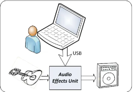
Signal processing for audio applications has been a topic of thorough research in the last decades, generating several solutions at different levels of the audio field. A search through the commercially available audio equipment reveals the existence of several devices whose purpose is to process, or transform, an input audio signal into another audio signal with added properties. Examples are amplifiers, filters, equalizers and audio effects devices. A particular class of audio devices is dedicated to transform the signals that are produced by musical instruments, giving them more flexibility in terms of the variety of sound characteristics they can produce. A typical example is that of the electric guitar which whose generalized use throughout most of the spectrum of musical genders was only made possible by the audio processing devices that process the electrical signal it generates. Traditionally, these processing devices are based on analog implementations, but in recent years, with the development of digital technology, digital processing units are proving to be very competitive with the former analog solutions. There seems to be a tendency for every analog circuit to be realized through a digital system. This can be justified by the extra flexibility that digital processing has over analog solutions, since the very same hardware can be used to process the audio signals in many different ways, just by changing the digital algorithm that performs such processing.
With this in mind, the work here presented consists on the development of a digital-based electronic device whose objective is to process the electric signal generated by a musical instrument (in fact, it may be generated by any device that produces voltage signals in the audio frequency range), and to send out the transformed voltage signal so that it can be amplified by an audio amplifier, or captured by an audio sampling system. Even though this device, denominated Audio Effects Unit (or simply, AEU), was more focused on processing
Audio Effects Unit
2
algorithms commonly used to create sound effects for electric guitars, it can be used with any other audio signal source that makes available the source signals as a voltage wave. Even though there can be found in the market several audio devices which can generate a specified set of sound effects, the idea behind this work was to develop a sound processing device whose processing algorithm could be designed by the user, in a computer, and uploaded into the device. This way, the number of sound effects that can be produced by the developed device is limited only by the imaginative ability of the user.
Moreover, this work had also as objectives to allow the acquisition of knowledge and practice in different, but important, fields of electrical engineering, such as: analog circuit design, digital circuit design, PCB design and elaboration, device design, digital signal processing, USB and I2C communication, among others.
The basic diagram for the AEU implementation is depicted in Figure 1. As shown, the signal generated by the musical instrument is processed by the AEU, which sends the transformed signal directly to the audio amplifier. By means of an USB2.0 connection, the user can specify and upload into de AEU the algorithm that performs the AEU signal processing. Preceding the design stage of the AEU, a set of basic requirements was specified for the AEU, which include:
Guaranteeing a good quality of the output audio signal;
Good linearity characteristics (i.e., low undesirable distortion);
Low noise addition.
3
To design and upload the AEU processing algorithms, a user-friendly MS-Windows based application is to be developed, providing the user with different examples on how to perform this task. Among other objectives, this interface (and the ability that the AEU has to be programmed in such an easy manner) allows the user to test the impact that variation of the algorithm parameters has on the produced sound effects.
To provide the user with more flexible sounds, the commercially available sound processing devices usually allow different effects to be simultaneously active (on moderate cost devices, the number of simultaneous effect is usually three). Thus, it was established as an additional requirement that the developed AEU allows the simultaneous use of four independent effects, being set active (or deselected) by the user by means of buttons placed on top of the AEU device. If active, these effects are executed, in series, by the digital processing unit of the AEU.
Besides the hardware design and respective implementation, this project involves the challenging task of on-the-fly processing the audio samples in a very efficient way so that information is not lost. To maintain a high level of audio signal quality it is required to have simultaneously a high sampling rate and a high resolution of the analog to digital conversion. Thus, the processing algorithms which transform the original audio signals into those enhanced with sound effects must be carefully controlled in terms of computational efficiency since, with common microcontrollers, the time available to process will impose a significant restriction.
5
Chapter II:
State-of-the-art Survey
II.1. Properties of audio signals
Sound (acoustic wave) is a mechanical wave that is an oscillation of pressure. It can be transmitted through a solid, liquid or gas medium. This third propagation medium is most common for our ears. Sound, as heard by humans, is composed of frequencies on the approximate range of 20 Hz to 20 kHz [Kahr 4], with a level sufficiently strong to be heard, as we can see in Figure 2. Even though most authors define the lower limit of the audio frequency as 20 Hz, there are other scientific manuscripts that state that it is 16 Hz [Body 285].
Audio Effects Unit
6
Sound waves are classified in three main groups: infra sounds, audible sounds, and ultra sounds. In Figure 3 is shown the distribution of such groups in the frequency scale.
As we can see, the frequencies of audible sound lie within the 20 Hz to 20 kHz range. This range is, naturally, just an indication, because not every human ear can hear through all of this range. Some people can only hear part of this range. Also, when we grow old our capability to hear becomes diminished.
Figure 3 Main classification of sound waves according to their frequency.
Vibrations from 20 to 300 Hz are known as low frequencies and from 3 kHz to 20 kHz as high frequencies. Human ear is most sensitive for frequencies in range of 300– 3000Hz.
Even though the audio effects device developed in this work can be intended for general purpose audio, thus processing signals generated from distinct equipment, its common application is to modify the properties of sound waves produced by musical instruments. One of the most common uses is to process the electric analog signal generated by the pick-ups of a guitar instrument. So, the characteristics of these signals need also to be analyzed in the scope of the development of the audio effects device.
For the case of a typical guitar instrument (and also of others musical instruments), the range of generated frequencies is narrower than the full audio range. In Table 1 [Proj] are shown the musical tones and theirs corresponding frequencies (the frequencies for the six unconstrained cords of a standard guitar are highlighted in red). The highest string has generates a 330 Hz tone if freely played, but it can go as high as its fourth harmonics, yielding a maximum frequency of 1320 Hz.
7 Frequencies [Hz] Name
of octave
Typical name for tones
Typical designation for voices C C# D D# E F F# G G# A A# B 1st 16.4 17.3 18.4 19.4 20.6 21.8 23.1 24.5 26.0 27.5 29.1 30.9 C2 2nd 32.7 34.6 36.7 38.9 41.2 43.7 46.2 49 51.0 55.0 58.3 61.7 C1 3th 65.4 69.3 73.4 77.8 82.4 87.3 92.5 98.0 103.8 110.0 116.5 123.5 C 4th 130.8 138.6 146.8 155.6 164.8 174.6 185.0 196.0 207.7 220.0 233.1 246.9 c 5th 261.6 277.2 293.7 311.1 329.6 349.2 370.0 392.0 415.3 440.0 466.2 493.9 c1 6th 523.3 554.4 587.3 622.3 659.3 698.5 740.0 784.0 830.6 880.0 932.3 987.8 c2 7th 1046.5 1108.7 1174.7 1244.5 1318.5 1396.9 1480.0 1568.0 1661.2 1760.0 1864.7 1975.5 c3 8th 2093.0 2217.5 2349.3 2489.0 2637.0 2793.8 2960.0 3136.0 3322.4 3520.0 3729.3 3951.1 c4 9th 4186.0 4434.9 4698.6 4978.0 5274.0 5587.7 5919.9 6271.9 6644.9 7040.0 7458.6 7902.1 c5 10th 8372.0 8869.8 9397.3 9956.1 10548.1 11175.3 11839.8 12543.9 13289.8 14080.0 14917.2 15804.3 c6
Table 1 Frequency of the musical single tones.
The Nyquist-Shannon theorem defines the sampling frequency limit in a sampling process. It is known that if we want to precisely reconstruct a continuous signal from discrete one, without losing any information from the continuous signal that initially originated the sampled signal, then the considered sampling frequency must be higher than at least two times the highest frequency within the original signal. So, for a general audio signal, the sampling frequency must be higher than 40 kHz, otherwise aliasing-effects will occurs. However, if the limit is imposed by the musical instrument that generates the audio signal to be processed, then the sampling frequency can be significantly reduced (for instance, a frequency of 2640 Hz would be the lower limit for sampling the signals generated by a guitar instrument).
In Figure 4 is shown the usual sampling frequencies (given in kHz), and also the respective bit resolution, used in audio applications.
Audio Effects Unit
8
Figure 4 Bit resolution and frequencies (in kHz) in Audio common audio devices.
II.2. Typical architecture of digital processing units for audio
signals
The typical topology used in real-time signal processing units for audio applications is depicted in Figure 5. The main block, in the middle, consists on a digital processing unit (such as a micro-processor or micro-controller) which receives the digital samples of the input audio signal, generated by an analog-to-digital converter (ADC), and processes them according to specific algorithms. These algorithms change the sampled input signal according to the device objectives – for instance, this can be a simple filter, an equalizer, or, as is the case in the work here presented, it can add effects to the original audio signal such as echo, reverb, distortion, or others commonly encountered in commercial devices.
The modified samples are then sent by the processing unit to a digital-to-analog converter (DAC). Since the conversion from analog domain to the digital domain introduces quantization error, a low-pass filter is usually used to interface the DAC output with the device output. Moreover, DC level adjustment and signal amplitude amplification is usually also necessary at this point. These filtering and signal adjustment operations are included in the block generally denominated as output signal conditioning block.
9
Also common in real-time signal processing devices is the input signal conditioning which, again, filters the input signal (usually to eliminate higher frequency noise) and adjusts the DC and amplitude levels to the specifications of the ADC input.
Figure 5 Typical architecture of a real-time audio signal processing device.
II.2.1. Digital Signal Processing Units
Digital signal processing units present several advantages over those based on analog signal processing. The most significant of these is that microprocessor systems are able to accomplish tasks inexpensively that would be difficult or even impossible using analog electronics. Digital systems are also insensitivity to environment changes. For example, analog circuits’ behavior depends on its temperature, while digital system delivers the same response independently of the temperature (naturally, within the device’s safe range of operation). Additionally, they are almost insensitive to component tolerances. They are also reprogrammable, which makes them useful not only for one concrete functionality but for a large number of applications (maintaining the same hardware). Another advantage of the use of microprocessors is the size reduction of devices, when compared with analog ones. In fact, as the microprocessor concentrates in a single (small) chip the input-output behavior of the signal processing system, it avoids the necessity of using a considerable number of discrete components which would be necessary to be considered in an analog implementation. However, there are also important disadvantages associated with microprocessors such as finite memory and limited processing time. This last issue is of high importance, being many times the bottleneck of many applications. In fact, as the microprocessor operates in a clocked way, processing every program instruction in a step-by-step mechanism, the number of instructions that are possible to be executed between two consecutive samples acquired by the external ADC is limited. Moreover, this limitation is further restricted as the sampling frequency increases, limiting the flexibility of the processing algorithm.
Audio Effects Unit
10 Digital Signal Processors
Microcontrollers
Digital Signal Controllers
All of them are implemented according to the Harvard architecture (shown in Figure 6), which makes use of separate program and data memories.
Figure 6 Harvard architecture.
The first group is Digital Signal Processors (DSP), sometimes called also Programmable Digital Signal Processors (PDSP). These are microprocessors that are specialized to achieve high performance in digital signal processing-intensive applications. DSPs are sometimes found in applications requiring high frequency operation like: Radio Signaling and Radar, High Definition Television, Video [Phil 4] etc. Usually their clock rates can be up to 100 MHz for common use, with faster rates can be found in some high-performance products [Phil 5]. Hardly ever, they are used in low frequency systems, such as: Seismic Modeling, Financial Modeling and Weather Modeling. In this three modeling systems, algorithms are complex and microprocessor need time to execute functions. It is possible to say that, if quantity of sample rate is growing, algorithm complexity is decreasing.
In audio applications it is common to use DSPs to implemented specific functionalities, like: speech synthesis, Hi-fi audio encoding and decoding, noise cancellation, audio equalization, sound synthesis and more.
The DSP market is very large and growing rapidly. According to the market research, sales of user-programmable DSPs in 1996 were about two billion dollars and in 2002 were around sixteen billion dollars. In Table 2 [Phil 10], are shown the most common DSP processors.
11
Vendor Processor Family
Data Width Analog Devices ADSP-2Ixx 16
ADSP-210xx 32 AT&T DSP16xx 16 DSP32xx 32 Motorola DSP56xxx 16 DSP563xx 24 DSP96002 32 Texas Instruments TMS320Clx 16 TMS320C2x 16 TMS320C3x 32 TMS320C8x 8|16
Table 2 A selection of commercially available DSPs.
There are a lot of advantages in using DSPs. They are adapted for working with high frequency signals and for complex algorithms. Second feature is the ability to complete several accesses to memory in a single instruction cycle. This allows microprocessor to fetch simultaneously instruction, operand and write to memory.
One disadvantage of DSPs is that they usually have a small number of peripheral circuits included. They have memory, and sometimes in expensive versions, ADCs and DACs.
The second group of microprocessors here considered is that of microcontrollers. Microcontrollers can be considered as self-contained systems with processor, memories and embedded peripherals so that, in many cases, all that is needed to use them is to add software. They include one or more timers, an interrupt controller, and last but definitely not least general purpose I/O pins. They have been designed in particular for monitoring and/or control tasks [Gunt 7]. Microcontrollers also include bit operations which allow changing one bit within a byte without changing the other bits.
Following is a list of microcontroller manufacturers, and a selection of respective microcontroller series:
Atmel (ATtiny, ATmega, ATxmega, AVR,AT91SAM )
Intel (MCS-48, MCS-51, MCS-96)
Microchip (PIC10, PIC12, PIC16, PIC18, PIC24, PIC32)
NXP Semiconductors (80C51, ARM7, ARM9, ARM Cortex-Mx )
STMicroelectronics (STM32, STM8, ST10 )
Texas Instruments (TMS370, MSP430, TMS320F28xx)
Audio Effects Unit
12 In microcontrollers are available peripherals like:
USB 2.0-compliant full-speed device
CAN module
UART modules
SPI modules
I2C™ modules
Parallel Master and Slave Port
Timers/Counters
Compare/PWM outputs
External interrupt
I/O pins
The last group of microprocessors considered is Digital Signal Controller (DSC). These are built on a single chip that incorporates features of microcontrollers and DSPs. By combining the processing power of DSPs with the programming simplicity of a microcontroller, DSCs can provide high speed and high flexibility at low costs A further advantage is that there are relatively easy to program in programming language like C or Assembly. They include many peripherals (not as many as microcontrollers). A selection of DSC commercial devices is presented in Table 3. Vendor Device Clock Speed Flash (kB) PWM MHz channels Microchip dsPIC30F 30 6-144 4-8 dsPIC33F 40 12-256 8 Texas Instruments TMS320F280x 60-100 32-256 16 TMS320LF240x 40 16-64 7-16 Freescale MC56F83x 60 48-280 12 MC56F80x 32 12-64 5-6 MC56F81x 40 40-572 12
Table 3 DSC Devices from the three different vendors.
There are also dedicated chips for audio purposes, like the TMS320C672x [Tex 3], which are characterized by a particular architecture. They have implemented three multichannel audio serial ports and operations, which make them ready for working with stereo audio signals. For communication with external devices, these are prepared with two SPI serial
13
ports, and two inter-integrated circuit (I2C) ports. For additional memory (if necessary, because internal size is about 256K-byte for RAM, and 384K-byte for ROM) it is used an external memory interface for a 100MHz SDRAM (16- or 32-bit). They are also equipped with real-time interrupt counter/watchdog.
II.2.2. Analog to Digital Converters
Analog to Digital Converters are devices which are used to convert analog signals to an equivalent digital form. In electronic literature these are usually referred by their abbreviation: ADC or A/D converter (sometimes only A/D). Since the ADC handles both analog and digital signals, its internal hardware is divided in two parts. In the analog part, the input voltage signal (which is referred to the VSS analog ground reference) is sampled by a sample-and-hold block. This sample-and-hold is controlled by a clock signal that dictates when each sample must be taken – that is, it imposes the sampling frequency. Each sampled voltage value is then converted to the digital domain by a specific mechanism (which usually requires a reference voltage VREF for such conversion). The digital samples are then ready to be sent to the controlling device (usually, a microprocessor) by means of different communication protocols (parallel or series – such as I2C, I2S, and others).
The history of first A/D converters begins at the middle of the twentieth century. The first one was called “Flash ADC” whose construction was very simple. It contains only a voltage divider (made of resistors), comparators and a decoding circuit (made from transistors). The advantage of this solution is its ultra-low conversion time. On the other side, there is the severe disadvantage that the number of required comparators raises dramatically with the bit resolution. In fact, the number of resistors (for the voltage divider) and comparators is 2N-1 for each, where N is the number of bits of the ADC. Moreover, the number of required transistors (in the decoding block) is
2
2N
N
. Nowadays, Flash converters are built for a maximum 5 - 6 bit resolution.
Generally, in high quality audio application it is needed to have a 16 bit resolution or more, and a reasonably fast speed of conversion. There are three main groups of ADCs, which are suited for these requirements: Sub-ranging especially with Pipeline architecture; Successive approximation; and Sigma-Delta.
Audio Effects Unit
14
Figure 7 N-bit Two-Stage Sub-ranging ADC.
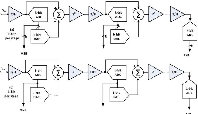
The input is first converted by an N-bit A/D converter (it can be used a Flash ADC when N is small enough), resulting on the N most significant bits (MSB) of the output register. Then, such digital value is converted back into analog format by an N-bit DAC and subtracted from the input, this gives a residue for next stage. Afterwards, with an appropriate gain operator, the residual analog signal is again converted by another ADC with the same resolution (N). This produces the least significant bits (LSBs) of the output register, forming a complete 2N resolution conversion. Although this description considered only a two-stage conversion, more stages can be considered (which, for the same final resolution, requires an ADC at each step with lower resolution N).
The pipelined architecture allows the previous stage to process the next sample at the same time that the current stage is still processing the current sample. At the end of each phase of a particular clock cycle, the output of a given stage is passed on to the next stage using the T/H (Track and Hold) functions and new data is shifted into the stage.
This method is shown in Figure 8 [Wal 71], where converters with identical stage are presented. There is also the possibility to combine non-identical stages, which is required in odd resolution converters.
The effect of “pipeline delay” in the output is shown in Figure 9 [Wal 69]. Delay is a function of the number of stages and blocks. Advantage of this architecture is that in one time are converted more than one samples of the signal, which makes these converters really high speed. For example, the 12-bit AD9235 (from Analog Devices) has efficiency up to 65 Mega Samples per Second (MSPS).
15
Figure 8 Basic Pipelined ADC with Identical Stages: a) k-bits per stage b) 1-bit per stage.
CLOCK INPUT T H T H T H T H T STAGE 1 H T H T H T H T H STAGE 2 T H T H T H T H T STAGE 3 H T H T H T H T H FLASH T H T H T H T H T
DATA OUT DATA OUT DATA OUT DATA OUT
Figure 9 Example of operation in Pipelined ADCs.
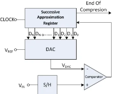
The second group of ADCs here considered is the Successive Approximation ADC, sometimes called SAR ADC. The operation principle is shown in Figure 10 [Wal 54].
Audio Effects Unit
16
Figure 10 Successive Approximation ADC Block Diagram.
This device makes use of the successive approximations algorithm. The idea is simple. Firstly, the input signal passes through the Sample-and-Hold (S/H) block, where it is sampled and latched. For better explanation, let us analyze a particular example where VIN= 43 V, VREF= 32 V and N=5 (6 bit conversion). Firstly, SAR sets the MSB and input of the DAC is:
D543210=100000 VDAC= 32 VCOMP=1, because VIN> VREF and this value is latched in SAR
register as D5, and the next bit is then set to “1”,
D543210=110000 VDAC= 32+16=48 VCOMP=0 and this value is latched as D4,
D543210=101000 VDAC= 32+8=40 VCOMP=1 and D3=1,
D543210=101100 VDAC= 32+8+4=44 VCOMP=0 and D2=0,
D543210=101010 VDAC= 32+8+2=42 VCOMP=1 and D1=1,
D543210=101011 VDAC= 32+8+2+1=43 VCOMP=1 and D0=1.
After conversion SAR sets a signal EOC (End of Compression) and the output of this register is the final result, which in this situation is 4310 = 1010112.
In successive approximation ADCs, most often Binary-Weighted DACs, are used, which are described in Section 2.2.3. Nowadays for this solution, manufacturers produce Capacity Binary-Weighted DACs, whose architecture is shown in Figure 11 [Wal 56]. The main reason
17
for using capacitors instead of resistors is the possibility of making smaller Integrated Circuits.
Figure 11 Capacitive Binary-Weighted DAC in Successive Approximation ADC.
The third group is Delta Sigma converters, which sometimes are called over sampling converters. Sigma-delta converters, which are shown in Figure 12[Wal 111], consist of 3 major blocks: modulator, digital filter and decimator. The modulator includes an integrator and a comparator (or N-bit flash ADC) with a feedback loop that contains a 1-bit (or N-bit) DAC. The modulator is oversampling the input signal, transforming it to a serial bit stream with a frequency K times above the required sampling rate. The output digital filter reduces bandwidth and then decimator converts the bit stream to a sequence of parallel digital words at the sampling rate. Decimation does not cause any loss of information.
Biggest advantages of them are high resolution (up to 24 bit) and low cost. Even if key concepts are easy to understand, mathematical calculation is complex. The penalty paid for the high resolution achievable with sigma-delta technology has always been speed. These converters have traditionally been used in high-resolution low frequency applications (such as speech, audio, precise voltage and temperature measurements).
Another advantage of these converters is that they shape the quantization noise, so that most of it falls outside digital filter pass band. When number of order sigma delta converter is rising, SNR is also rising. Number of sigma-delta blocks, defines order of converter.
Audio Effects Unit
18
Figure 12 First order single and multibit Sigma-Delta ADC block diagram.
II.2.3. Digital to Analog Converter/ DAC
The simplest DAC structure of all is the divider or string DAC [Wal 4]. An N-bit version of this DAC simply consists of 2N equal resistors in series (they are located between VREF and VSS) and 2N switches (usually CMOS), one between each node of the chain and the output. The output is taken from the appropriate tap by closing just one of the switches. Relation between N-bit digital value and chosen switch bases on principle of operation N to 2N decoder.
Exponential growing number of required resistors and switches, in this type of DAC, is big disadvantage for higher N-bit resolution. It is possible to say that evolution of them was binary-weighted DACs. They need only N resistors and N switches, as it is shown in Figure 13 [Wal 10]. Change of switch position, supply resistor adequately VREF or ground for corresponding resistor. Values of resistors are successive power of two. To MSB is connected resistor with highest value. Output voltage is a sum of particular resistors.
19
Figure 13 Voltage-mode Binary-Weighted Resistor DAC.
Binary–weight resistor DAC can be manufacture in current-mode. There is another modification of this type DACs structure, which has recently become widely used. It is Capacitive Binary-Weighted DAC, which is shown in Figure 11.
Another group D/A converters are segmented DACs. They consist of two or more String DAC. This solution gives possibility to obtain required performance. In Figure 14 is presented 6-bit segmented DAC composed of two 3-bit string DACs. To understand this clever concept better the actual voltages at each of the taps has been labeled.
Figure 14 Segmented Unbuffered String DACs.
The resistors in the two strings must be equal. One resistor placed at the top first String DAC must be smaller—1/2K of the value of the others. Number of resistor responsible for MSBs must be equal 2N, but number of resistors responsible for LSBs is equal 2N-1. At two extreme points of second String DAC occurs voltage taken from output of first. Output signal is taken from adequate resistor.
Audio Effects Unit
20
Sigma-Delta DAC is a next presented group of D/A converters. In Figure 15 [Wal 133] is shown theirs block diagram. It consists of four blocks. First, interpolation filter is a digital circuit which accepts data at a low rate, inserts zeros at a high rate. Then it applies a digital filter algorithm and at output occurs high rate data. After is a digital Sigma-Delta modulator, which effectively works as a low pass filter to the signal but as a high pass filter to the quantization noise. Third block is an M-bit DAC, which convert digital stream to 2M analog levels. After that output is filtered in an analog low pass filter to remove high frequency noises, which come from digital part of device.
Figure 15 Delat Sigma DAC.
II.3. The usual communication protocol between Microcontroller
and ADC/DAC
There are two possibilities of data transmission between microcontrollers and ADCs or DACs:
Serial transmission –bits are sent sequentially, one bit after another, in one channel (wire). This makes it really cheap in design, but on the other hand it is a slow process.
Parallel transmission – bits are sent simultaneously on different channels (wires). This makes this a fast process, but designing is expensive.
There are two types of serial transmission: synchronous and asynchronous. In this first one, groups of bits are combined into frames and frames are sent continuously. In the second one, groups of bits are sent as independent units with start/stop flags. There is no synchronization. In both groups sometimes between frames are sent bits of acknowledgment.
21
In audio signal systems, in serial synchronous transmission, there are three main standards:
I2S
I2C
SPI
II.3.1. I2S
This is a standardized communication structure for exchanging information between two digital devices. Inter-IC sound (I2S) bus is a serial link especially for digital audio. It is used in Audio Signal Microprocessors, Analog-to-Digital converters, and Digital-to-Analog converters. They are also used in professional audio applications like: mixers, effects boxes, audio synthesis, audio conferencing, [I2S 1] etc. This standard is compatibility with stereo signals.
To minimize the number of pins required and to keep wiring simple, a 3-line serial bus is used consisting of a line for two time-multiplexed data channels, a word select line and a clock line.
The I2S protocol allows different connection configurations between devices. Figure 16 presents some examples of such configurations.
The I2S specification considers 3 lines [I2S 2]:
continuous serial clock (SCK)
word select (WS) - indicates which channel is being transmitted: - WS = 0; channel 1 (left)
- WS = 1; channel 2 (right)
Audio Effects Unit
22 .
Figure 16 I2S system configuration.
When the transmitter and receiver have the same clock signal for data transmission, and if transmitter is the master, the latter has to generate the bit clock, word-select signal and data. But if the receiver is the master, it has to generate only the bit clock and the word-select.
In complex systems, where there may be several transmitters and receivers, it is difficult to define the master. In such systems, there is usually a system master controlling the digital audio data-flow between the various ICs. It generates only SCK and SD.
Serial data is transmitted in two data frames, one for left channel and one for right channel, which each one of them starts with MSB. MSB is transmitted first because the transmitter and receiver may have different word lengths. It is not necessary for the transmitter to know how many bits the receiver can handle, nor does the receiver need to know how many bits are being transmitted.
In that situation, when word length is not the same:
- transmitter sends more bits than receiver can handle, bits after LSB are ignored - transmitter sends less bits than receiver needs, this needed bits are padded with ‘0’
For being sure that the most important bits are sent and received, the transmitter always sends the MSB of the next word one clock period after the WS changes.
23
Serial data sent by the transmitter may be synchronized with either the trailing (HIGH-to-LOW) or the leading (LOW-to-HIGH) edge of the clock signal. However, the serial data must be latched into the receiver on the leading edge of the serial clock signal.
II.3.2. I2C
This specification for data transmission needs only two wires: - SDA; serial data
- SCL; serial clock
Both SDA and SCL are bi-directional lines, connected to a positive supply voltage via a current-source or pull-up resistor. When the bus is free, both lines are HIGH. The output stages of devices connected to the bus must have an open-drain or open-collector to perform the wired-AND function. A typical connection is shown in Figure 17 [I2C 8].
Figure 17 Recommended connection for I2C.
Like in I2S, in I2C there are also the distinct concepts of: transmitter, receiver, master and slave. There are also more two important definitions: multi-master and arbitration [I2C 7]. The first means that the bus can be controlled by different devices at different times. The second means that if more than one master tries to control the bus, only one is allowed to do that
Audio Effects Unit
24
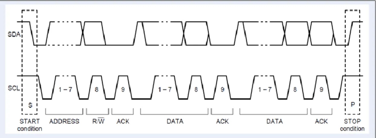
.Messages, which were not serviced, are waiting to control the bus. In Figure 18 is shown an example where more than one master are present.
Figure 18 I2C connection between 6 devices.
Another difference between I2S and I2C is that in the second one we can have more than one receiver and more than one transmitter. But this generates a problem. Which device will be transmitting and which will be receiving at a particular moment?
Each device is recognized by a unique address. When the master (in this case, a microcontroller) starts a session, it sends on the bus the address of the device which will be working in accordance with its purpose. As we can see in Figure 19 [I2C 10], after this address, it sends a bit R/(~W) which indicates that master will be writing on reading. The ninth bite is an acknowledgment.
25
Figure 19 A complete data transfer with START and STOP conditions in a I2C bus. II.3.3. SPI
This standard needs 4 wires [Ser 3]: - SCK – Continuous clock
- SI – Data input - SO – Data output
- CS – Chip select (active low)
It is possible to divide this line into two groups: control lines (SCK, CS) and data lines (SI, SO). In Figure 20 is shown an example of a possible configuration with 1 master and 2 slaves.
Audio Effects Unit
26
The master decides with which peripheral device it wants to communicate. In this simple way a system can be organized with several slave devices. Another difference between I2C and SPI is that the SPI bus does not need any external pull-up resistors.
In Figure 21 [Pic 23] is shown typical SPI transmit/receive mechanism. As we can see, at one time instant, a device can only get or send information. Reading and writing services use corresponding for them buffers.
The sizes of buffers are usually: 8 / 16 / 32 bits. If our data resolution is between these three values, we always choose the next higher value. We have also the possibility to decide on what edge of clock signal data will be transmitted.
A pair of parameters, called clock polarity (CKP) and clock edge (CPHA), determines the edges of the clock signal on which the data are driven and sampled. Each of the two parameters has two possible states, which allows for four possible combinations, all of which are incompatible with one another. So a master/slave pair must use the same parameter pair values to communicate. These are shown in Figure 22.
27
Figure 22 Typical SPI timing in sending information.
SPI
I
2C
Three bus lines are required: -SCK
-SI -SO
for more devices is also need : CS
Two bus lines are required: -SDA
-SCL
No official specification (created by
Motorola, but every device can have his own specification)
Official specification (I2C was created by Philips Semiconductor)
Higher data rates (even up to 10MHz) Lower data rates (400kHz) Efficient in configuration: single master and
single slave
Efficient in configuration: multi-masters and multi-slaves
Master is not using address to connect with device
Master is using address to connect with a specific device
Does not have an acknowledgement mechanism to confirm data reception
Has an acknowledgement mechanism to confirm data reception
Audio Effects Unit
28
In Table 4 [Ser 11] is presented a comparison between the SPI and I2C communication protocols. Contrary to I2S, which is very specific to audio dedicated devices, these two protocols are the most commonly encountered in microcontrollers and peripheral devices (as ADCs and DACs).
II.4. Signal conditioning of input and output channels of audio
devices
Conditioning systems prepare an analog signal in such a way that it meets the requirements of the next stage for further processing. They normally consist of electronic circuits performing functions like: amplification, level shifting, filtering, impedance matching, modulation, and demodulation.
In Figure 5 in Section 2.2 it is shown where input and output signal conditioning is placed in the signal processing chain. The input signal conditioning block manipulates the input signal so that the ADC works with maximum range. The voltage waveform generated from a musical instrument of from any audio device (such as an MP3 player) has positive and negative voltage values, usually oscillating around zero Volt. Moreover, the maximum amplitude of such waveform may also vary depending on the input device. Since the ADC has a full voltage range from VSS to VDD, which is usually not centered on zero Volt, the signal conditioning block must shift the dc value of the input waveform and also perform gain adjustment to take the profit of the ADC resolution.
The output signal conditioning block ensures voltage level matching to next stage component, which can be, in audio applications, a speaker, an audio amplifier, a mixing table, or any other audio processing device. In some cases, like the one of the work described in this work, the audio signal processing unit changes the properties of the signal originated from the source (like a musical instrument) and must deliver an output signal that has the same electrical characteristics of the input signal (same voltage range, same dc value). Is this case, the output signal conditioning block implements the reverse operations from those of the input signal conditioning block.
The input and output signal conditioning blocks should also filter the frequency components of the signals being processed which are not to be considered in the application. In audio applications, the input block should filter frequencies outside the audio range (or, if the device is specific to a musical instrument, for instance, it could have a narrower filter to limit the pass-band to that of such instrument. This will contribute to noise reduction and, consequently, to a better quality processed signal. The output signal conditioning block
29
should also implement a similar filter, especially to attenuate the quantization noise generated by the analog to digital conversion.
II.5. Audio effects
Nowadays, there are a lot of audio effects which are used in sound production. They arose from the moment of origin instruments and from the beginning of music. Some of them are for general purpose, others are destined for specific instruments. In this section, are presented only the most common audio effects encountered in audio processing devices. Delay/echo –the original audio signal is followed closely by a delayed repeat, just like an echo. The delay time can be as short as a few milliseconds or as long as several seconds. It depends where the virtual sound barrier, which reflects the audio signal, is. A delay effect can include a single echo or multiple echoes.
Multiple echoes occur, everywhere where more than one sound barrier is present. Delay also forms the basis of other effects such as chorus, reverb, flanger and phaser (flanging and phasing).
Chorus effect was designed to make a single person's voice sound like multiple voices singing the same thing. It can also be used for musical instruments. The main idea is making a soloist into a chorus. The original signal is duplicated, by adding multiple delays, which are short. This creates the effect of many sources, and each source is very slightly out of time and tune. This makes an illusion which we are thinking it is like in real life. There are some common parameters of this effect:
- The number of source, that we want to hear
- Delay between sound and its duplication , which is typically 20 to 30 milliseconds - Modulation waveform for generating time-varying delayed samples.
The delays which are added to original signal are not constant. Because they are changing, it makes the effect more real.
Flanger (or flanging) is an effect which is technically very similar to chorus. It is a mixture of the original and delayed signal. There are two differences between chorus and flanger. First concerns about speed of changing delay, which in flanger it is slower than in chorus. Second one is that delayed sample are taken form output, not form input like in chorus. It is worth to add that this effect produce a large number of notches (in frequency characteristic), which create musically related peaks, between those notches.
Audio Effects Unit
30
Phaser(or phasing) is an audio effect which takes advantage of the way sound waves interact with each other when they are out of phase. By splitting an audio signal into two signals and changing the relative phase between them, a variety of interesting sweeping effects can be created. When the signal is in phase (at 0 degrees, 360 degrees and 720 degrees) the signals reinforce, providing normal output. When the signals are out of phase (180 degrees and 540 degrees), they cancel each other. Number of producing notches is relatively small in comparison with flanger. A phaser is characterized as being harder and more pronounced than a chorus, but gentler than a flanger
Vibrato- an effect which is especially known in stringed (only with neck) and wind instruments, relies on regular pulsating change of pitch. Musicians make it by special playing technic. For instance, guitarists stop the finger on a string, and wobbled on the fingerboard, or actually moved up and down the string for a wider vibrato. Players of wind instruments generally create vibrato by modulating their air flow into the instrument. There are two main factors characterizing this effect. First is the “extent of vibrato” - the amount of pitch variation, and second is “rate of vibrato” – speed with which the pitch is varied. Reverb– short from reverberation, is an effect which simulates what happens with sound in different areas. It refers to the way sound waves reflect off various surfaces before reaching the listener's ear. The most common are: hall reverb, concert hall reverb, small room reverb, etc. There are also deviations from these, like: empty hall reverb and occupied hall reverb.
Figure 23 Way of propagation waves in a closed room.
In Figure 23 is shown how is created the reverb effect. The lines are a graphical representation of waves which are fetched up to the listener’s ears. The green one is called
31
main sound, which has the loudest level. Others (shown as blue), called lateral sounds, are weaker. When sound waves reflect off walls, they need longer time to reach the listener. With every bounce they lose energy, so become less audible.
Overdrive and distortion- these two effects are of the most common effects for electric guitars. The main idea is to compress the peaks of sound waves, and add overtones. The sound is created as fuzzy. Distortion is a little harder sound, good for rock music, while overdrive gives a more natural compression sound. In Figure 24 is shown the process of altering an audio signal called clipping. Differences come from that overdrive is formed by soft clipping, while distortion is formed by hard clipping.
Figure 24 Soft and hard clipping.
There are three general parameters to operate this effect: - Drive (Gain) controls the amount of overdrive
- Mix level – show how much is mixed original and distorted sound - Volume of distorted sound
Audio Effects Unit
32
Figure 25 Asymmetrical soft clipping.
There is the possibility to create some variations from these effects. One of them (shown in Figure 25) is to make asymmetrical overdrive. For this purpose there is another control parameter.The difference between them is that, symmetrical is smoother and less toothy, while asymmetrical has more aggressive sounding
Tremolo modulates the volume, like rapidly turning up and down the volume to give pulsating effect. In almost all situations is used for more than one musical instrument or audio channel. For example, it can be used to give the impression of one instrument to be appearing and disappearing against the background of other instruments. For example, guitarists used tremolo mixed with reverb to produce the sound typical of the 60’s and 70’s (many times denominated as surf music).
There are two common parameters in tremolo control: - Frequency with which volume is turning down and up
- Depth is the maximum and minimum level of volume variation.
Panning is the consolidation of two tremolo effects, one for the left channel, and another for the right channel (or sometimes one for one instrument and the second for another one). They are linked together and when left volume channel is high, right volume channel is low, and vice-versa. When input signal is in stereo format, the listener can feel that the sound “moves” from one side to the other.
WahWah effect was made popular by guitarists like Jimi Hendrix and Eric Clapton. It imitates human voices saying “wawa”. This effect has two parts: in the first on the speaker hears something similar to an open “a”, while in the second human ear hears something
33
between a “u” and a “w”. It is implemented by moving a peak in the frequency response up and down the frequency spectrum, as shown in Figure 26.
Figure 26 WahWah effect illustration.
Equalization – this effect gives the possibility to control tunes by shaping the audio spectrum, by enhancing some frequency bands and attenuating others. It is realized by a series connection of first or second order shelving and peak filters, which are controlled independently. Schematic representation is shown in Figure 27 [Udo 51].
Shelving filters boost and cut low and high frequency bands, with cut-off frequency fC and gain G controlling parameters, while peak filters are destined for mid frequencies, being controlled by the cut-off frequency fC, bandwidth fb and gain G. Peak filters are defined by the Q factor, which is given by
c b
f f
Audio Effects Unit
34
Figure 27 Series connection of two shelving and two peak filters.
Octave– a simple effect that generates a signal one or two octaves below or above the original signal. Some effect units are mixing the normal signal with the synthesized octave signal, which is derived from the original input signal by halving or doubling the frequency. Only in field of guitar effects there are over one hundred manufacturers of audio effects devices. Their history began at the middle of the twentieth century. They initially based their devices on the vacuum tube, but with the development of semiconductors, they moved to transistors. The first vendors were Warwick Electronics and Univox, which started to produce stompboxes, which are known as “effects pedals”. In the 1980s, these units began being digitalized, because of increased flexibility.
35
Chapter III:
Description of the Designed Part of the Work
Designed part of work can be divided into two sections. First section applies to description of PIC32 Module, which is a board included microcontroller from Microchip manufacturer, made in 32bit architecture. It includes indispensible components which are needed to start working with microcontroller. Second section is about Audio Effects Unit and shows individual schematic of each block and connection between them.
III.1 PIC32 Module Design
PIC32 Module is designed for general purpose for all students, which are interested in programming microcontrollers. From educational point of view there is no necessity to use 100 pins microcontroller, which has more peripheries. Microchip company offers easily programmed USB connection, which makes this board more universal for all fields of electronic. It will be used in Audio Effect Unit and Wireless Audio Unit Projects.
III.1.1. Choice of microprocessor (why the PIC32MX795F512H)
Microcontroller, that will be used, has to include:
Two channels SPI, one for receiving data from Analog to Digital converter, and another one for sending data to Digital to Analog converter. Length of SPI buffer must be minimum 16bit
Implemented USB 2.0 On-The-Go Peripheral with integrated physical layer. Device will be working as a host.
Audio Effects Unit
36
Possibly the highest working speed, for process audio effects algorithms.
Four external interrupts, to ensure possibility of changing effects, when device has been already programmed.
Data memory equals 17,4kB. 15kB is necessary to realize delay effect and 2,4kB for store samples, which are used in chorus effect.
Timer, with throwing interrupt, for set up sampling frequency.
There are available five 32bit Microchip microcontroller families. Only three of them perform above-mentioned brief foredesign: PIC32mx5xx, PIC32mx6xx and PIC32mx7xx. Differences between them are in number of peripherals. If prices of them are similar (which take place), it will be best to choose microcontroller with the highest number of included circuits and with the biggest size of memory. PIC32MX795F512H is most developed one.
III.1.2. Schematics
In Błąd! Nie można odnaleźć źródła odwołania. is shown schematic of PIC32 Module. Pins VDD must be supplied by voltage range of 2.3V to 3.6V, and pins VSS must be connected to (digital) ground. Main components that are used, to ensure correctly started with 32bit microcontroller:
Y1 – is an external main oscillator (OSC) which value equals 8MHz. PIC32 has single cycle multiply and hardware divide unit, which gives possibility to set up clock frequency to 80MHz. Oscillator pins are required to connect to capacitors in 22 pF to 33 pF range. (C8=22pF and C10=22pF). This value of oscillator ensures possibility of using PICkit3 Programmer.
Y2 – secondary oscillator (SOSC) is designed specifically for low-power operation with an external 32.768 kHz crystal. It can also drive Timer1 and the Real-Time Clock and Calendar (RTCC) module for Real-Time Clock (RTC) applications. Capacitors C11 and C12 have the same values - 22pF.
S1- switch is set between VSS and Master Clear Pin, which provides two specific device functions: device reset and device programming and debugging. This input is level sensitive, it requires a low level to create reset.
C6 – capacitor, which value equals 10µF, is required on the VCAP/VCORE pin, which is used to stabilize the internal voltage regulator output.
C1, C2, C3, C4 – decoupling capacitor which must be connected to all VDD pins, Typical value of them is 100nF.
C5 – decoupling capacitor which is connected to AVDD, even if the ADC module is not used.
37 Fi gu re 28 S ch e m at ic of P IC 3 2 M od u le .