Presidente: Professor Doutor Rodrigo Ferrão de Paiva Martins Arguente: Professor Doutor Vítor Manuel Grade Tavares Vogal: Professor Doutor Pedro Miguel Cândido Barquinha
Março, 2016
Diogo Luís Araújo de Lima
[Nome completo do autor]
[Nome completo do autor]
[Nome completo do autor]
[Nome completo do autor]
[Nome completo do autor]
[Nome completo do autor]
[Nome completo do autor]
Licenciado em Engenharia de Micro e Nanotecnologias
[Habilitações Académicas] [Habilitações Académicas] [Habilitações Académicas] [Habilitações Académicas] [Habilitações Académicas] [Habilitações Académicas] [Habilitações Académicas]
Sputtered Zn-Sn-O based thin-film transistors:
Optimization and circuit simulation
Dissertação para obtenção do Grau de Mestre em Engenharia de Micro e Nanotecnologias
Dissertação para obtenção do Grau de Mestre em
[Engenharia Informática]
Orientador:: Doutor Pedro Miguel Cândido Barquinha, Professor Auxiliar, Faculdade de Ciências e Tecnologia da Universidade Nova de Lisboa
Sputtered Zn-Sn-O based thin-film transistors: Optimization and circuit simulation
Sputtered Zn-Sn-O based thin-film transistors: Optimization and circuit simulation
iii
Sputtered Zn-Sn-O based thin-film transistors:
Optimization and circuit simulation
© Diogo Luís Araújo de Lima
Faculdade de Ciências e Tecnologia
Universidade Nova de Lisboa
A Faculdade de Ciências e Tecnologia e a Universidade Nova de Lisboa têm o
direito, perpétuo e sem limites geográficos, de arquivar e publicar esta
dissertação através de exemplares impressos reproduzidos em papel ou de
forma digital, ou por qualquer outro meio conhecido ou que venha a ser
inventado, e de a divulgar através de repositórios científicos e de admitir a sua
cópia e distribuição com objetivos educacionais ou de investigação, não
comerciais, desde que seja dado crédito ao autor e editor.
Sputtered Zn-Sn-O based thin-film transistors: Optimization and circuit simulation
Sputtered Zn-Sn-O based thin-film transistors: Optimization and circuit simulation
v
Acknowledgments
Esta dissertação marca o final de uma importante etapa da minha vida e é com grande orgulho e satisfação que hoje relembro todos os momentos que vivi na Faculdade de Ciências e Tecnologia da Universidade Nova de Lisboa, nas pessoas que conheci, nos desafios que enfrentei e no que todo esse percurso me tornou, em quem sou hoje. Como em todas as caminhadas, nunca as fazemos sozinhos, tenho por isso de agradecer a todos aqueles que me acompanharam e sempre me apoiaram neste período.
Gostaria de começar por agradecer ao Prof. Rodrigo Martins e à Prof.ª Dra. Elvira Fortunato por permitirem a minha integração na equipa do CENIMAT|i3N e CEMOP e o acesso aos laboratórios e equipamentos dos mesmos. As suas competências, dedicação e esforço pelo cultivo de uma mentalidade de qualidade e competitividade são determinantes para que seja possível alcançar o sucesso!
Em segundo lugar, agradecer em especial ao meu orientador Prof. Pedro Barquinha por me ter aceitado neste projeto, por todo o apoio e partilha de conhecimentos ao longo destes meses. Por todas as ideias que repartimos para que este trabalho se torna-se possível e por me ter dado a força que precisava quando os resultados não eram os melhores.
Obrigado Cristina e Ana Santa, minhas colegas de trabalho por longas horas, o vosso apoio e orientação na câmara limpa, por serem pacientes comigo e pelos minutos que esperaram para que eu pudesse terminar “aquela última” deposição. Quero ainda agradecer a todas as pessoas que, num contexto mais técnico, na análise de resultados ou na partilha de ideias me ajudaram durante todo o trabalho, esses são: Ganga Bahubalindruni, Asal Kiazadeh, Jorge Martins, Ana Rovisco, Diana Gaspar, Tiago Mateus, Ricardo Ferreira, Alexandra Gonçalves, Daniela Antunes, Daniela Salgueiro, Joana Vaz Pinto, Rita Branquinho, Sónia Pereira, Tomás Calmeiro e Hugo Águas.
A todos os meus amigos com os quais tive o prazer de conviver durantes estes últimos anos na FCT/UNL, em especial ao Emanuel, Allegra, Farto, Tiago, Farah, Bruno Fernandes, Íris, Inês Cunha, Paul, Raquel, Monchique e Rui Carreiras. Àqueles que não constem na lista por esquecimento, o meu sincero obrigado a todas as pessoas que de forma direta ou indireta me apoiaram.
Quero agradecer aos meus pais, Luís e Margarida, e ao meu irmão Pedro. Hoje sou o que sou graças a vocês, tudo aquilo que consegui devo-o a vós, sempre me apoiaram e aconselharam nas minhas decisões. Por acreditarem sempre em mim, muito obrigado.
Sputtered Zn-Sn-O based thin-film transistors: Optimization and circuit simulation
Sputtered Zn-Sn-O based thin-film transistors: Optimization and circuit simulation
vii
Abstract
The development of amorphous oxide semiconductors (AOS) has been accelerated with their application in thin-film transistors (TFTs) for transparent and flexible displays. Among the many AOS available, zinc tin oxide (ZTO) represents a promising material due to its enhanced chemical and physical properties and the abundance of its elements in nature results in low price, compared to IGZO, and favours its widespread use in mass technology production.
In this work, ZTO thin films deposited by sputtering under different oxygen, hydrogen and RF power conditions were investigated. The study focus on their morphology, structure and optical behaviour and on their implementation as active channel layers in TFTs. Great device performance was obtained when deposited at a power of 160 W, in a 10% of oxygen partial pressure and 1% of hydrogen, at a 2.3 mTorr pressure. After an annealing temperature of 180 oC, mobility of 9.1 cm2 V-1s-1, subthreshold slope of 0.29 Vdec-1 and turn-on voltage of -2.0 V were achieved, using a sputtered multilayer dielectric based on Ta2O5-SiO2.
The measured output and transfer a-ZTO TFT characteristics were modeled in an artificial neural network (ANNs) empirical model with very good accuracy. The model was used in the Cadence Spectre to simulate three logic gates at DC and transient analysis: inverter, NAND and NOR, with logic levels preserved up to 10 kHz.
Keywords: Zinc tin oxide, thin film transistors, RF sputtering, low temperature, building blocks simulation.
Sputtered Zn-Sn-O based thin-film transistors: Optimization and circuit simulation
Sputtered Zn-Sn-O based thin-film transistors: Optimization and circuit simulation
ix
Resumo
O desenvolvimento dos óxidos semicondutores tem aumentado devido à sua aplicação em transístores de filmes finos para displays transparente e/ou flexíveis. De entre os óxidos semicondutores, o óxido de zinco e estanho (ZTO) apresenta-se como um material peculiar com propriedades óticas e elétricas que o tornam um material promissor para aplicação em eletrónica baseada em óxidos semicondutores. Os seus elementos são abundantes na natureza, o que reduz o seu custo, se comparado com o IGZO, sendo ainda um composto livre de índio.
Nesta dissertação, filmes de Zn-Sn-O depositados por sputtering a diferentes concentrações de oxigénio, hidrogénio e potência foram estudados quanto às suas propriedades morfológicas e óticas.
A condição otimizada foi obtida com uma potência de 160 W, concentração de 10% em oxigénio e 1% de hidrogénio, à pressão de 2.3 mTorr. Depois de recozer à temperatura de 180 oC, mobilidade de 9.1 cm2 V-1 s-1, subthreshold slope de 0.29 Vdec-1 e uma tensão de abertura de -2.0 V foram alcançados para os dispositivos otimizados.
Por fim, um modelo empírico baseado em redes neuronais (ANNs) foi adaptado para o desempenho elétrico dos transistores de Zn-Sn-O e aplicado no Cadence Spectre para simular três portas lógicas em DC e transisente: um inversor, uma NAND e uma NOR, tendo se obtido boa diferenciação de estado lógico até 10kHz.
Palavras-chave: Óxido de zinco e estanho, RF sputtering, transístores de filme fino, baixa temperatura, simulação de circuitos elétricos.
Sputtered Zn-Sn-O based thin-film transistors: Optimization and circuit simulation
Sputtered Zn-Sn-O based thin-film transistors: Optimization and circuit simulation
xi
List of Abbreviations
AM – Active Matrix
AMOLED – Active Matrix Organic Light Emitting Diodes ANNs – Artificial Neural Networks
AOS – Amorphous Oxide Semiconductor a-ZTO – Amorphous Zinc Tin Oxide CAD – Computer-Aided Design CBM – Conduction Band Minimum DC – Direct current
EDS – Energy Dispersive X-ray Spectroscopy IGZO – Indium Gallium Zinc Oxide
LCD – Liquid Crystal Display
LTPS – Low Temperature Poly-silicon
MISFET – Metal Insulator Semiconductor Field Effect Transistor MOFET – Metal Organic Field Effect Transistor
MOS – Metal Oxide Semiconductor NBS – Negative Bias Stress NMH – Noise Margin in High-State NML – Noise Margin in Low-State OLED – Organic Light Emitting Diode PBS – Positive Bias Stress
PEN – Polyethilene Naftalene RF – Radio Frequency
SEM – Scanning Electron Microscopy TFT– Thin Film Transistor
UV/VIS/NIR – Ultraviolet/Visible/Near Infrared VBM – Valence Band Maximum
Sputtered Zn-Sn-O based thin-film transistors: Optimization and circuit simulation
Sputtered Zn-Sn-O based thin-film transistors: Optimization and circuit simulation
xiii
List of Symbols
– Ohm
SAT – Saturation mobility
VT – Threshold voltage variation °C – Degree Celsius A – Ampere Ci – Intrinsic/Dielectric capacitance d – Insulator thickness dec – decade EG – Energy Gap eV – Electron Volt Hz – Hertz
IDS – Current flowing between source and drain
ƙ – Dielectric constant or permittivity of the insulating material k – Extinction coefficient
KB – Boltzmann constant L – Channel Length min – Minute n – Refractive index
NC – Charge carrier concentration NT – Interfacial trap states
p – Pressure q – Electron charge s – Second SS – Sub-threshold slope V – Volt VDD – Supply Voltage
VDS – Voltage between source and drain VGS – Voltage between source and gate VIN – Input voltage
VON – Turn on voltage VOUT – Output voltage VT – Threshold voltage W – Channel width / Watt
Sputtered Zn-Sn-O based thin-film transistors: Optimization and circuit simulation
Sputtered Zn-Sn-O based thin-film transistors: Optimization and circuit simulation
xv
Table of Contents
1. Introduction... 1
1.1 Amorphous oxide semiconductors ... 1
1.2 Zinc-Tin oxide: Main properties and applications ... 2
1.3 Thin film transistors (TFTs): Device structure and operation ... 3
1.4 ZTO TFTs based building blocks simulation ... 5
2. Materials and Methods ... 7
2.1 Thin Film Deposition and Characterization ... 7
2.2 TFTs Fabrication and Characterization ... 8
3. Results and discussion ... 9
3.1 Thin Films Characterization ... 9
3.1.1 Morphological and structural characterization ... 9
3.1.2 Optical characterization ... 11
3.2 Electrical characterization of a-ZTO based TFTs ... 14
3.2.1 Deposition parameters influence in devices performance ... 14
3.2.2 Optimized TFTs with high-k Ta2O5/SiO2 dielectric ... 16
3.2.3 Stress Measurements of optimized TFTs... 19
3.3 Modelling and Simulation of a-ZTO based TFTs circuits ... 23
3.3.1 TFTs Modelling ... 23
3.3.2 Building blocks simulation ... 23
4. Conclusions and Future Perspectives ... 27
5. References ... 30 6. Annexes ... 36 Annex A ... 36 Annex B ... 37 Annex C ... 38 Annex D ... 39 Annex E ... 40 Annex F ... 40
Sputtered Zn-Sn-O based thin-film transistors: Optimization and circuit simulation
Sputtered Zn-Sn-O based thin-film transistors: Optimization and circuit simulation
xvii
List of Figures
Figure 1.1- Schematic electronic structures of silicon and ionic oxide semiconductors. (a,c) Band formation mechanisms in (a) covalent and (b,c) ionic semiconductors. Schematic orbital structure of the conduction-band minimum in Si (d,f) and in an ionic oxide semiconductor (e,g) [1]………..………...1 Figure 1.2- Staggered bottom-gate TFT structure schematic used for this work, adapted from [4]. ………...3 Figure 1.3- Characteristic curves of a n-type oxide semiconductor-based TFT, with the output curves on the left and the transfer curves on the right [32].……….4 Figure 2.1- Thin film transistors on different substrates: (a) SiO2 dielectric based TFTs on Silicon substrate; (b) 7 layers multi-component Ta2O5/SiO2 dielectric based TFTs on Corning glass substrate and (c) on PEN substrate……….….8 Figure 3.1 - XRD diffractograms of zinc tin oxide thin film deposited by sputtering at different powers on silicon substrate...9
Figure 3.2- a) Sn/Zn atomic ratio dependence in thin films deposited with different power depositions in silicon substrates; b) example of an energy spectrum measured………...10 Figura 3.3- Morphological characterization of post-annealead ZTO thin films surface prepared at an O2% = 10%. Topography of ZTO thin films images of 2 x 2 µm2 surface area observed by AFM. Deposition power of (a),(d) 80 W; (b), (e) 160 W and (c),(f) 200 W...10
Figure 3.4- a) ZTO growth rate dependence with power and oxygen variations for RT deposition at a 2.3mTorr chamber pressure………...…11 Figure 3.5- Optical properties of thin films obtained by sputtering at a power of 120 W, with different %O2 deposited in a Corning glass: a) transmittance spectrum; b) Refractive index and extintion coefficient. The films were annealead at 180oC for 1h………...11 Figure 3.6- a)Dependence of the optical band gap (EG) as a function of RF power for different oxygen flow during ZTO thin films deposition. While the oxygen flow plays a relevant role in the optical band gap, no significant changes are seen with the power. b) Interfacial trap states and charge carrier concentration for thin films deposited with %O2 = 10% with and without hydrogen (1%)………...…12 Figure 3.7 - Tranfer curves of a-ZTO TFTs, fabricated under different oxygen flows and powers: a) %O2 = 3%; b) %O2 = 7%; c) %O2 = 10% and d) %O2 = 18%. All the devices were measured 3 days after fabrication………...14 Figure 3.8 - Tranfer curves of a-ZTO TFTs fabricated with %O2 = 10% and %H2 = 1% for a power of a) 80 W; b) 120 W; c) 160 W and d) 200 W. Measurements were performed 3 days and 1 month after fabrication in order to check the TFT stability over time……...15 Figure 3.9 – Measured I-V characteristics for a-ZTO TFTs using an 100 nm thick TSiO dielectric layer. Effect of the channel width scaling with a fixed L=20µm on a) Coning glass and b) PEN substrate………...…17 Figure 3.10 – a) Graphical examples of the main steps involved in the determination of contact resistance and intrinsic semiconductor parametrer by TLM; b) IDS and saturation mobility as a
Sputtered Zn-Sn-O based thin-film transistors: Optimization and circuit simulation
xviii function of VGS for the a-ZTO TFT employed for TLM study…………...……18 Figure 3.11- Transfer characteristic of a PBS study in air for a-ZTO based TFTs, in linear regime (VDS = 0.1 V) for a) SiO2 dielectric based TFT with a VGS = 10 V; b) TSiO dielectric based TFT
with a VGS = 4 V………19
Figure 3.12 – Variation of VT with time during PBS in silicon and stretched exponential fitting a) Stress; b) Recovery………..…20 Figure 3.13 - Vacuum effect on the a-ZTO based TFTs transfer characteristic, in linear regime (VDS = 0.1 V) for a) SiO2 dielectric based TFT with a VGS = 10 V; b) TSiO dielectric based TFT
with a VGS = 4 V………....21
.
Figure 3.14- Transfer characteristic of an NBS study in air for a-ZTO based TFTs, in linear regime (VDS = 0.1 V) for a) SiO2 dielectric based TFT with a a VGS = -3 V; b) TSiO dielectric based TFT
with a VGS = -3 V………...22
Figure 3.15 – a-ZTO based TFTs comparison between simulated and measured characteristic curves a) transfer curve in linear scale; b) output curve………....23 Figure 3.16 - Schematic diagram and voltage transfer curve of the inverter with an enhancement
load TFT for a VDD = 8 V………..24
Figure 3.17 - NAND transient analysis: a) Input signals at 10 Hz; b) Output waveforms for 10 Hz input signal; c) Input signals at 10 kHz; d) Output waveforms for 10 kHz input signal. e) Schematic.
Supply voltage of VDD = 10 V………..25
Figure 3.18- NOR transient analysis: a) Input signals at 10 Hz; b) Output waveforms for 10 Hz input signal; c) Input signals at 10 kHz; d) Output waveforms for 10 kHz input signal. e) Schematic.
Supply voltage of VDD = 10 V………..26
Figure 6.1 – Morphologic characterization of a-ZTO thin films for different power deposition and oxygen flows. The thin films were deposited at 180 oC at air during one hour………35 Figure 6.2 – Topographic characterization of a-ZTO thin films for different power deposition and oxygen flows. The thin films were deposited at 180 oC at air during one hour……….36 Figure 6.3 – a-ZTO thin films RMS roughness variation for different deposition conditions……..36 Figure 6.4 – Transmittance of thin films with different deposition conditions in glass. a) Thin films of a-ZTO deposited at 80 W; b) Thin films of a-ZTO deposited at 120 W; c) Thin films of a-ZTO deposited at 160 W; d) Thin films of a-ZTO deposited at 200 W; e) Thin films of a-ZTO deposited with an oxygen percentage flow of 10% and an hydrogen percentage flow of 1%. All the films were annealed at 180 oC for one hour at air………..37 Figure 6.5 – Refractive index and extintion coefficient of a-ZTO thin films deposited in glass substrate. a) Thin films of a-ZTO deposited at 80 W; b) Thin films of a-ZTO deposited at 120 W; c) Thin films of a-ZTO deposited at 160 W; d) Thin films of a-ZTO deposited at 200 W; e) Thin films of a-ZTO deposited with an oxygen percentage flow of 10% and an hydrogen percentage flow of 1%. All the films were annealed at 180 oC for one hour at air………..38 Figure 6.6 – Transfer curve of optimized a-ZTO thin film transistor with a high-k TSiO based dielectric, deposited in glass. For VGS higher than 4 V the leakage current starts to increase irreversible until the dielectric breaks down at VGS = 29 V………..39
Sputtered Zn-Sn-O based thin-film transistors: Optimization and circuit simulation
xix Figure 6.7 – Voltage transfer curves of the simulated a-ZTO TFT based inverter for different
Sputtered Zn-Sn-O based thin-film transistors: Optimization and circuit simulation
Sputtered Zn-Sn-O based thin-film transistors: Optimization and circuit simulation
xxi
List of Tables
Table 1.1 - Key parameters of reported ZTO semiconductor-based TFTs, type of substrate, dielectric and electrode material. The semiconductor was deposited by RF sputtering in all the devices except (a), deposited by DC sputter mode………3 Table 2.1 - ZTO semiconductor-based TFTs RF sputtering deposition parameters: oxygen and argón flow, deposition power, chamber pressure and deposition time………..7 Table 3.1 - Summary of the electrical properties of a-ZTO devices with %O2 = 10% and %H2 = 1% for different RF powers………...…16 Table 3.2 - Summary of the electrical properties of a-ZTO optimized devices using a TSiO dielectric on Corning glass and PEN substrates………...…17 Table 3.3 – Stretched exponential fitting parameters obtained for Positive Bias stress in a-ZTO TFTs in silicon substrate………..………...20 Table 3.4 - Comparison of the important switching parameters of the inverter with VDD of 5 V, 8 V and 10 V. Voltage gain and noise margins are presented……….24
Sputtered Zn-Sn-O based thin-film transistors: Optimization and circuit simulation
Sputtered Zn-Sn-O based thin-film transistors: Optimization and circuit simulation
xxiii
Motivation and Objectives
Amorphous oxide semiconductors (AOS) are expected as new channel materials in thin-film transistors (TFTs) for large-area and/or flexible flat-panel displays and other giant-microelectronics devices. AOS TFTs operate with good performances even if they are fabricated at low temperatures without a defect passivation treatment, with low operation voltages, e.g. < 5 V, and mobilities exceeding 10 cm2 V-1 s-1, which are more than ten times larger than those of conventional amorphous semiconductor devices [2].
In recent years, by properly implementing oxide TFT arrays, several companies, such as Samsung, AUO, Sony and New Vision, have demonstrated working AMOLED prototypes. In 2014, LG successfully developed 55′′ OLED TV sets with oxide TFTs that were sold worldwide [3]. Thanks to these successes, Sharp, Samsung and LG Display have announced their intention to ramp up their oxide TFT production volume in 2016. Total worldwide oxide-TFT capacity was estimated as ~65M m2 in 2014 and is projected to be ~195M m2 in 2016. This same flat-panel-display production capacity assessment predicts that 2016 oxide-TFT capacity will overtake that of low temperature polysilicon (LTPS), which is projected to be ~180M m2 in 2016 [4].
Among the AOS, zinc tin oxide (ZTO) has attracted noticeable interest for transistor applications due to its visible light transparency compared to other AOS and poly silicon [5]. Its transparency potentially enables the fabrication of stacked structures for various applications [6]. Moreover, since it is inexpensive, non-toxic and it can be fabricated on flexible substrates with environmentally friendly techniques, it became one of the first candidate for several studies.
Within this background, the focus of this work was the optimization of ZTO channel based TFTs fabricated through RF sputtering at room temperature.
The main purpose of the reported work was to fabricate, optimize performance and characterize a-ZTO semiconductor-based thin film transistors. The central techniques used to produce the devices were optical lithography and RF sputtering, at low temperature. To achieve this goal, firstly ZTO thin films were used to access useful information about surface morphology, optical and stoichiometric properties. Then, ZTO thin films were incorporated as active channel layers in TFTs using Si/SiO2 substrates in order to study the effect of processing conditions of ZTO on device performance. Finally, a-ZTO based TFTs were successfully tested glass Corning Eagle and on flexible substrates (PEN), using a high-ƙ multilayer dielectric.
Main objectives are provided in more detail below:
I. Study of the influence of different oxygen flows, power densities and hydrogen incorporation on a-ZTO sputtered thin films, during deposition.
II. Assessment of the optimal deposition parameters of zinc tin oxide TFTs, on Si/SiO2 substrates, through electrical characterization.
III. Fabrication and electrical characterization of a-ZTO based TFTs on Corning glass and PEN substrates, using a high-ƙ multicomponent (SiO2/Ta2O5) 7 layers dielectric. IV. Simulate basic building blocks using an a-ZTO TFTs empirical model, in Cadence
Sputtered Zn-Sn-O based thin-film transistors: Optimization and circuit simulation
Sputtered Zn-Sn-O based thin-film transistors: Optimization and circuit simulation
1
1. Introduction
1.1 Amorphous oxide semiconductors
Amorphous oxide semiconductors (AOS) paved the way for a new area of electronics known as “giant microelectronic” thanks to their excellent and unique properties that render them advisable for a promising class of thin film transistors (TFTs), employed for instance as active-matrix (AM) in flat panel displays. In fact, while single-crystalline semiconductor technology is unsuitable for large area applications, amorphous films can be easily formed over areas greater than 1 m2 at low temperature (e.g. < 400°C) on both glass and plastic substrates [7]. Thanks to their amorphous structures, the electron transport is not affected by inter-grain transit, which is the primary limitation of mobility in polycrystalline materials. The absence of grain boundaries, responsible for trapping and carrier scattering, enables the realization of uniform device properties over large areas. The major advantage of these materials is probably the low production cost and low-temperature processing capability that allows their realization on flexible substrates, opening doors to completely new areas like paper electronics [8] and roll-to-roll (R2R) processes [9]. In fact, the deposition of AOS materials can occur using conventional semiconductor process methods, such as sputtering at room temperature, obtaining satisfactory performance.
AOS also exhibit excellent smooth surfaces facilitating the integration into systems and circuits and also offering the possibility of improved electron transport performance, having less interface
roughness scattering, and superior reliability through an improved electric field uniformity [10]. Another key feature is the large carrier mobility, in the range of 1-100 cm2 V-1 s-1 [11]. This may
be unexpected if we consider the case of silicon, in which the electron mobility deteriorates from 1500 cm2 V-1 s-1 in the intrinsic crystalline silicon (c-Si), to less than 2 cm2 V-1 s-1 in a-Si:H. The reason of this difference relies in the chemical properties. AOS possess ionic binding, due to the exchange between the metal cation and the oxide anion (in, for instance, ZnO): the outer state of the metal ion are empty, mainly forming the conduction band minimum (CBM), and the outer p-states of the oxygen ion are filled, forming the valence band maximum (VBM) (Fig. 1.1(c)) [7]. The strained chemical bonds in amorphous materials form deep and high-density stated in the band gap, causing carrier trapping and affecting the mobility. However, despite their amorphous structure, oxide semiconductors benefit of a particular condition: the large spatial extension and the spherical symmetry of the post-transition metal (n>4) s-orbital that lead to an overlap between adjacent cations, producing small electron effective masses and they render the electronic levels of the CBM insensitive to local structural randomness.
Figure 1.1-Schematic electronic structures of silicon and ionic oxide semiconductors. (a,c) Band formation mechanisms in (a) covalent and (b,c) ionic semiconductors. Schematic orbital structure of the conduction-band minimum in Si (d,f) and in an ionic oxide semiconductor (e,g) [1].
Sputtered Zn-Sn-O based thin-film transistors: Optimization and circuit simulation
2 On the other hand, the high mobility of silicon relies on the spatial directivity of the p-orbitals, thus, any defect will influence significantly the transport properties. An additional great advantage of amorphous oxide semiconductors is the low operation voltage, owing to their small sub-threshold voltage swings [2]. Moreover, they can be transparent, with great features of transparency over ~ 85% [10]. In order to achieve this considerable property they must have a sufficiently large energy band gap (~ 3.1 eV), so that it is transparent to visible light. Promises for a future transparent and flexible electronic are enormous and still to fully discover.
AOS can be binary, like SnO, ZnO and In2O3, or multi-component. Unfortunately, binary oxides have a tendency to crystallize, many at low process temperatures, producing grain boundaries that contributes to enhanced impurity inter-diffusion [12]. Therefore, research has focused on the exploration of multi-components oxides. In 2004, Nomura et al. obtained high performance ( = 8.3 cm2 V-1 s-1) depositing IGZO at room temperature. From then on, much effort has been exerted to develop TFTs based on IGZO channels, achieving great results, as it is proved by the fact that IGZO-TFTs and its applications were patented by JST and licensed to Samsung Electronics (2011) and Sharp (2012) for LCD panels back, smartphones, tablets and TVs [13].
1.2 Zinc-Tin oxide: Main properties and applications
Despite the success carried out from IGZO based devices, nowadays there is still a big fervor in finding the combination of materials most productive but feasible at low production cost. In fact, although the high performance, IGZO has some disadvantages such as toxicity, scarcity, indium extraction in hydrogen plasma and use of rare earth metals (indium and gallium), which introduces risk in procurement and cost increase [14]. A new In and Ga free promising material, among the transparent amorphous oxide semiconductors has turned out to be zinc tin oxide (ZTO), which is inexpensive by comparison with In and Ga oxides, is non-toxic, exhibits physical robustness, scratch resistance and very smooth surface [15].
This oxide semiconductor is composed of heavy-metal cations with (n-1)d10 ns0 (n≥4) electronic configuration [16], it is a wide band gap (3.35–3.89 eV) n-type semiconductor, which is transparent in the visible region of the electromagnetic spectrumand has two dominant crystalline phases: cubic spinel Zn2SnO4 and trigonal ilmenite ZnSnO3 [15]. ZTO films have the advantages of both ZnO (higher transparency and more stability in activated hydrogen environments than, for example, ITO and SnO2) and SnO2 (high stability in acidic and basic solutions and in oxidizing environments at higher temperatures) [17].
The use of zinc tin oxide as a channel material for TFTs was firstly reported by Chiang et al. [16] in 2005. From then on, many studies have been made in order to investigate and comprehend its potential. Studies on the annealing temperature, processing conditions and composition of the films such as the effect of oxygen partial pressure, doping and stoichiometry, revealed that both optical and electronic properties of amorphous ZTO films can significantly be influenced.
Sputtered Zn-Sn-O based thin-film transistors: Optimization and circuit simulation
3 Table 1.1 - Key parameters of reported ZTO semiconductor-based TFTs, type of substrate, dielectric and electrode material. The semiconductor was deposited by RF sputtering in all the devices except (a), deposited by DC sputter mode.
Also, several methods for depositing the material film have been explored: pulsed laser deposition [23], solution-based methods including spin coating [24], inkjet printing [25], and dip coating [26].Although some of these methods may eventually lead to a low cost path to manufacture TFTs, in this work sputter deposition was chosen, since it allows excellent control over the electrical and optical properties by varying pressure, power and oxygen partial pressure.
In the last years, it has been demonstrated that ZTO TFTs show the best stability under DC bias stress ever reported for amorphous channel TFTs [27] and very low sensitivity towards visible light [23]. This is a basic requirement to actually harvest the transparency of the driving electronics in both bottom emitting or even entirely transparent active matrix displays.
In 2009, Görrn et al. have realized the first transparent active matrix OLED pixel drivers with ZTO channels [28]. They reported that the devices, highly transparent (>80%) in the visible part of the spectrum, are suitable for see-through AM OLED displays with brightness levels of 2000 cd/m2 at 100 Hz refresh rate and full-HD resolution. These promising results drew the attention of known companies, such as Samsung [21] and LG Display [29], to support the research on this oxide semiconductor.
That said, the importance of further investigation on this auspicious material clearly emerges.
1.3 Thin film transistors (TFTs): Device structure and operation
TFTs are three terminal field-effect devices, whose working principle relies on the modulation of the current flowing in a semiconductor layer (channel) placed between two electrodes (source and drain). A dielectric layer is inserted between the semiconductor and a transversal electrode (gate), so that the current modulation is achieved by the capacitive injection of carriers close to the dielectric/semiconductor interface (field-effect), in which they form an accumulation layer [3].
Year Dielectric Electrode
(Technique) Substrate Tmax (oC) VON (V) Mobility (cm2/Vs) ION/IOFF SS (V/dec) 2006 [18] SiO2 ITO (RF sputtering) Si / (Ta/Au) 600 0 ~ 23 (µFE) 106 -- 2008 [19] SiO2 Al (Vacuum vapor deposited) Si 600 - 7 2 – 12 (µFE) 10 7 1.4 2013 [20] SiO2 Ti/Au/Ti (E-beam) p-type Si 350 1 14.3 (µFE) 10 7 0.36 2014(a) [21] SiO2 (PECVD) ITO (DC Sputtering) Mo / Glass 500 0 28.8 (µFE) 10 8 0.2 2014 [22] SiO2 ITO (RF Sputtering) p-type Si 350 - 2 18.4 (µFE) 10 9 0.21
Sputtered Zn-Sn-O based thin-film transistors: Optimization and circuit simulation
4 Conceptually the first metal insulator semiconductor field effect transistor (MISFET) was born in 1925, described in a patent by Lilienfeld [30]. The early TFT versions were made of compound semiconductors, such as CdSe or CdS which was first achieved by Weimer at the RCA Laboratories in 1962. Despite the early discover, the real progress was signed only in 2001-2003 from several reports on ZnO TFTs which opened the new era of oxide TFTs, marking the birth of transparent electronics [11]. After that, an impressive number of publications appeared, leading to an incredible success for a new kind of technology that is still keeping on extend its potentialities. Nowadays, TFTs are predominantly used as On-Off switches in active matrix backplanes of flat panel displays but they are suitable for several other applications, such as electronic papers (e-papers), organic light-emitting diode (OLED) displays and large-size liquid crystal displays (LCD) [31].
The most important TFT static characteristics are extracted from the output and transfer curves shown in Fig. 1.3a and 1.3b, respectively. In output characteristic IDS-VDS curves are obtained for different gate voltage (VG) values, while the transfer curve is realized holding a constant drain voltage (VD) and measuring the drain current varying the gate voltage. From the flatness of the first curve (Fig. 1.3(a)) at larger VD and VG values, it is possible to observe the pre and post pinch-off regimes, indicating the value of the voltage in which the channel layer can be completely depleted close to the drain. On the other hand, the linear regime at low VD yields information about contact resistances.
Figure 1.3 -Characteristic curves of an n-type oxide semiconductor-based TFT, with the output curves on the left and the transfer curves on the right [32].
Besides, the transfer curve allows the quantitative determination of the following electrical parameters:
VT and VON: VON is the value in which an accumulation layer is formed near the semiconductor/insulator interface, yielding the channel to be conductive. VT is extracted from the linear extrapolation of the IDS-VGS plot for low VD, or of the IDS1/2 - VGS plot for high VDS. In order to avoid ambiguity that may arise from the different choices of parameters in the linear regime, VON is more used in literature and it is simply defined as the minimum required VGS to fully turn off the device (in the n-type case).
Subthreshold slope (SS): it is the gate voltage required to increase the drain current by a factor of 10 and it is defined as follow:
𝑆𝑆 = (𝑑𝑙𝑜𝑔(𝐼𝐷) 𝑑𝑉𝐺
|𝑚𝑎𝑥)
−1 (1.1)
On-Off Ratio: it is the ratio of the maximum to the minimum IDS. Large values of On-Off ratio are required for efficient TFTs used as electronic switches and typically, they are above 106.
Sputtered Zn-Sn-O based thin-film transistors: Optimization and circuit simulation
5 Mobility (μ) : it is a measure of the efficiency of carrier transport in a material; hence, it affects
directly the maximum value of ID and the maximum operating frequency (cutoff frequency) of the device. Since μ can be controlled by the bias conditions, it is calculated in different ways depending on the drain voltage.
Considering an n-type semiconductor TFT in an ideal case we can study three different working states:
VGS = 0V or VGS < 0V, OFF State
Even if a large drain to source voltage (VDS)is used, a very low current flows between drain and source.
VDS < VGS - VT, Linear regime
The drain current is described by the following equation:
𝐼𝐷𝑆= 𝐶𝑖𝜇𝐹𝐸 𝑊 𝐿 [(𝑉𝐺𝑆− 𝑉𝑇)𝑉𝐷𝑆− 1 2𝑉𝐷𝑆 2] (1.2)
where Ci is the gate capacitance per unit area, μFE is the field-effect mobility, W is the channel width and L is the channel length. For VDS << VGS -VT , the quadratic term can be neglected leading to a linear expression, in which the accumulated charges are considered to have a uniform distribution throughout the channel.
VDS > VGS - VT , Saturation regime
The renowned phenomenon of the pinch off starts at VDS = VGS - VT , when the accumulation layer near the drain region becomes depleted. When rising VGS, the depletion region becomes more and more pronounced, increasing the channel resistance till IDS reaches a saturation value. The drain current can be defined as follow:
𝐼𝐷𝑆= 𝐶𝑖𝜇𝑆𝐴𝑇
𝑊
2𝐿(𝑉𝐺𝑆− 𝑉𝑇)
2
(1.3)
Where μSAT is the saturation mobility.
1.4 ZTO TFTs based building blocks simulation
All the advantages of AOS TFTs are motivating factors that have increased the interest and the development of new electronic applications. AOS TFTs technology allows low-cost, flexible and transparent large-area electronics, which can find particular potential applications in displays. In fact, in the last years, several circuits based on AOS TFTs have been reported [33]–[35].
To do so, is primarily necessary to develop accurate device models for computer-aided design (CAD) tools, capable of well predicting both small and large-signal TFTs based devices under simulation. Transistor modeling can be broadly categorized into physical/semi-empirical [36], [37], table-based [38] and empirical. The first ones use semiconductor physics parameters to develop analytical equations to predict the measured device behavior, being more complex and with high development time. Once AOS TFTs technology is still under research, devices behavior is not constant and every time a modification of the device structure and/or in the materials is done to improve the performance, the complete device physics needs to be studied and the physical model adjusted. Contrariwise, table based and empirical modeling are simple and fast, being, at this stage, a better alternative to physical modeling. Empirical model does not take into account the
Sputtered Zn-Sn-O based thin-film transistors: Optimization and circuit simulation
6 semiconductor’s physics and it is only based in the analytical approximation of the measured device behavior [40]. Artificial neural networks (ANNs) is one example of empirical modeling and gained popularity in semiconductor modeling when Litovski proposed ANN-MLP (multilayer perceptron) for MOFET modeling [39]. ANN are universal approximators and can be built in short time, with satisfactory accuracy level by estimating the best function from the data provided to the network.
In this work, an artificial neural networks (ANNs) empirical model, developed by Pydi Ganga Bahubalindruni et al. [40], was used to model the optimized a-ZTO TFTs. Then, the ANN model was implemented in Verilog-A, using Cadence Spectre simulator in order to simulate the response of a-ZTO TFTs based building blocks, such as an inverter, NAND and a NOR logic gates.
Sputtered Zn-Sn-O based thin-film transistors: Optimization and circuit simulation
7
2. Materials and Methods
This chapter summarizes relevant procedures and techniques used along this work, concerning the fabrication and characterization of sputtered amorphous zinc tin oxide. Section 3.1 describes the ZTO thin film deposition and the main techniques used to achieve information on the optical, morphological and stoichiometric properties of the deposited material. On the other hand, section 3.2 provides details about the fabrication and the electrical characterization of staggered bottom gate thin film transistors, employing ZTO as active channel layer.
2.1 Thin Film Deposition and Characterization
In order to clean and prepare the substrates, p-type silicon wafer (1 −10 Ω cm) and Corning Eagle glass were immersed into ultrasonic baths of acetone and isopropyl alcohol for 10 min and then cleaned in ultra-pure water. The substrates were dried in N2 and heated on a hot plate for 20 min at 120 ºC, and then cooled down to room temperature.
The a-ZTO thin-film was deposited by radio frequency (13.57 MHz) magnetron sputtering (Aja, Model ATC 1800-S) using a Sn-Zn-O ceramic target ( Zn:Sn = 1:1), with no intentional substrate heating. In order to study the influence of power and oxygen in the ZTO thin films properties, different deposition parameters were studied, as presented in table 2.1. Deposition times were adjusted for each deposition condition in order to obtain similar thickness (~40 nm). Finally, samples were annealed at 180 ºC for 1h in air using a hot plate.
Table 2.1 - ZTO semiconductor-based TFTs RF sputtering deposition parameters: oxygen and argon flow, deposition power, chamber pressure and deposition time.
Spectroscopic ellipsometry measurements were done using a Jobin Yvon Uvisel system to determine the thickness (d) and bandgap (EG) of the films deposited on silicon substrates over an energy range of 1.5−5.5 eV with an incident angle of 70º. The model used is based in Tauc-Lorentz model.
The films transmittance was investigated using a Perkin Elmer lambda 950 UV/VIS/NIR spectrophotometer, from 200 nm to 800 nm wavelength range, with a 3 nm step.
The thin films surface was examined by scanning electron microscopy (SEM) using a Carl Zeiss Auriga crossbeam (SEM-FIB) workstation instrument equipped with an Oxford X-ray energy dispersive spectrometer and by atomic force microcope (AFM), using an Asylum MFP3D system.
The structural analysis of a-ZTO thin films was carried out by X-ray diffraction (XRD) using a PANalyticalX’Pert Pro X-ray diffractometer in Bragg–Brentano geometry, with a monochromatic
Cu-Oxygen Árgon 1.79 18'.00'' 3.57 18'.30'' 5.36 19'.00'' 10.71 21'.00'' 1.79 11'.00'' 3.57 11'.30'' 5.36 11'.30'' 10.71 12'.00'' 1.79 08'.00'' 3.57 08'.30'' 5.36 09'.00'' 10.71 11'.00'' 1.79 07'.00'' 3.57 07'.00'' 5.36 07'.00'' 10.71 07'.30'' 2.3 2.3 Gas Flow (sccm) Power (W) p (mTorr) 50.00 80 120 160 200 time 50.00 50.00 50.00 2.3 2.3
Sputtered Zn-Sn-O based thin-film transistors: Optimization and circuit simulation
8 Kα radiation source (wavelength 1.5406 Å). XRD measurements were done in the range from 15° to 60 º (2θ), with a scanning angle step size of 0.017 °.
2.2 TFTs Fabrication and Characterization
The same procedure to clean the Corning Glass, PEN and p-type Si/SiO2 (100 nm) substrates was used as in the previous section 1.1. Then, positive photoresist (AZ6612 - 1.2 µm) was spin-coated by a spinner (Headway Research PWM32) on the substrates, at 3000 rpm for 10 s and 4000 rpm during 20 s. Later, the substrates were soft-baked at 115 ºC for 75 s to evaporate residual solvents and improve photoresist adhesion. After aligning and UV exposing the substrates in a mask-aligner (Karl Suss MA6) with a 350W Hg lamp, in soft contact mode during 3.5 s, it was possible to achieve the desired pattern by doing the development (AZ 726 MIF) for 25 s. After ZTO thin film deposition (Table 2.1), a liftoff process was used to strip out the photoresist with acetone, followed by an isopropyl alcohol cleaning bath and then ultra-pure water. A high-ƙ multilayer dielectric (100 nm) was then deposited by co-sputtering of SiO2 and Ta2O5 at room temperature on Corning glass and PEN substrate samples. Dielectric layer etching was performed in an Alcatel GIR 300 RIE system using sulfur hexafluoride (SF6) as reactive gas. Process parameters were base pressure of 50 mTorr, gas flow of 10 sccm and RF power of 60 W.
As a last step deposition, source and drain molybdenum electrodes (60 nm thick) were deposited by RF sputtering, defining the width (W) and the length (L) of the channel. Finally, the a-ZTO TFTs in both Corning Glass and p-type silicon substrates were annealed at 180 °C and the PEN samples at 150 °C, for 1h in air using a hot plate. All the devices were fabricated using a staggered bottom-gate structure.
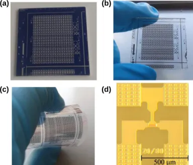
Figure 2.1- Thin film transistors on different substrates: (a) SiO2 dielectric based TFTs on Silicon substrate; (b) 7 layers multi-component Ta2O5/SiO2 dielectric based TFTs on Corning glass substrate and (c) on PEN substrate; d) micrograph of a a-ZTO TFT on Corning glass substrate.
Devices electrical characterization, transfer and output curves inspection, was performed using an Agilent 4155C semiconductor parameter analyzer connected to a Cascade Microtech M150 manual microprobe station, controlled by the software Metrics ICS. The Agilent measurements were done from different ranges depending on the sample used.
Stress measurements were performed using a semiconductor parameter analyzer (Keithley 4200-SCS) together with a probe station (Janis ST-500) under darkroom conditions at room temperature. Different TFTs channel lengths and widths were studied, as it will be reported in chapter 3.
(a) (b)
Sputtered Zn-Sn-O based thin-film transistors: Optimization and circuit simulation
9
3. Results and discussion
3.1 Thin Films Characterization
In general, the performance of AOS TFTs strongly depends on the channel layer preparation conditions, because the structural and chemical properties of the semiconducting oxide film are closely related to the field-effect phenomena, such as carrier mobility and drain current modulation. Many studies have examined the effects of the RF power [41]–[43], oxygen flow rate [44], [45], chamber pressure [46]–[48], and thermal annealing [49], [50] on the structural properties of metal oxide thin films and the resulting device performance of metal-oxide-TFTs.
In this work, the effects of the RF power, oxygen flow rate and of the incorporation of hydrogen during deposition of the ZTO layer were investigated.
3.1.1 Morphological and structural characterization 3.1.1.1 X-Ray Diffraction (XRD)
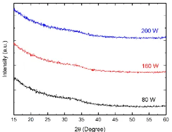
X-ray diffraction (XRD) measurements were used to give insight into the structural properties of the ZTO films. XRD plots of Zn-Sn-O thin films deposited at 10% oxygen flow, at different RF power (80 W, 160 W and 200 W) and annealed at 180 ºC are illustrated in Fig. 3.1 For all films only one broad peak with quite low intensity appears at 2θ = 34°, characteristic of amorphous zinc tin oxide films previously reported in literature [17], [51], [52]. It is observable that the amorphous structure is independent from the deposition power.
Figure 3.1 - XRD diffractograms of zinc tin oxide thin film deposited by sputtering at different powers on silicon substrate.
3.1.1.2 Energy-dispersive X-ray spectroscopy (EDS)
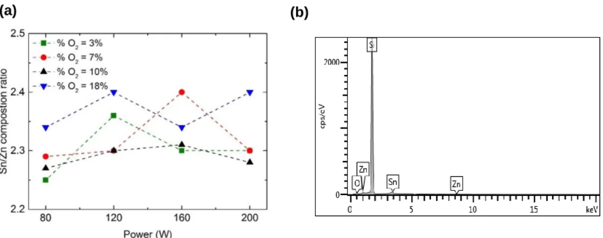
The film composition (Sn/Zn (at %) ratio) as a function of oxygen flow rate and RF power was determined by EDS, normalizing the peak intensity of Sn and Zn energies (Fig. 3.2b). Fig. 3.2a indicates that the thin film composition of Sn/Zn is maintained almost the same for all the deposition conditions and no contamination took place during or after the deposition. The Sn-Zn target used in this study has a 1:1 composition ratio, however a ~2:1 atomic ratio composition is calculated. Therefore, these data only provide relevant information about the apparent non-variation in the Sn:Zn atomic proportion.
Sputtered Zn-Sn-O based thin-film transistors: Optimization and circuit simulation
10 Figure 3.2- a) Sn/Zn atomic ratio dependence in thin films deposited with different power depositions in silicon substrates; b) example of an energy spectrum measured.
3.1.1.3 Scanning Electron Microscope (SEM) and Atomic Force Microscope (AFM) The films morphology and topography was analyzed by SEM and AFM respectively, for all the conditions deposited, presented in table 2.1. Fig. 3.3 shows the film morphology and topography for 80 W, 160 W and 200 W for the specific case of 10% of oxygen flow, during deposition. The SEM images were obtained at a magnification of 50 000. The surface is completely flat and, in agreement with XRD results, does not indicate any grain formation (Annex A).
Figure 3.3 – Morphological characterization of post-annealead ZTO thin films surface prepared at an O2% = 10%. Topography of ZTO thin films images of 2 x 2 µm2 surface area observed by AFM. Deposition power of (a),(d) 80W; (b), (e) 160W and (c),(f) 200W.
According to the AFM images, the films present a very smooth and uniform surface, for different powers. Moreover, the roughness is slightly decreasing with the power for the different oxygen percentages, wich can be justified by the film densification due to the increasing ions energy bombardment [57] (Annex B). (b) (b) (c) (c) (a) (a) (d) (a) (e) (a) (f) (a) (a) (b)
Sputtered Zn-Sn-O based thin-film transistors: Optimization and circuit simulation
11 3.1.2 Optical characterization
3.1.2.1 Growth rate of ZTO thin films
The power and oxygen flow impact on the growth rate of a-ZTO thin films was investigated through thickness measurements by spectroscopy ellipsometry. Fig. 3.4 shows a linear relationship with the deposition rate and with the RF power, as expected. A decrease in the growth rate with the decrease of O2% was also observed, showing a more effective influence for lower deposition powers.
Figure 3.4- ZTO growth rate dependence with power and oxygen variations for RT deposition at a 2.3 mTorr chamber pressure.
3.1.2.2 Transmittance and Ellipsometry
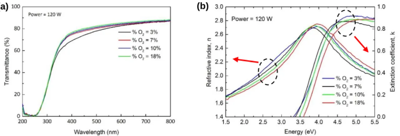
The transmittance of the sputtered zinc tin oxide thin films deposited on Corning glass, was measured by a Shimadzu UV‐3101 spectrophotometer in the wavelength range of 200-800 nm with a 3 nm step. Fig. 3.5a presents the optical transmittance spectra for a 40 nm thin film deposited at 120 W for different oxygen flow ratios. The average transmittance in the visible portion of the electromagnetic spectrum (400–700 nm) is above 70% for all conditions, reaching a maximum value of ~ 87% (Annex C).
The energy band gap (EG), refractive indices (n) and extinction coefficient (k) were determined from spectroscopic ellipsometry using a Tauc-Lorentz model, in an energy range of 1.5-5.5 eV, with a step of 0.05 eV. Fig. 3.5b presents the n and k behavior for different deposition conditions. As the oxygen increase, n is found to increase (Annex D).
Figure 3.5- Optical properties of thin films obtained by sputtering at a power of 120 W, with different %O2 deposited in a Corning glass: a) transmittance spectrum; b) Refractive index and extintion coefficient. The films were annealead at 180 oC for 1h.
(a)
(a)
(b)
Sputtered Zn-Sn-O based thin-film transistors: Optimization and circuit simulation
12 It is possible to notice that the transmittance decreases with decreasing the oxygen flow. This behavior is in good agreement with the findings obtained by Körner et al. in 2012. [14] Their study demonstrates that the additional deep levels present in the band gap are connected to point defects or small defect complexes, which reduce the transparency of a-ZTO films. In particular, they show that the broader defect band above the valence band in stoichiometric a-ZTO is due to undercoordinated single oxygen atoms whereas, the narrower one below the conduction band (average of ∼0.25 eV) is caused by strongly miscoordinated tin-oxygen atom complexes. Interestingly, while deepest states (even deeper than 0.25 eV) were localized at tin atoms with 4 or 5 nearest oxygen atoms, zinc atoms adjacent to oxygen-vacancy-like holes were found not to be a source of deep levels below the CB edge. They explain the different behavior of the zinc and tin atoms in the amorphous structures by their different valence. In fact, zinc requires ideally 4 oxygen next neighbors whereas tin prefers 6 oxygen neighbors, which is more difficult to fulfill. Therefore, since the deep levels below the CB arise mainly from undercoordinated tin atoms, the addition of oxygen could possibly reduce such defect levels.
Taking into account the abovementioned, increasing the oxygen flow during the ZTO film deposition would also lead to an energy gap increase, improving the transmittance. This assumption seems to be validated by the data presented in the Fig. 3.6a and Fig. 3.5a.
A decrease in the band gap for lower oxygen concentration was also reported by Barquinha et al. [53], which explained the phenomenon by the incomplete metallic Sn oxidation.
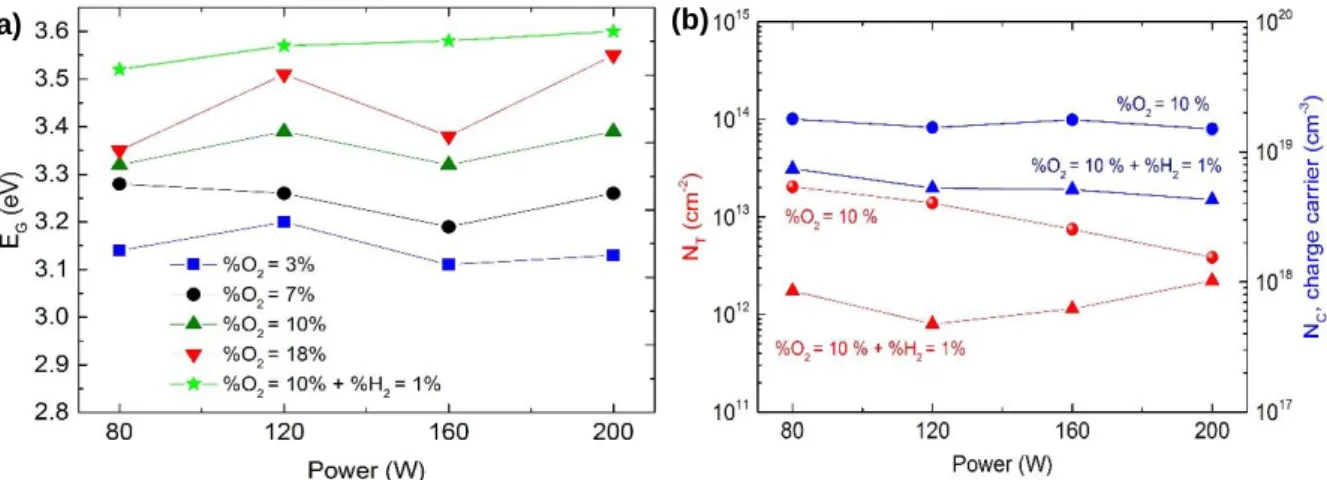
Figure 3.6- a)Dependence of the optical band gap (EG) as a function of RF power for different oxygen flow during ZTO thin films deposition. While the oxygen flow plays a relevant role in the optical band gap, no significant changes are seen with the power. b) Interfacial trap states and charge carrier concentration for thin films deposited with %O2 = 10% with and without hydrogen (1%).
The idea of Körner et al. could also support the general slight decrease of charge carrier concentration (NC) with the increase of oxygen that has been measured in this work. In fact, the carriers should originate from the formation of oxygen vacancies as shown in the following reaction [52],[54]:
𝑂0𝑥→
1
2𝑂2(𝑔) + 𝑉ö= 2𝑒
(3.1)
which indicates that oxygen on the oxygen sub-lattice (O0 x
) lost as oxygen gas (O2) creates a doubly charge oxygen vacancy (Vö) and two free electrons. Therefore, an oxygen pressure decrease, favors an increase in the free carrier concentration. This assumption is confirmed by the results (a)
a)
(b)
Sputtered Zn-Sn-O based thin-film transistors: Optimization and circuit simulation
13 achieved at lower powers, in which a NC decrease from 4.1x1019 cm-3 (%O2 = 3%) to 1.7x1019 cm-3 (%O2 = 18%) for 80 W and from 3.6x1019 cm-3 to 1.1x1019 cm-3 for 120 W.
The charge carrier concentration was calculated implementing the ZTO thin film as active layer in TFTs, using the equation 3.2 [55]:
𝑁𝐶=
𝐼𝐷𝑆𝐿
𝑞𝑉𝐷𝑆𝜇𝑠𝑎𝑡𝑊𝑑
(3.2)
In the reported work, a similar behavior, such as the increase of energy gap, transmittance and a decrease in free carriers was also obtained through the incorporation of H2. In fact, since deep levels above the valence band originate from undercoordinated oxygen atoms, hydrogen incorporation could suppress these levels by creating O-H bonds. [14] Fig. 3.6b shows the EG, NC and the interfacial trap states (NT)variation when H2 is added to a film grown with an oxygen percentage of 10%. It was found that by adding hydrogen, the charge carrier concentration decreases from 1.8x1019 cm-3 to 5.2 x1018 cm-3, the interfacial trap states decrease from 7.5 x1012 cm-2eV-1 to 1.1 x1012 cm-2eV-1 and the optical band gap increases ~0.2 eV.
The maximum density of surface states at the semiconductor/dielectric interface was calculated by employing characteristics of a ZTO channel based TFT, according to the following equation [56]:
𝑁𝑇𝑚𝑎𝑥 = (𝑆𝑆 𝑙𝑜𝑔(𝑒) 𝑘𝑇/𝑞 − 1) 𝐶𝑖 𝑞 (3.3)
where Ci is the dielectric capacitance, e is the electron charge, k is the Boltzmann constant and T is the room temperature value.
Besides, the power plays a significant role as many studies report [43][57][58]. In fact, as sputtering power increases, the kinetic energies of the sputtered atoms (Zn, Sn, and O) increase. Therefore, the energetic bombardment of these adatoms might change the interfacial properties of the channel film and affect the interfacial quality at the channel/gate insulator [57].
However, in this case of study, despite a slight decrease of RMS roughness (section 3.1.1.3), no other significant changes in morphological and optical properties were noticed for the RF powers range used.
Sputtered Zn-Sn-O based thin-film transistors: Optimization and circuit simulation
14 3.2 Electrical characterization of a-ZTO based TFTs
The main factors affecting the electrical properties of oxide TFTs include the active layer, gate insulator, and their interface [59]. In this section, the electrical characterization of a-ZTO thin film, implemented as a TFT channel, were studied under different deposition conditions (table 2.1). Moreover, a-ZTO optimized films were implemented in Corning Eagle glass and flexible substrate (PEN) using an oxide multilayer high-ƙ dielectric, providing enhanced devices performance. All the fabrication processes were pursued at temperatures below 180 oC.
3.2.1 Deposition parameters influence in devices performance 3.2.1.1 Oxygen and power impact in TFT performance
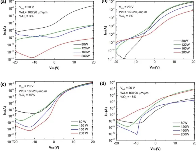
In order to study the a-ZTO based TFTs performance, a ~40 nm thick film was sputtered on silicon substrate, with a thermal 100 nm thick SiO2 dielectric. Later, source and drain electrodes were deposited with 60 nm thick Molybdenum (Mo). All the layers deposition took place by means of RF sputtering. At the end, devices were subjected to annealing at 180 oC in a hot plate for 1h in air. Fig. 3.7 shows the TFTs I-V curves obtained for all the different deposition conditions, for a VGS range of -20 V to 20 V, applying a constant VDS of 20 V. All the measured devices have a W/L ratio of 160 µm/ 20 µm.
Figure 3.7 - Tranfer curves of a-ZTO TFTs, fabricated under different oxygen flows and powers: a) %O2 = 3%; b) %O2 = 7%; c) %O2 = 10% and d) %O2 = 18%. All the devices were measured 3 days after fabrication.
(b) (b) (a) (a) (d) (d) (c) (c)
Sputtered Zn-Sn-O based thin-film transistors: Optimization and circuit simulation
15 Devices fabricated with 3% of oxygen flow show poor current modulation and an IDS decrease of almost 4 orders, from 10-5 A to 10-9 A, with power increase. On the other hand, it is noticed a channel current modulation by increasing the oxygen flow to 7%. However, when the power increases, the SS degrades and the VON shifts to more negative values. At 10% flow of oxygen, a good modulation is finally achieved with a maximum ION/IOFF of 4.2x10⁷ for 200 W. Interestingly, while the ION current remains constant, the IOFF decreases from 1x10⁻⁹ A to 1.8x10⁻¹² A with the power increase. Another effect noticed with the power increase is the SS degradation that can be explained by an interface traps states reduction, as shown in Fig. 3.6(b). A degradation in all the TFTs electrical characteristic parameters and no significant trends were observed for the highest oxygen flow.
In conclusion, the device showing the best electrical performance was the one fabricated with an %O2 of 10%. In fact, an higher ION/IOFF, lower SS and a non variation of ION with the power were observed. Despite the previous stated, a too negative VON (< -10 V) and a non satisfactory SS (> 2.8 V/dec) still represent an important limitation. Therefore, this condition of 10% of oxygen flow was further studied by the incorporation of hydrogen during the sputtering deposition.
3.2.1.2 Hydrogen impact in TFT performance
The fabrication procedure was the same used in the section 2.2, adding a H2 flow of 1% during the a-ZTO channel deposition. Fig. 3.8 shows the TFTs I-V curves obtained for the RF powers used in this study (80 W, 120 W, 160 W and 200 W). A VGS range of -5 V to 20 V was applied for a constant VDS of 20 V. All the measured devices have a W/L ratio of 160 µm/ 20 µm.
Figure 3.8 - Tranfer curves of a-ZTO TFTs fabricated with %O2 = 10% and %H2 = 1% for a power of a) 80 W; b) 120 W; c) 160 W and d) 200 W. Measurements were performed 3 days and 1 month after fabrication in order to check the TFT stability over time.
(b) (b) (a) (a) (d) (d) (c) (c)
Sputtered Zn-Sn-O based thin-film transistors: Optimization and circuit simulation
16 Table 3.1 - Summary of the electrical properties of a-ZTO devices with %O2 = 10% and %H2 = 1% for different RF powers.
Power (W) VON (V) VT (V) SS (V/dec) µsat (cm2/Vs) Hysteresis (V)
(3 days - 1 month) ION/IOFF
80 -3.0 6.95 0.61 0.86 5.02 - 6.67 7.1 x 10⁵
120 -1.5 4.89 0.31 1.40 2.98 - 6.78 3.3 x 10⁶
160 -1.5 6.73 0.42 1.90 1.97 - 2.28 5.4 x 10⁶
200 -3.8 6.17 0.76 0.85 3.80 - 2.50 4.0 x 10⁵
The incorporation of H2 in the channel layer structure lead to significant enhancement in the TFT performance, when comparing without its introduction. In fact, in the best case device, the SS decreases from 2.8 V/dec to 0.31 V/dec and the VON shifted towards more positive values (i.e. from -10 V to -1.5 V). Nevertheless, the ION current slightly decreases. Both the SS improvement and the IDS decrease are supported by the hypothesis of Korner et al. [60].
Table 3.1 presents the TFT key parameters, underlying a successful result for the device obtained with 160 W, with the higher ION/IOFF, VON closer to 0 V, the smallest SS and the best stability over time. Despite the achieved improvements, the low mobility is still not competitive for the requirements of the current technology and far from values achieved with other amorphous oxide semiconductors.
In this context, high-ƙ dielectrics become an attractive solution due to their high capacitances, low leakage current densities, smooth surfaces and high thermal stability [61], [62]. The combination of these characteristics allows to induce large charge densities in the semiconductor, thus increasing the mobility, and assure low voltage operations [63], [64].
Therefore, in the following section the results of optimized a-ZTO thin films implemented as active layer in TFTs with an oxide multilayer high-ƙ dielectric will be discussed.
3.2.2 Optimized TFTs with high-ƙ Ta2O5/SiO2 dielectric
As a final step in the a-ZTO TFTs optimization, staggered bottom-gate structure was adopted on both Corning Eagle glass and poly(ethylene naphthalate) (PEN) substrates. A 60 nm thick gate (Mo) was sputtered and patterned by liftoff followed by a deposition of a 100 nm seven layer multi - component oxide high-ƙ dielectric (Ta2O5/SiO2, ƙ = 11). Later, a ~40 nm thick amorphous ZTO channel layer was deposited. Source and drain electrodes were then deposited with a 60 nm thick Mo. All the layers deposition took place by means of RF sputtering at room temperature. At the end, devices on glass substrates were subjected to hot plate annealing at 180 °C for 1h in air, while devices on PEN substrate were annealed at 150ºC in hot plate for 1 hour in air.
Fig. 3.9 shows the TFTs I-V curves obtained for devices on both Corning glass and PEN substrates, with a channel length of 20 µm and different widths. VGS was swept between -4 V to 8 V, maintaining a constant VDS of 10 V.
Sputtered Zn-Sn-O based thin-film transistors: Optimization and circuit simulation
17 Figure 3.9 – Measured I-V characteristics for a-ZTO TFTs using an 100 nm thick TSiO dielectric layer. Effect of the channel width scaling with a fixed L = 20 µm on a) Coning glass and b) PEN substrate.
The desired enhanced mobility for low gate voltage operation, compared to the SiO2 based dielectric TFTs previously studied, was successfully achieved, confirming the high potential of high-k materials as a valid alternative for oxide TFTs technology. In addition, the 100 nm thichigh-k multilayer dielectric shows an excellent leakage current, proving to create a very good insulating interface with the semiconductor layer. Fig. 3.9 shows that as the channel width decreases, IDS is scaling down in both Corning glass and PEN substrates. a-ZTO based TFTs on PEN substrate show general lower performance if compared with the Corning glass substrate (Table 3.2). This can be due to the reduced annealing temperature, to which this flexible substrate is limitated in order to prevent possible mechanical stresses.
Table 3.2 - Summary of the electrical properties of a-ZTO optimized devices using a TSiO dielectric on Corning glass and PEN substrates.
The results presented in this work, are promising and further efforts in process optimization could promote the a-ZTO as the keystone material for an innovative transparent and flexible technology.
Substrate W / L (µm/µm) TA (oC) VON (V) VT(V) SS (V/dec) µsat (cm 2V-1s-1) ION/IOFF (A/A) Corning 160 / 20 180 -2.0 0.98 0.29 9.1 1.0x10⁷ PEN 160 / 20 150 -1.5 1.58 0.44 6.5 3.3x10⁶ (b) (b) (a) (a)
Sputtered Zn-Sn-O based thin-film transistors: Optimization and circuit simulation
18 3.2.2.1 Transmission Line Method (TLM)
Relevant information about the contact resistance on TFTs can be extracted through the Transmission Line Method (TLM), which have been already widely used in literature [65], [66]. The method consists in measuring several devices with different channel lengths (L) in the linear regime (low VDS), allowing the realization of the plot in Fig. 3.10, according to equation 3.4:
𝑅𝑇 =
𝑉𝐷𝑆
𝐼𝐷𝑆
= 𝑟𝑐ℎ𝐿 + 2𝑅𝑆𝐷
(3.4)
where RT is the total TFT on-resistance, rch is the channel resistance per channel length unit and
2RSD is the total (source and drain) series resistance. RSD includes the contributions of both the
contact itself as well as the semiconductor regions between the contact and the channel.
Figure 3.10 – a) Graphical examples of the main steps involved in the determination of contact resistance and intrinsic semiconductor parametrer by TLM; b) IDS and saturation mobility as a function of VGS for the a-ZTO TFT employed for TLM study.
The total TFT on-resistance shows a linear increment with L, as expected. As a matter of fact, rch
and 2RSD decrease with increasing VG. The large rch dependence on VGS is expected by the field
effect theory, since more carriers are being induced in the channel as VGS increases.
Regarding the RT dependence on the RSD, it was found out that its impact is always smaller comparatively to the channel resistance, proving that molybdenum creates a good interface with the semiconductor. This result demonstrates that intrinsic semiconductor and dielectric/semiconductor interface characteristics have more impact in the device properties, rather than contact undesirable effects.
rch values were used in order to obtain the intrinsic semiconductor mobility (i) and threshold
voltage (VTi) by the equation 3.5.
𝑟𝑐ℎ=
1 𝜇𝑖𝐶𝑖𝑊(𝑉𝐺− 𝑉𝑇𝑖)
(3.5)
i (12.4 cm2 V-1 s-1) and threshold voltage VTi (-1.8 V) were found to be slightly larger than FE (12.1 cm2V-1s-1) and VT (0.98 V). (b) (b) (a) (a) µ FE
![Figure 1.2 - Staggered bottom-gate TFT structure schematic used for this work, adapted from [4]](https://thumb-eu.123doks.com/thumbv2/123dok_br/15781211.1077000/27.892.114.799.159.458/figure-staggered-gate-tft-structure-schematic-used-adapted.webp)
![Figure 1.3 -Characteristic curves of an n-type oxide semiconductor-based TFT, with the output curves on the left and the transfer curves on the right [32].](https://thumb-eu.123doks.com/thumbv2/123dok_br/15781211.1077000/28.892.134.757.544.768/figure-characteristic-curves-semiconductor-output-curves-transfer-curves.webp)