Journal of Physics: Conference Series
Alternating-current and direct-current electrical
transport properties of diamond diodes with
diamond surfaces of the different morphology
To cite this article: A M Rodrigues 2009 J. Phys.: Conf. Ser. 193 012006View the article online for updates and enhancements.
Related content
A comparative study of numerical and analytical methods of simulating inhomogeneous Schottky diode characteristics
Subhash Chand and Saroj Bala
-Tunneling Current–Voltage Characteristics of Graphene Field-Effect Transistor Victor Ryzhii, Maxim Ryzhii and Taiichi Otsuji
-Modelling of Chirality-Dependent Current–Voltage Characteristics ofCarbon-Nanotube Field-Effect Transistors Zhao Xu, Wang Yan and Yu Zhi-Ping
Alternating-current and direct-current electrical transport
properties of diamond diodes with diamond surfaces of the
different morphology
A. M. Rodrigues
Departamento de Física, FCT, Universidade do Algarve, Campus de Gambelas, 8000-139 Faro, Portugal
E-mail:[email protected]
Abstract. The alternating current (ac) conductance (f=200 Hz) was measured as a function of
applied voltage at ambient temperature for two diodes with aluminium/diamond rectifying
contacts on chemical vapour-deposited diamond films of 5 m in thickness with different
morphology, nucleation and growth surfaces. Comparison of direct current (dc) conductance curves (deduced from experimental current–voltage curves) with ac conductance curves for the diodes revealed different transport mechanisms for two interfaces. The current–voltage characteristic of gold/diamond/gold structures shows that the two interfaces have different resistance values. The results demonstrate that the nucleation surface has a greater surface density of states than the growth surface, and this contributes to electrical transport through the potential barrier. Cole–Cole curves show a discrepancy between the Debye semicircle and experimental results and illustrate the fundamental differences between the two diodes. These results provide additional proof that the principal source of dispersion admittance is the surface
states. The current–voltage characteristic of diamond diodes with diamond films of 1 m in
thickness shows two distinct resistance states (high and low resistance). By applying an appropriate bias, resistance switching from one state to the other state can be achieved. The experimental results are discussed on the basis of filamentary conduction
1. Introduction
Carbon-based materials such as nanocrystalline diamond, polycrystalline diamond, amorphous carbon and carbon nanotubes are of immense scientific and technological interest in different fields such as electronics, electrochemistry, thermal applications, optics, and biology. The quality of the polycrystalline diamond films used in the present study is comparable to that of heteroepitaxial films reported in the literature [1]. Analysis of the diamond surfaces revealed that the growth surface was very rough, whereas the nucleation surface had a more uniform texture. Two types of structures were produced using diamond film of 5 m in thickness. One sample (designated S1) was prepared by depositing a rectifying aluminium (Al) contact on the diamond growth surface and the other (designated S2) by depositing a rectifying Al contact on the nucleation surface. As previously reported [2], the electrical properties of the devices are influenced by the surface morphology and microstructure. Investigation of the I–V characteristics revealed that the diode with a rectifying contact on the nucleation surface had better diode properties and lower conductivity. In the present study, complementary comparative studies of the alternating current (ac) and direct current (dc) conductance
EDISON 16 IOP Publishing
for the two different devices confirm our previous results [2] regarding charge transport. The impedance was measured and plotted in Cole–Cole representation for the growth surface and nucleation surface. The I–V characteristics of a similar device fabricated with a thinner diamond film (~1 m) are also described.
2. Experimental
The diamond filmused in this study was deposited on a n-type silicon substrate by MPCVD using a mixture of methane (1%) and hydrogen (99%). Details of the deposition conditions, substrate preparation, and quality of the diamond films can be found elsewhere [3, 4]. Diamond film of 1–5 m in thickness was obtained by removing the substrate with HF solution. The morphology of the two free surfaces was analysed by atomic force microscopy. This confirmed that the growth surface was relatively rough (~2% of the total film thickness) and formed by microcrystals with a common <111> orientation distributed homogeneously on the surface. Micro-Raman measurements showed no significant spectral differences for different regions of the surface. The nucleation surface was exposed after the substrate was removed and corresponds to the first layer of diamond deposition. This surface had an extremely flat morphology with average roughness ~4 nm, and a compact texture of very small, round grains. To produce the diodes, Au and Al contacts were deposited by thermal evaporation on opposite surfaces of the diamond film. Two types of diodes were prepared, with the rectifying Al contact on either the growth surface (S1 and S4) or the nucleation surface (S2). A symmetric structure, denoted S3, was prepared by depositing Au contacts on both diamond surfaces. Current–voltage measurements were performed using a Keithley 487 picoammeter/voltage source. Capacitance and conductance measurements were carried out in a vacuum chamber at a pressure of approximately 10–5 mbar using a Fluke PM6306 RLC meter with a resolution of 0.1 pF in the frequency range between 100 Hz and 1 MHz. Device fabrication and all electrical measurements were performed in the Centre for Electronics, Optoelectronics and Telecommunications, Algarve University.
3. Results and discussion
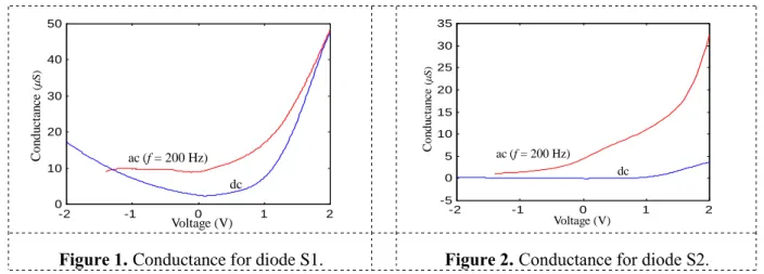
Analysis of the I–V curves for symmetric device S3 showed that the two diamond surfaces had different morphology and established electrical interfaces with the same metal (Au). The contact on the growth surface (rough surface) had lower resistance than the contact on the nucleation surface (flat surface) and this dissimilarity in resistance was responsible for the very small rectification. This observation prompted our first study of devices with rectifying Al contacts on diamond with two different surfaces [2]. To analyse the electrical transport mechanism in more detail and to complement the previous study, the dc and ac conductance of these devices was investigated in the present study. The I–V curves were derivative [2] to determine the dc conductance (dc) as a function of the applied voltage for devices S1 and S2. Figures 1 and 2 compare these results with the ac conductance (ac) as a function of the applied voltage, which was measured experimentally at a test frequency of 200 Hz at ambient temperature for each device. The curves for forward bias show that in general ac is greater than dc for both devices. For S1 the dc and ac curves tend to converge with increasing voltage, whereas for S2 the difference between the dc and ac curves increases with the voltage. These results indicate that the dominant electrical transport mechanism is different for each interface. In the S1 interface charge transport in the stationary regime predominates over charge transport in the alternate regime, in S2 the opposite is the case. This indicates that electronic states exist in the diamond gap that actively contribute to charge transport through the Schottky barrier. It is known that conduction in the ac regime is favoured by the presence of electronic states in the interface when the test frequency is sufficiently low so that the states can be filled and emptied during one cycle. In the stationary dc regime and for forward bias, all the electronic states are filled and consequently do not participate in electrical transport. The transport regime ac prevalence with Fermi energy dislocation in the direction of the conduction band indicates that the concentration of electronic states that participate in this
EDISON 16 IOP Publishing
Journal of Physics: Conference Series 193 (2009) 012006 doi:10.1088/1742-6596/193/1/012006
-2 -1 0 1 2 0 10 20 30 40 50 dc ac (f = 200 Hz) Voltage (V) C on du cta n ce ( S) -2 -1 0 1 2 -5 0 5 10 15 20 25 30 35 C on du cta n ce ( S) Voltage (V) ac (f = 200 Hz) dc
Figure 1. Conductance for diode S1. Figure 2. Conductance for diode S2.
process increases inside the forbidden band in the direction of the valence band of the diamond. The acceptor impurity concentrations obtained from a Mott-Schottky plot [2] for the growth and nucleation surfaces correspond at 61017 cm3 for S1 and 81016 cm3 for S2. The conclusion is that although the nucleation surface has a greater number of surface density states, the number of acceptor impurities is lower than for the growth surface.
Understanding of the physical origin of impurities is important when considering the growth process of the films. According to this model, the growth of crystals on the nucleation surface initially involves accumulation of diamond-like-carbon (DLC), followed by diamond growth in a planar region and finally by epitaxial growth of diamond normal to the surface of the substrate plane. This results in many small diamond grains with small inter-grain spaces on the nucleation surface. The growth surface has larger microcrystals and inter-grain spaces and a smaller number of microcrystals. Based on this growth model of the diamond films, it can be inferred that the nucleation surface is formed essentially of DLC whereas the growth surface is composed of diamond microcrystals and grain boundaries. Assuming that this model is adequate, it can be concluded that the carbon form found in the nucleation region is more easily compacted and thus accepts few impurities, but more surfaces states are generated.
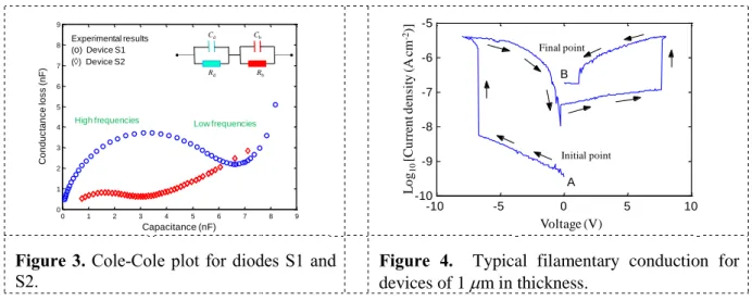
Admittance measurements provided more information about the nature of the two rectifying contacts and the role of morphology in the interface quality [2, 4]. Both devices were described by a simple equivalent circuit model (inset in Figure 3) for which the components Cd, Rd, Cb and Rb correspond to the capacitance and resistance of the depletion and bulk regions, respectively. A graphic representation of capacitance and conductance in the form of Cole–Cole plots for devices S1 and S2 is presented in Fig. 3. The fit parameters [2] are Cd=5 nF, Rd=0.4 M, Cb=0.2 nF and Rb=1 k for sample S1 and Cd=1 nF, Rd=0.5 M, Cb=0.3 nF and Rb=0.3 k for S2, in accordance with the electrical characteristics of the samples. For both devices the semicircle is flatter than a typical Debye curve, which is a perfect semicircle centred on the x-axis. Comparison of the curves for the two devices reveals greater compression for S2 than for S1, indicating that the former has greater admittance dispersion, which can be attributed to the surface states. Figure 3 also suggests another incomplete semicircle for low frequencies. This possibility exists because, as previously demonstrated [4], polycrystalline diamond can make two different contributions to admittance: due to grains at low frequencies and to grain boundaries at high frequencies. In this case a more complete circuit model that contains explicit grain and grain boundary characteristics is required.
Thinner films of approximately 1 m exhibited characteristics of filamentary conduction (device S4). Figure 4 shows a typical I–V curve for this device. Over a complete cycle originating at 0 V and traversing the voltage interval between –8 V and 8 V, a pronounced hysteresis is evident that is a consequence of the abrupt change from less conductor state to a more conductor state. These transitions occur at positive and negative voltage. The current density is relatively high and is two orders of magnitude greater than for the devices S1 and S2, and the noise is also higher. This high
EDISON 16 IOP Publishing
0 1 2 3 4 5 6 7 8 9 0 1 2 3 4 5 6 7 8 9 C o n d u c ta n c e lo s s (nF ) Capacitance (nF) Experimental results (o) Device S1 () Device S2 Low frequencies High frequencies Cd Cb Rd Rb -10 -5 0 5 10 -10 -9 -8 -7 -6 -5 -10 -5 0 5 10 -10 -9 -8 -7 -6 -5 A B L o g10 [Cu rren t d en si ty (A cm -2)] Voltage (V) Initial point Final point
Figure 3. Cole-Cole plot for diodes S1 and
S2.
Figure 4. Typical filamentary conduction for
devices of 1 m in thickness.
current density due to the change in states possibly corresponds to a mixture of electronic and chemical processes. This behavior is characteristic of filamentary conduction, which has also been observed for different amorphous inorganic semiconductors. Another feature of the samples was that no relaxation peak was observed in the ac admittance spectrum.
4. Conclusions
The I–V characteristic of symmetric devices revealed that the rough surface had lower resistance than the flat surface, causing extremely little rectification. Comparison of ac and dc conductance for the different aluminium/diamond interfaces revealed that the nucleation surface had a higher surface density that contributed to transport through the barrier. The dependence of this contribution on voltage suggests that this density increases of the interior of the forbidden band to valence band. This result is according with the literature [2] that considers that the nucleation surface has more defects. The surfaces states seem to have physical origin different of the accept impurities that contribute for bulk transport. The Cole-Cole plot shows a grade of the dispersion superior in interface of the nucleation surface indicating that the admittance dispersion apparently is due to surface states [2]. The fit parameters reflect the electrical conditions of the samples. The possibility of an incomplete semicircle at low frequencies suggests the possibility of two relaxation processes, one related to grains and the other to grain boundary regions of the diamond.
Current–voltage curves for diamond diodes with diamond films of 1 μm in thickness revealed that application of an adequate voltage leads to resistance switching between two distinct resistance states. These samples present characteristics of filamentary currents that have been observed in other semiconductors. Moreover, no relaxation peak was observed in the admittance curve for this device.
Acknowledgement
The author would like to thank Dr. H. Gomes of the Centre for Electronics, Optoelectronics and Telecommunications, Algarve University.
References
[1] Willander M, Friesel M, Wahab Q and Straumal B 2006 J. Mater. Sci. Mater. Electr. 17 1. [2] Rodrigues A M, Gomes H L, Rees J A, Pereira L and Pereira E 1999 Phys. Status Solidi (a)174
165
[3] Rodrigues A M 2008 J. Appl. Phys. 103 083708
[4] Rodrigues A M 2008 Diamond Relat. Mater. 17 1264 [5] Rodrigues A M 2007 Appl. Surf. Sci 253 5992
[6] Kao K C and Hwang W 1981 International series on the science of the solid state vol 14 (Oxford New-York: Pergamon Press)
EDISON 16 IOP Publishing
Journal of Physics: Conference Series 193 (2009) 012006 doi:10.1088/1742-6596/193/1/012006