Growth and Charaterization of OLEDs
with Europium Complex as Emission Layer
R.Reyes 1;2
, C.F.B. da Silva 3
, H.F. de Brito 3
, and M. Cremona 1
1
Departamento deFsia,PontifiaUniversidade CatoliadoRio deJaneiro,PUC-Rio,Brazil
2
FaultaddeIngenieraQumiayManufaturera,UniversidadNaionalde Ingeniera,Lima,Per u
3
Institutode Qumia,Universidadede S~aoPaulo,USP,Brazil
Reeivedon11Deember,2001
In this work the growth and the haraterization of red emitting triple-layer
eletrolumines-entorganideviesusingvauumdeposited(Eu(TTA)3(TPPO)2)europiumomplexas emitting
layer are desribed. The observed eletroluminesene (EL) is harateristi of the Eu 3+
emis-sion. Inthis devie the hole transportlayeris obtained usinga thinlm of
1-(3-methylphenyl)-1,2,3,4 tetrahydroquinoline-6-arboxyaldehyde-1,1'-diphenylhydrazone (MTCD), while the
tris(8-hydroxyquinolinealuminum)(Alq
3
)isusedaseletrontransportlayer(ETL).
I Introdution
Inthelastyears,eletroluminesene(EL)fromorgani
thinlmshasbeomeamatterofgreatinterestbeause
ofits potentialtoenablelow-ost,fullolor,atpanel
displaysandotheremissivedevies[1℄. Byseletingthe
appropriateemittinglayer,thelightemissionouldbe
hangedthroughalmostthewholevisibleregion. Sine
TangandVanSlyke[2℄reportedtherstarhitetureof
thedouble-layeredorganiELdevie,manyresearhers
havedevelopedhighperformanegreenorganiEL
us-ingtris(8-hydroxyquinolinate)aluminum(Alq
3
)[3,4,5℄.
BrightblueorganiELdeviehavebeenreportedusing
5,5'-bis(dimesitylboryl)-2,2'-bithiophene (BMB-2T) as
dopant in N-arylbenzimidazole (TPBI)[6℄. Some
or-angeandredorganiELdeviesusingsomeomplexes
and/or organi dyes have been disussed [7,8℄.
Eu-ropiumomplexhavebeenappliedbyseveralresearhes
as emittingmaterials in red-emittingEL devies with
sharpspetra[10-14℄.
There are two main advantages in fabriating EL
devies using rare earth omplexes: (i) theoretially
the upper limit of inner quantum eÆieny is near
100%, whih is four times higher that of similar
de-vies using other materials; and (ii) the sharp
emis-sion bands of rare earth ions is verysuitable for
full-olor display. In partiular, Eu 3+
ions are known to
be weakly uoresent speies due to their low
quan-tum yields andpoor molarabsorption. Thetehnique
of ligand sensitized uoresenehas been found to be
an eÆient method for enhaning its uoresene. In
this method, an organi ligand with a higher molar
absorption is omplexed with the Eu 3+
. On
exita-of its exitation energy to the higher energy levels of
Eu 3+
, whih then emits. Suh an indiret way of
exitation results in the uoresene enhanement of
Eu 3+
ompared to diret one. A number of organi
ligands suh as -diketones, aromati arboxyli aid
orpolymers have been used as sensitizing ligands for
this purpose [11,15,16,17℄. Generally, in EL devies
using europium omplexes the
N,N'-diphenyl-N,N'-bis(3-methylphenyl)-1,1'-biphenyl-4,4'-diamine (TPD)
is used as Hole Transport Layer (HTL), [10, 11, 13,
14℄. PVKandNPBwasalsousedinotherdevies[12℄.
This work is based on the use of the
1-(3-methylphenyl)-1,2,3,4,
tetrahydroquinoline-6-arboxyaldehyde-1,1'-diphenylhydrazone (MTCD) as
hole-transportlayerinanorganiLEDwherethe
emit-ting layer is onstituted by the Eu(TTA)
3
(TPPO)
3
omplex. Whenthisdevieispolarizedwithan
appro-priatevoltagebiasitispossibletoobserveabrightred
light. The preparation, the haraterization and the
ELpropertiesof thisdevies willbealsodisussed.
II Experimental
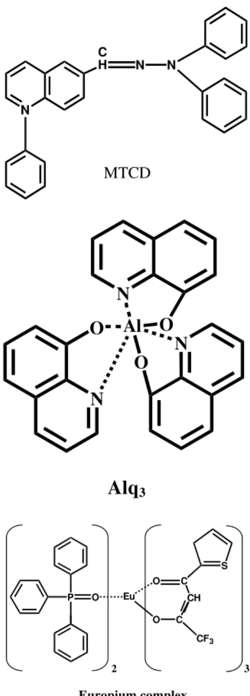
Figure1showsthehemialstruturesoftheused
ma-terials while in Fig. 2is reported the arhiteture of
theELdiode.
In our devie, the
1-(3-methylphenyl)-1,2,3,4
tetrahydroquinoline-6-arboxyaldehyde-1,1'-diphenylhydrazone (MTCD) is used as Hole T
rans-port Layer (HTL), while the tris(8-hydroxyquinoline
aluminum) (Alq
3
thenoyltriuoroaetonate)bis(triphenylphosphine
ox-ide)europiumomplex(Eu(TTA)
3
(TPPO)
2
)isused.
N
C
H
N
N
MTCD
N
O
Al
O
N
O
N
Alq
3
P
O
Eu
O
O
C
CH
S
C
CF
3
2 3
Europium complex
Figure1. Moleularstrutureoftheusedmaterials.
The MTCD was kindly donated by Prof.
Sung-HoonKimoftheDepartmentofDyeingandFinishing,
of the Kyunpook National University (South Korea)
and wasusedasobtained. TheAlq
3
wasused as
pur-hasedfromAldrih. Finally,the[Eu(TTA)
3
(TPPO)
2 ℄
europium omplex was prepared asfollows: hydrated
preursor [Eu(TTA)
3 (H
2 O)
2
℄ was dissolved in ethanol
andTPPO,alsodissolvedinethanol,wasaddedtothe
solutionin the molarratio 1:2(salt : ligand).
Sues-sively,thesolutionwasallowedtomixuntilthe
forma-wastwiepuriedwithaetoneandthendesiatedin
vauum.
The substrate for EL devie fabriation is an
indium-tin-oxide(ITO)oatedglasswithasheet
resis-taneof8.1=2. Thesubstrateswereinitiallyleaned
byultrasoniationrstusingadetergentsolution,
fol-lowed by toluene degreasing, and then leaned newly
by ultrasoniation with pure isopropyl alohol.
Af-ter dryingusing aninfraredlamp,the substrateswere
loadedintothevauum hamber.
Figure2. EudopedOLEDarhiteture. EListheEu
dopedlayer.
Theorganiompoundsweresuessivelythermally
evaporatedonto ITOatroomtemperaturefrom
tung-sten ruibles with rates in the range of 0.1-0.3nm/s
belowapressureof5x10 5
Torr.TonalizetheEL
de-vieanaluminumathodewasevaporatedfroma
tung-stenwirebasketathigherrates(about1.0nm/s)inthe
samevauumhamber. Thelayerthiknesswasinsitu
ontrolledthroughaquartzrystalmonitor. The
emis-sionareawas50mm 2
typially.
Photoluminesene(PL)andELspetrawere
mea-sured with a Photon Tehnology (PTI) Fluoresene
spetrophotometer. The brightness was measured by
using a alibrated radiometer/photometer by United
Detetor Tehnology, model 350. All measurements
were arried out at room temperature under ambient
atmosphere.
III Results and disussion
Redanduniformlightemissionwasobservedfrom the
produed organi EL devie, when a positive voltage
wasapplied to the ITO eletrode. The organidiode
shown in Fig. 2 an operate both in ontinuos (d)
and/or pulsed mode. Its eletrial behavior is
simi-lar to that of a retier diode, the forward bias
or-responding to a positive voltage applied to the ITO
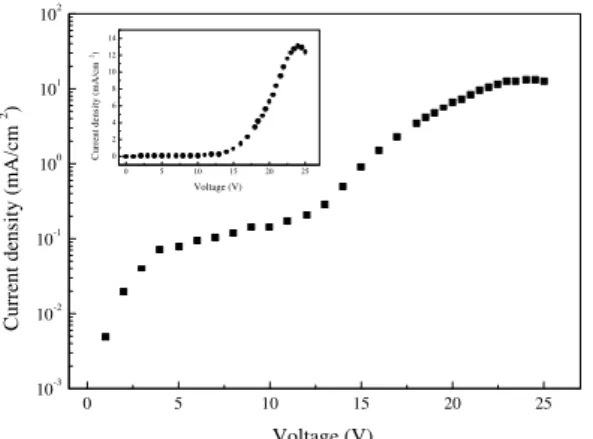
eletrode. Figure 3shows theontinuosd urrent vs
voltage(I V)urve. Duringtheexperimentswenoted
that someof the produed ELdevies showed a
thedevie,theshortiruitopens,andthedeviestart
to emit light. This behavior suggeststhe presene of
mirosopiondution pathsthroughtheorgani
lay-erswhihareburnedoutonappliation ofhigher
ur-rents. The existene of these paths at the rst stage
of OLEDoperationanbedue to theexisteneofnot
gooduniformityatoneorbothoftheorgani/eletrode
interfaes,whihmayleadtononuniformeletrields
arossthedevie. Thisanresultsin theformationof
high urrent\hotspots"orshort iruits[18℄.
0
5
10
15
20
25
10
-3
10
-2
10
-1
10
0
10
1
10
2
0
5
10
15
20
25
0
2
4
6
8
10
12
14
Current density (mA/cm
2
)
Voltage (V)
Current density (mA/cm
2
)
Voltage (V)
Figure3. I-Vurveofthedevie. Theinsetshowsthesame
behaviorinalinearsale.
Figure 4 shows the EL spetrum harateristi of
the Eu 3+
emission where the peaks at 540, 579, 590,
615,650nmorrespondrespetivelytothe 5 D 1 ! 7 F 1 , 5 D 0 ! 7 F 0 , 5 D 0 ! 7 F 1 , 5 D 0 ! 7 D 2 , 5 D 0 ! 7 F 3
transi-tionsoftheeuropiumion. Inthespetrumitispossible
to observe the main emission peak at 615 nm
orre-spondingto the 5 D 0 ! 7 F 2
transition of Eu 3+
ion. So
thedevieemitshighly monohromatiredlight.
400
450
500
550
600
650
700
0
20
40
60
80
a
b
c
a: 15.0 V
b: 17.5 V
c: 20.0 V
EL Intensity (arb. units)
Wavelength (nm)
Figure4. ELspetrafor theEudopedOLEDfor dierent
valuesofbiasvoltage(a=15V,b=17,5 V,=20V).
Generally,in lanthanide metalomplexes, the
en-tral metal ion M 3+
is exited through the exitation
of theligand [12℄. Thus, theELproess of thedevie
an be understood as following. Under ELoperation,
eletronsaretransportedintothe[Eu(TTA)
3
(TPPO)
2 ℄
omplexlayerfromtheAlq
3
lm,whileholesare
trans-Theexitationoftheligandisthenrealizedby
ombina-tionof theeletronsandholes. Afterward,theexited
energyin the ligand is transferred to the entral ions
throughtheligand'stripletenergylevel[19℄andnally
theemissionoftheEu 3+
ionsisobserved.
Figure5shownaomparisonbetweentheEL
spe-trumoftheITO/MTCD/[Eu(TTA)
3 (TPPO) 2 ℄/Alq 3 /Al
OLED devie and the PL spetrum taken from a
[Eu(TTA)
3
(TPPO)
2
℄thermallydepositedthin lm
ex-itedwith=350nm. Thetwospetraweremeasured
atroomtemperature. Asit ispossibleto see,thetwo
spetra are quite similar, exept that sometransition
intheELspetrumdoesn'tappearso strongasin the
PLone, as for example in the ase of the 5 D 0 ! 7 F 1
transition. Moreover, the typial Alq
3
wide emission
band,peakedat520nm,isabsentinthePLspetrum.
This result is dierent with respet to that found by
H. Caoet al.[13℄ and it is still under investigation. A
possibleexplanationanbedue totheenergytransfer
from thetripletto the Eu 3+
ionthat is quiteeÆient
andanquenh theAlq
3
luminesene.
500
550
600
650
700
0.0
0.2
0.4
0.6
0.8
1.0
0.0
0.2
0.4
0.6
0.8
1.0
PL (l
exc
=350 nm)
EL (22 V bias)
PL Intensity
EL Intensity
Wavelength (nm)
Figure 5. PL and EL spetra for a [Eu(TTA)
3
(TPPO)
2 ℄
thermally deposited thin lm and the Eu doped OLED
respetively. The PL spetrum was taken exiting with
= 350 nm. In the ase of the EL spetrum, the bias
voltageusedwas22V.
In this gure it is also possibleto observea small
shiftoftheELband with respet tothePLone. The
displaement is of the order of 2 nm and it is real,
notdependingfrominstrumentalfators. However,the
FWHMofbothofthespetraisalmostthesameandits
valueisaboutof0.03eV.Alsothiseet,whihanbe
duetothedierentnatureofthemehanismsinvolved
forthePLandtheELemissions,isunderinvestigation.
Figure 6 shows the luminane vs voltage urve of
ourOLED devie. The light emission start to be
de-tetedaround12V, withaluminane of 0.01d/m 2
.
Theluminanegrowslinearlywiththeappliedvoltage.
Themaximumluminaneobtainedwiththisdeviewas
about2.2d/m 2
applying23Vbiasvoltage. Thisvalue
isin good agreementwiththat obtainedbyH. Caoet
voltageinadierentdevie whihusestheTPD
om-poundasHTLlayer. Inreasingthevoltagemorethan
23V resultsin adereasingofthe ELemissiondue to
knowndegradationeets[20,21℄.
0
5
10
15
20
25
10
-3
10
-2
10
-1
10
0
10
1
0
5
10
15
20
25
0.0
0.5
1.0
1.5
2.0
2.5
Luminance (cd/m
2
)
Voltage (V)
Luminance (cd/m
2
)
Voltage (V)
Figure6. TheluminanevsbiasvoltageurvefortheEu
dopedOLED.
0
2
4
6
8
10
12
14
0.0
0.5
1.0
1.5
2.0
2.5
Luminance (cd/m
2
)
Current Density (mA/cm
2
)
Figure7. TheluminanevsurrentdensityurvefortheEu
dopedOLED. Itis possible tosee thegood linearity from
0.1to13mA/m 2
.
TheOLEDlightoutput asafuntion of theinput
urrent wasalso measured and it is shown in Fig. 7.
Theemissionfromthediodeislinearintherangefrom
0.1to13mA/m 2
.
The13mA/m 2
valueorrespondingtoabias
volt-ageof23V.Upthisvoltage,theurrentdereasesand
itispossibletoobservesmallsparksinthedevie,while
theluminanedereasetoo. Inthisasethedevie
be-gintoworkasaapaitor,thehargetransport isless
eÆient in the organilayers,and theintense eletri
eld (10 8
V/m) ausesadieletri breakdown
start-ingtodamagetheorganimoleuleswhihomposethe
Bydividing theluminane forthe urrent density,
we andene another important item that is the EL
emission eÆieny havingthe dimensionsof d/A.As
anbeseeninFig.8,inourOLEDtheeÆienygrows
withtheappliedvoltage. Inpartiular,intheregion
be-tween13and17V, theeÆieny growsmonotonously.
Startingfrom thispoint,afurtherinreaseofthe
volt-agedoesnotorrespondtoaninreaseintheeÆieny.
Thismeaningthatthereisalossofurrent,i.e. notall
theurrentis onvertedin light. Inthepresentdevie
theeÆieny reahesitsmaximumvalue(de1.7x10 2
d/A)for23Vofbiasvoltage. Thisrelativelylowvalue
oftheeÆienywhenomparedwithothersOLEDsan
beprobablyasribedto thetypialEuropiumomplex
behaviorwhenused aslightemitterinaorganiLED.
Indeed,eventhoughthispartiularomplexhasahigh
quantum eÆieny of uoresene when exited with
photons, itsEL eÆieny fall at low valueswhen itis
used asemitting layerin OLEDs,due probablyto the
lossesintheligand-Eu 3+
energytransferproess.
0
5
10
15
20
25
30
0.000
0.004
0.008
0.012
0.016
0.020
EL Efficiency (cd/A)
Voltage (V)
Figure 8. EL eÆieny vs bias voltage urve for the Eu
dopedOLED.After20Vbeginthedieletribreakdown
ef-fet, lowering the eÆieny and the luminaneof the
de-vie.
Generally, the morphologial properties of the
or-gani layersare ritial in the fabriation of
optoele-tronithin-lmdevies. Inpartiular,fortheOLEDsit
isneessarythatallthelayersthatonstitutethedevie
musthavelowroughnessvaluesandhighhomogeneity.
Moreover,thelowvalueoftheTg(glasstransition
tem-perature)for theHTL layerit is an importantfator
in the degradation proess. Indeed, by observing the
MTCDthin lmsthermallyevaporatedontoglass
sub-strates some hours after the deposition proess, it is
possibleto detetsomekind ofrystallization in form
of \leaf" (see Fig. 9). This rystallization, already
observed in other systems[22℄,dereases theemission
Figure 9. Crystallization eet in a thin lm of MTCD
somehoursafterthedepositionobservedattheoptial
mi-rosope(x500).
IV Conlusion
Triple-layer eletroluminesent organi devies
us-ing 1-(3-methylphenyl)-1,2,3,4
tetrahydroquinoline-6-arboxyaldehyde-1,1'-diphenylhydrazone (MTCD) as
theholetransportlayer,Eu(TTA)
3
(TPPO)
2
europium
omplexastheemissionlayerandtheAlq
3
asthe
ele-trons transport layer were grown and haraterized.
Photoluminesene(PL)andeletroluminesene(EL)
spetra were reorded at room temperature and
om-pared. Inboththespetraitispossibleto identifythe
typial Eu 3+
sharp emission line. Work is urrently
in progress to produe others organolanthanide-based
eletroluminesentdevies.
Anowledgements
The authors thank Prof. Sung-Hoon Kim of the
DepartmentofDyeingandFinishing,oftheKyunpook
NationalUniversity(SouthKorea)fortheMTCD
ma-terial. This work was supported by CNPq, FAPERJ
andFAPESP.
Referenes
[1℄ J.R.Sheats,H.Antoniadis,M.Hueshen,W.Leonard,
J.Miller,R.Moon,D.Roitman,andA.Stoking,
Si-ene273,884(1996).
[2℄ C.W.TangandS.A.VanSlyke,Appl.Phys.Lett.51,
913(1987).
[3℄ C.W.Tang, S.A. VanSlyke,and C.H.Chen, J.Appl.
Phys.65,3610(1989).
[4℄ C.Adahi,K.Nagai,andN.Tamoto,Appl.Phys.Lett.
66,2679(1995).
[5℄ G.Giro,M.Cohi,P.DiMaro,E.DiNiolo,V.
Fat-tori,J.Kalinowski,andM.Ghedini,Synt.Metals102,
1008(1999).
[6℄ B. Chen, X.H. Zhang, X.Q. Lin, H.L Kwong, N.B.
Wong,C.S.Lee,W.A. Gambling,andS.T.Lee,Synt.
Metals118,193(2001).
[7℄ C.Adahi,S.Tokito,T.Tsutsui,andS.Saito,Jpn.J.
Appl.Phys.27,L269(1998).
[8℄ J.KidoandJ.Endo,Chem.Lett.7,633(1997).
[9℄ R.J. Curry and W.P. Gillin, Synt. Metals 111, 35
(2000).
[10℄ K.Okada,Y.Wang,andT.Nakaya,Synt.Metals97,
113(1998).
[11℄ Y.Miyamoto, M. Uekawa,H.Ikeda, and K.Kaifu, J.
ofLumines.81,159(1999).
[12℄ C.J. Liang, Z.R. Hong, X.Y. Liu, D.X. Zhao, D.Z.
Zhao,W.L.Li,J.B.Peng,J.Q.Yu,C.S.Lee,andS.T.
Lee,ThinSol.Films359,14(2000).
[13℄ H.Cao,X.Gao,C.Huang,Appl.SurfaeS.161,443
(2000).
[14℄ N.Takada,J.Peng,andN.Minami,Synt.Metals121,
1745(2001).
[15℄ H.F.Brito,O.L.Malta,andJ.F.S.Menezes, J.Alloys
Comp.336,303(2000).
[16℄ O.L. Malta, H.F. Brito, J.F.S. Menezes, F.R.
Gonalves,S.A.SilvaJr,F.S.Farias,andA.M.de
An-drade,J.Lumin.75,255(1997).
[17℄ C.Liang,W.Li,Z. Hong,X.Liu, J.Peng, L.Liu,Z.
Lu,M. Xie,Z.Liu, J.Yu,andD. Zhao,Synt.Metals
91,151(1997).
[18℄ P.E.Burrows,V.Bulovi,S.R.Forrest,L.S.Sapohak,
D.M.MCarty,andM.E.Thompson,Appl.Phys.Lett.
65,2922(1994).
[19℄ G.A. Crosby, R.E. Whan, and R.M. Alire, J. Chem.
Phys.34,743(1961).
[20℄ H.AzizandG.Xu,Synt.Metals80,7(1996).
[21℄ Lee-M.Do, M. Oyamada,A. Koike, Eun-M.Han, N.
Yamamoto,andM.Fujihira,ThinSolidFilms273,209
(1996).
[22℄ Eun-MiHan,Lee-MiDo, N.Yamamoto,andM. F