Brazilian Microwave and Optoelectronics Society-SBMO received 17 Apr 2018; for review 23 Apr 2018; accepted 7 Nov 2018 Brazilian Society of Electromagnetism-SBMag © 2018 SBMO/SBMag ISSN 2179-1074
Abstract— In this article, equivalent circuit modeling with study and analysis of band notch characteristics for a triple band notched UWB antenna has been discussed to develop a better understanding of the antenna functioning and its behavior. A small square ultra wideband antenna having overall size of 24 x 31 mm2 with tri- band rejections is designed and simulated using HFSS software. Very narrow band notching is accomplished by placing C slots and inverted C slot of different dimensions on the radiating patch which makes maximum space utilization without performance deterioration. The antenna operates from 3.1 to 14 GHz (VSWR < 2) with the presence of 3 narrow band notches (VSWR >2) of 3.3- 3.7 GHz (WiMAX), 5.1 - 5.4 GHz (Lower WLAN and HIPERLAN/2) and 5.7 – 6 GHz (Upper WLAN) as shown by the simulated and measured results (VSWR<2) of the UWB antenna, with and without the presence of triple notches, thus utilizing the maximum UWB bandwidth. The radiation pattern plots for simulated and measured results are also presented to validate the working of the antenna. This antenna can be a respectable candidate for future European and USA high capacity UWB applications. The group delay and peak gain plots are also found to be stable in the range of operation of the antenna. The study and analysis of the band notching is discoursed in terms of current distribution and impedance plots to provide a greater and better perception into the working of the antenna and hence an equivalent circuit for the tri-band notched UWB antenna has been proposed.
Index Terms—UWB planar antennas, Tri-band notching, Slots, optimization, Equivalent circuit, Wireless communication.
I. INTRODUCTION
The field of wireless communication has witnessed swift and tremendous technological development in the recent years, with enormous impetus in research in the planar UWB antenna technology field because of their attractive properties of low power consumption, the provision for providing high data rate multimedia services with low cost and compact sized circuitry.
The availability of 7.5 GHz (3.1 GHz - 10.6 GHz) of bandwidth for UWB applications by the Federal Communications Commission (FCC) [1] has further been the cause of a spurt of significant researches in the UWB technology area.
Parametric study and Analysis of Band Stop
Characteristics for a Compact UWB Antenna
with Tri-band notches
Qurratul Ain, Neela ChattorajBrazilian Microwave and Optoelectronics Society-SBMO received 17 Apr 2018; for review 23 Apr 2018; accepted 7 Nov 2018 Brazilian Society of Electromagnetism-SBMag © 2018 SBMO/SBMag ISSN 2179-1074
Nevertheless, the technical hurdles due to the increase in spectrum congestion, interference due to existing systems etc. have to be met in the designing of UWB antennas. Frequency rejection technique is an attractive way to reduce interference between the UWB systems and existing wireless systems without increasing the size or footprint of the antenna [2]. Many kinds of planar UWB antenna designs with notching have been designed and presented [3]-[13]. One of the foremost frequency rejection design technique that meets the need of the current scenario is the incorporation of slots in the antenna patch or in the ground plane so that it does not require any extra space for its implementation [3],[4],[6],[7]. Slots can be varied in geometry, shape, size and constitution, thus ensuing in the conception of different frequency notch bands. Consequently, several conception strategies for band notching using slots have been embraced making use of various anatomies for slots, such as U-shape [7], C-shape [6], annular slots [11], I-shape [12], H-shape [12] and so on. The intended antenna design incorporates the important essentials for developing an optimum UWB antenna for UWB technology.
This paper is structured as follows. Section II outlines the design proposal of a triple band-notched compact UWB antenna with notches at 3.3-3.7 GHz (WiMAX), 5.15-5.35 GHz and 5.725-5.825Ghz (WLAN) with the design equations and dimensions. In section III experimental results for the designed antenna are presented and discussed to validate the performance of the antenna. The simulated current distribution as well as the impedance plots are discussed to understand the physical concept of frequency band notching and finally an equivalent circuit representation for the UWB antenna is proposed in section IV.
II. ANTENNA CONFIGURATION AND DESIGN OPTIMIZATION
A. Basic UWB antenna details
The snapshots of the final antenna geometry of main reference antenna are shown in Fig. 1(a) & (b). The antenna is fabricated on the easily available and cost effective FR4 substrate having ϵr = 4.4
and substrate height of 1.6 mm and loss tangent 0.02.
(a) (b)
Brazilian Microwave and Optoelectronics Society-SBMO received 17 Apr 2018; for review 23 Apr 2018; accepted 7 Nov 2018 Brazilian Society of Electromagnetism-SBMag © 2018 SBMO/SBMag ISSN 2179-1074
The following formulae constitute the starting point for basic calculations for the antenna dimensions which are then used to design and simulate the reference antenna [14], [15]:
The length of the patch of antenna is given as follows: L L
reff r
f
2
2 1
0 0
(1)21 12 1 2 1 2 1 W h r r reff
(2)
) 8 . 0 )( 258 . 0 ( ) 264 . 0 )( 3 . 0 ( 412 . 0 h w h w h L reff reff
(3)where L is the length, fr is resonant frequency, ϵr is relative permittivity, ϵreff is effective permittivity
whose formula is mentioned in (2) and ΔL is incremental length as shown by (3).
Width of patch is given by: 1 2 2 1 0 0
r rf
W (4)
Feed line width is calculated as follows:
2 ) 2 exp( ) exp( 8 A A h wfeed (5)
where wfeed is feed line width, h is the thickness of the substrate and A is given by the formula
mentioned below.
{0.23 0.11}
1 1 } 2 1 {
60 0.5 r r
r r
c Z
A
(6)
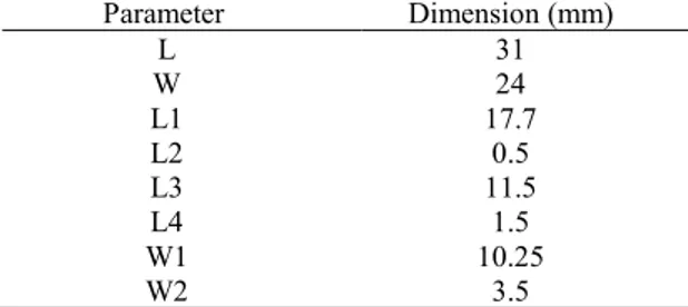
Table I provides the optimized dimensions for the main reference UWB antenna.
TABLEI. OPTIMIZED DIMENSIONS OF UWB REFERENCE ANTENNA STRUCTURE
Parameter Dimension (mm)
L 31
W 24
L1 17.7
L2 0.5
L3 11.5
L4 1.5
W1 10.25
W2 3.5
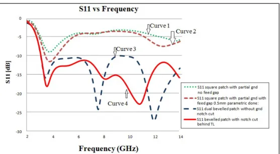
In Fig. 2 the steps of antenna design evolution are shown which clearly portray the progression of the design steps. Fig. 3 shows simulated S11 curves for the different stages of the basic reference
Brazilian Microwave and Optoelectronics Society-SBMO received 17 Apr 2018; for review 23 Apr 2018; accepted 7 Nov 2018 Brazilian Society of Electromagnetism-SBMag © 2018 SBMO/SBMag ISSN 2179-1074
mentioned in step 1 of Fig. 2, with partial ground length 12 mm (without any feed gap). It is observed that desired result is not obtained. The curve 2 in Fig. 3 shows S11 values of the same square patch
with partial ground length (feed gap 0.5 mm). It is observed that the antenna bandwidth of 3.5 GHz - 4.3GHz is obtained. The beveling technique is used at both corners of the radiator for bandwidth enhancement in the reference antenna as shown in step 2 of Fig. 2. The effect of beveling is clearly seen by curve 3 in Fig. 3. It is observed that a very wide bandwidth (S11 < -10dB) of 3.1GHz - 14GHz
is obtained for the dual beveled radiator with partial ground length of 11.5 mm. Further refinement in the reference antenna design was achieved when a notch cut in the partial ground plane is introduced exactly behind the transmission line. This leads to better impedance matching over the entire obtained wide bandwidth of 3.1GHz -14 GHz, as shown by curve 4 in Fig. 3.
B. Single band notched UWB antenna details
Fig. 4 displays the proposed designs of the antennas A, B and C in step 3, which incorporate band stop structures at the three applications that can cause interference with the UWB systems (vice versa) which are WiMAX, Lower WLAN, and Upper WLAN respectively. Thus, the three frequency bands
Fig. 2. Evolution stages in reference antenna design
Brazilian Microwave and Optoelectronics Society-SBMO received 17 Apr 2018; for review 23 Apr 2018; accepted 7 Nov 2018 Brazilian Society of Electromagnetism-SBMag © 2018 SBMO/SBMag ISSN 2179-1074
can be blocked by including band stop resonating structures, in our case slots, on the radiating patch of the reference antenna as shown in step 4 of Fig. 4.
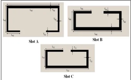
Slot lengths for simulation are derived from:
eff SLOT CENTERL
f
2 c (7)where fcenter is the resonant frequency of notching, Lslot is the total length of the slot, ϵeffis the effective
dielectric constant and c is the speed of light. The slot length is considered as equal to the half wavelength at the resonant frequency of notching, i.e., fcenter. The three resonant frequencies (fcenter) for
the three slot designs are 3.5 GHz, 5.2 GHz and 5.7 GHz, respectively. Based on the formula mentioned above we observe that the fcenter is inversely proportional to the slot length. Thus, when
designing slot for the lower resonant frequency f3.5, the calculated slot length is 26.13 mm. Similarly
for f5.2 and f5.7 the calculated slot lengths are 17.59 mm and 16.05 mm, respectively.
The geometry of the slot considered in the simulation has to be such that the entire length of slot can be etched on the radiator without degrading the antenna performance. Fig. 5 displays the geometry of the slots A, B and C, incorporated on antennas A, B and C, respectively, thereby creating 3 single band notched antennas.
Brazilian Microwave and Optoelectronics Society-SBMO received 17 Apr 2018; for review 23 Apr 2018; accepted 7 Nov 2018 Brazilian Society of Electromagnetism-SBMag © 2018 SBMO/SBMag ISSN 2179-1074
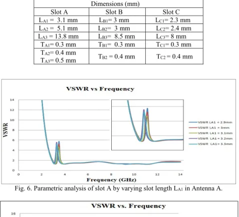
Parametric analysis based on the length of the slots is done to show how the frequency notch bands are controlled by them. The length LA1 of slot A is varied from 2.9 mm to 3.2 mm as shown by
simulated VSWR curves for different values of LA1 in Fig. 6. We observe that as the length of the slot
is increased the center of the notched frequency band shifts towards lower frequency bands. For our requirement of notching frequencies from 3.3 GHz - 3.6 GHz in antenna A, the optimum length is selected as mentioned in Table II.
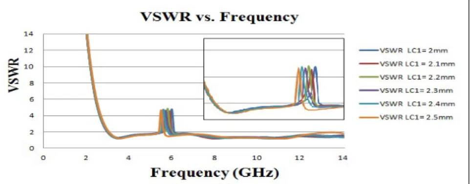
The same parametric analysis is also done on lengths LB1 and LC1 of the slots B and C using Ansoft
HFSS. The VSWR curves for antennas B and C are shown in Fig. 7 and Fig. 8, respectively. It can be observed that the resonance frequencies vary with the slot lengths. So, it can be stated that the notched bands can be individually controlled by their dimensions.
The final optimized dimensions of the slots are provided in Table II.
TABLEII. OPTIMIZED DIMENSIONS OF SLOTS FOR IMPLEMENTING FREQUENCY NOTCHING
Dimensions (mm)
Slot A Slot B Slot C
LA1 = 3.1 mm LB1= 3 mm LC1= 2.3 mm LA2 = 5.1 mm LB2= 3 mm LC2= 2.4 mm LA3 = 13.8 mm LB3= 8.5 mm LC3= 8 mm
TA1= 0.3 mm TB1= 0.3 mm TC1= 0.3 mm TA2= 0.4 mm
TA3= 0.5 mm TB2 = 0.4 mm TC2 = 0.4 mm
Brazilian Microwave and Optoelectronics Society-SBMO received 17 Apr 2018; for review 23 Apr 2018; accepted 7 Nov 2018 Brazilian Society of Electromagnetism-SBMag © 2018 SBMO/SBMag ISSN 2179-1074
By placing different slots on different parts of the patch it is ensured that mutual coupling is reduced to minimum among the different rejection slots. Also, the range of the rejection band can be adjusted by modifying the length of the inserted slot. This property provides us with a huge control to set the notched frequency in our antenna design.
Fig.9 shows the VSWR curves of the individual antennas A, B and C together in one graph. It is also observed that the VWSR values in the rest of the UWB range remains mostly unchanged (VSWR < 2), thereby unaffecting the antenna performance. Table III shows the frequency notch bands achieved by inserting slots A, B and C in the reference antenna. The notches obtained are very narrow and do not waste frequency band.
TABLEIII. INTERFERENCE BANDS CONSIDERED AND NOTCHED FREQUENCY BANDS ACHIEVED FOR PROPOSED TRIPLE BAND NOTCHED UWB ANTENNA
Applications which cause interference
Names of the single notched band antennas designed with their notched frequencies
Respective Bandwidths considered for
notching
Notched bandwidths achieved in the proposed UWB antenna WiMAX Antenna A/slot A 3.3 to 3.7 GHz 3.32 - 3.74 GHz
Lower WLAN Antenna B/slot B 5.15 - 5.35 GHz 5.18 - 5.46 GHz Higher WLAN Antenna C/slot C 5.725 - 5.825 GHz 5.72 - 6 GHz
Fig. 9. Simulated VSWR curves for the single band notched antennas at centre frequencies of 3.5, 5.2 and 5.7 GHz.
Brazilian Microwave and Optoelectronics Society-SBMO received 17 Apr 2018; for review 23 Apr 2018; accepted 7 Nov 2018 Brazilian Society of Electromagnetism-SBMag © 2018 SBMO/SBMag ISSN 2179-1074
III. RESULTS AND DISCUSSION
Fig. 10 shows snapshots of fabricated antennas without notching and with tri-band notching. The antennas are fabricated using the photolithographic technique. A number of sequential steps are involved in this technique. This process is initiated by mask generation, cutting and cleaning of double-sided copper cladded FR4 substrate and application of photoresist coating on substrate. After these steps, the mask is placed on the photoresist coated substrate and exposed to UV light. This step results in hardening of the photoresist material in exposed regions. This is followed by the developing process where the substrate is immersed in developer solution and then dipped in dye solution. At this stage a clear geometry of the antenna design can be viewed on the substrate. After this, the unwanted copper is etched out by dipping the substrate in ferric chloride solution followed by washing in running water to remove any etchant. Finally, the etched substrate with antenna design is cleaned by acetone solution to remove hardened photoresist.
A. Voltage Standing Wave Ratio (VSWR) readings
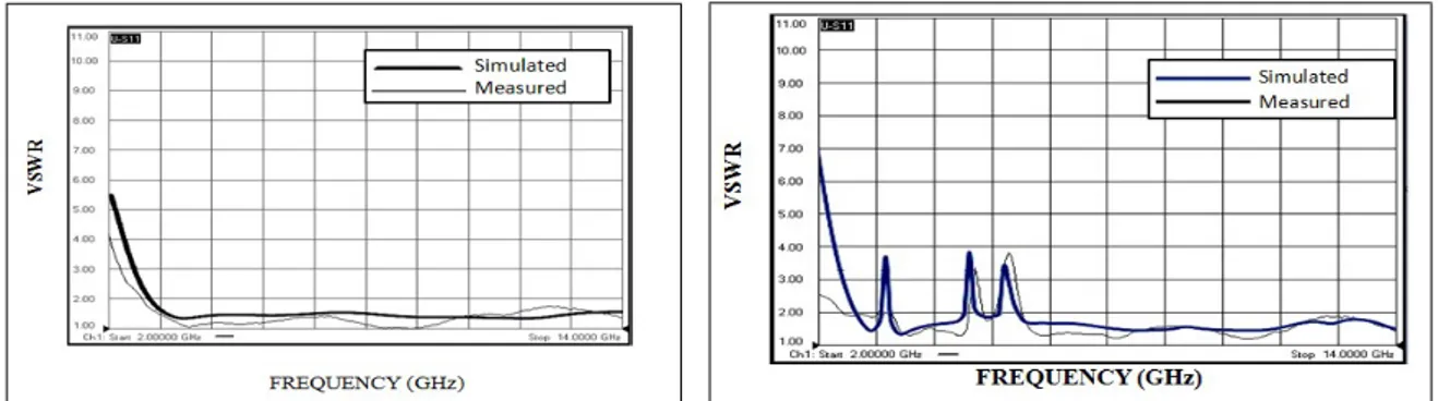
The measurements were done on vector network analyzer (VNA, PNA N5230A, Agilent Technologies). Fig. 11 shows the simulated and measured VSWR curves for the UWB antenna, without slots and with slots. The fabricated antenna achieves a bandwidth of 3.1 to more than 14 GHz successfully with 3 band notches. There are some differences seen in the simulated and measured results. One of the reasons for degradation/discrepancies of antenna performance parameters could be due to fabrication faults and SMA connector which was not used in our simulation.
(a) (b)
Fig. 10. Fabricated Antenna: (a) Without slots and (b) with slots.
(a) (b)
Brazilian Microwave and Optoelectronics Society-SBMO received 17 Apr 2018; for review 23 Apr 2018; accepted 7 Nov 2018 Brazilian Society of Electromagnetism-SBMag © 2018 SBMO/SBMag ISSN 2179-1074
B. Radiation Pattern
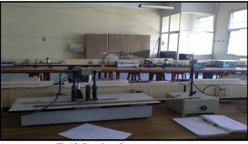
Fig.12 shows the measurement setup used for radiation pattern measurement. C-band (4 GHz - 8 GHz) and X-band (8 GHz - 12.4 GHz) Microwave benches (Vidyut Yantra Udyog [16]) have been used for the purpose. During measurement the proposed UWB antenna is positioned as the receiving antenna on a rotating pedestal. The measured received power is in microwatts (µw) at different angle (θ) values. Thus, the different calculated power points with respect to theta (θ) are used to plot the radiation patterns in E plane and H plane.
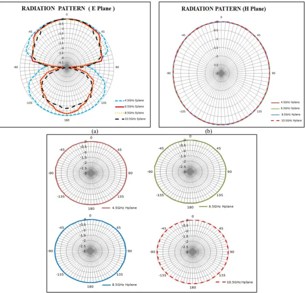
Fig. 13 shows the comparison of simulated E plane and H plane radiation patterns at 4.5, 6.5, 8.5 and 10.5 GHz for the proposed antenna, obtained from the HFSS software. And Fig. 14 shows the comparison of measured E plane and H plane far field patterns of radiation of the proposed antenna at 4.5, 6.5, 8.5 and 10.5 GHz. All the H plane patterns at the respective four frequencies have been plotted individually for more clarity as shown in Fig.14(c). The E plane is an eight-shaped pattern of radiation whereas H plane radiation patterns display almost omni-directional characteristic, which displays monopole like behavior in antenna, quite desirable for mobile applications [9]. However, it is observed that the radiation patterns begin to vary at higher frequencies and more side lobes appear.
(a) (b)
Fig. 13. Simulated Radiation patterns of the proposed band notched UWB antenna at 4.5 GHz, 6.5GHz, at 8.5GHz and at 10.5GHz (a) E plane Radiation patterns (b) H plane Radiation patterns
Brazilian Microwave and Optoelectronics Society-SBMO received 17 Apr 2018; for review 23 Apr 2018; accepted 7 Nov 2018 Brazilian Society of Electromagnetism-SBMag © 2018 SBMO/SBMag ISSN 2179-1074
C. Gain
For UWB antenna it is very difficult to plot radiation patterns at all the frequencies as the operating range is quite large. So, a much more convenient way to visualize and justify the omni-directional pattern is "the gain vs. frequency plot". By observing the gain plot, we can very easily conclude where and at which frequencies the UWB antenna radiates and where it doesn’t radiate at all. This also provides insight into the behaviour of antenna at the notched frequency bands, as it can be clearly seen that antenna doesn’t radiate at the notched bands as shown in Fig. 15. The gain varies from 3.8 dB to 5.9 dB over the operating UWB frequency range except at the filtered bands where a steep decrease in gain is observed as seen in Fig. 15. The peak realized gain is 5.9 dB. The gain is seen to be flat and stable in the overall functional range/un-notched frequency bands, with variations of less than 2.1 dB. This provides further justification that the UWB antenna radiates almost omni-directionally in all directions.
Fig. 15 Realized Peak Gain
(a) (b)
(c)
Fig.14 Measured Radiation patterns of the proposed band notched UWB antenna at 4.5 GHz, 6.5 GHz, at 8.5 GHz and at 10.5 GHz: (a) E plane Radiation patterns, (b) H plane Radiation patterns, (c) Measured H plane radiation
Brazilian Microwave and Optoelectronics Society-SBMO received 17 Apr 2018; for review 23 Apr 2018; accepted 7 Nov 2018 Brazilian Society of Electromagnetism-SBMag © 2018 SBMO/SBMag ISSN 2179-1074
D. Brief study of UWB transmission schemes and Antenna Group Delay
According to "Introduction to Ultra-Wideband Radar Systems" by James D. Taylor [17], over the years, the term ultra-wideband has been called by a number of synonymous terms such as impulse, video pulse, carrier-free, super wideband, non-sinusoidal, baseband, until the US Department of defense used the term Ultra Wideband (UWB) in 1989[17].
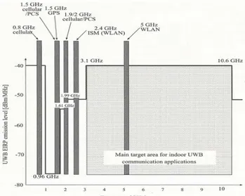
Ultra Wideband by tradition has been accepted as pulse radio. Win and Scholtz described the ultra-wideband pulse-based communication as Impulse Radio UWB (IR-UWB) [18]. The simplest form of IR-UWB uses short timed pulses without a carrier signal to transmit information. And it has to operate under the FCC regulated emission limits for the allocated huge bandwidth of 3.1 GHz - 10.6 GHz [2]. A comparison of UWB bandwidth with other conventional systems is shown below in Fig. 16 [19].
The FCC and ITU-R further introduced the definition of UWB, as signals with fractional bandwidth more than 20% of its central frequency or as signals with bandwidth more than 500 MHz [2], [20]. Therefore, any transmission signal that fulfils the FCC demands for UWB spectrum can be considered UWB technology, i.e., any technology that employs more than 500 MHz bandwidth in the
Brazilian Microwave and Optoelectronics Society-SBMO received 17 Apr 2018; for review 23 Apr 2018; accepted 7 Nov 2018 Brazilian Society of Electromagnetism-SBMag © 2018 SBMO/SBMag ISSN 2179-1074
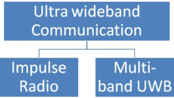
allotted spectral mask having the required emission limits is considered UWB [20]. This definition broadened and included a number of techniques that could be used for UWB implementation which was initially just impulse based. Fig. 17 summarizes the two main techniques used for implementing UWB. The UWB data modulation schemes have been divided into two main categories as seen in Fig. 17: Impulse radio UWB (IR-UWB) and multi-band orthogonal frequency division multiplexing (MB-OFDM). The MB-OFDM format has 14 subintervals in the interval between 3.1 and 10.6 GHz. Each subinterval covers 528 MHz of bandwidth [21].
There are lots of modulation schemes for UWB as shown in Table IV above and many studies have been done and still ongoing in this field because UWB is an evolving technology. Although the work presented in this article primarily deals with the designing of UWB antenna (operating from 3.1GHz - 10.6 GHz) a short and comprehensive idea is tried to be given as to how the research in UWB schemes have evolved and still evolving. For more perceptiveness into the various schemes for UWB, one can refer to [17]-[24].
TABLE IV. UWB MODULATION SCHEMES
UWB COMMUNICATION TYPES:
IR-UWB MB-OFDM
TECHNIQUES FOR TRANSMISSION
THIR-UWB,DSIR-UWB OFDM
MODULATION SCHEMES PPM, PAM, PWM, OOK, BPSK. BPSK,QPSK,PAM,QAM,
FSK.
NATURE OF PULSES VERY NARROW PULSES PULSES NOT VERY NARROW COMPLEXITY SIMPLER CIRCUITRY MUCH MORE COMPLEX
CIRCUITRY
COST MORE ECONOMICAL MORE COSTLY
The focus in this article is to design and develop a workable UWB antenna (operating from 3.1GHz - 10.6 GHz) to study and justify the antenna performance for indoor UWB applications. Therefore, by studying and understanding the functioning and behavior of antenna parameters a much better insight into the designing and development of UWB antennas is acquired.
The numerous advantages of UWB (3.1GHz - 10.6 GHz) for radio communications, like low transmission power, less complex hardware structure and high data throughput rates, compared to
Brazilian Microwave and Optoelectronics Society-SBMO received 17 Apr 2018; for review 23 Apr 2018; accepted 7 Nov 2018 Brazilian Society of Electromagnetism-SBMag © 2018 SBMO/SBMag ISSN 2179-1074
other typical wireless systems present in the market, for dense and crowded areas, has created and sustained the attention around it.
UWB pulse transmission is very useful for high speed data transfer in indoor environments (like homes, offices, malls, stores, medical centers, etc.) where the transmission distances are less. Also, the very short duration UWB pulses have the capacity to penetrate through walls, buildings, plastics, wood etc. and less sensitive to the multipath effect [25].
The study of antennas designed for UWB applications is important and challenging because the UWB antenna can transmit narrow pulses directly, without any filters, inside the allocated UWB band and within the set emission limits, thereby being very economical and simple [2].
As UWB antennas are employed to transmit very narrow pulse signals spread over a large spectrum (several gigahertz), the antenna should be able to radiate a pulse without any distortion, or as little distortion as possible. Therefore, to verify the capability of the proposed antenna to operate as a UWB antenna, it is necessary to achieve a consistent group delay over the entire UWB band [9], [13], [20], [26]. Pulse distortion can be represented by the group delay measurements, thus making this parameter really important.
The group delay is defined as the negative derivative of the phase response (φ) versus frequency (f) [27], [29].
df d d
d
g
2 )
(
(7)
where φ is the far-field phase, and f is the frequency.
The group delay measurement can be very easily done using a conventional vector network analyzer (VNA). Our measurement setup for the group delay consists of two identical antennas, connected to the VNA, placed 30 cm apart and oriented face to face with each other. Fig. 18 (a) shows the measured group delay (graphical representation of (7)) for the reference UWB antenna without the notched bands and the Fig. 18 (b) shows the measured group delay for the proposed tri-band notched UWB antenna. It is seen that group delay varies abruptly at the notched frequency tri-bands and in the un-notched frequency regions the group delay is constant with variation of less than a nanosecond [9], [13], [20].
Brazilian Microwave and Optoelectronics Society-SBMO received 17 Apr 2018; for review 23 Apr 2018; accepted 7 Nov 2018 Brazilian Society of Electromagnetism-SBMag © 2018 SBMO/SBMag ISSN 2179-1074
F. Distribution of Surface Current
The simulated current distributions of the initial antenna geometry before cutting the slots for notching are shown in Fig. 19 (a) and (b), at 4.5GHz and 10.5GHz. It is seen that the current is mainly concentrated on the bottom of the patch with very low density toward and above the center and along the edges of the patch except the top edge, for all frequencies. So, it is clear that the center of the patch which has low current density contributes very little to the antenna performance. Therefore, the notches for mitigating interference can very easily be introduced on the patch without distorting its performance. This is a very attractive feature because of the liberty it presents in designing of the antenna without increasing its complexity or bulkiness. Thus, a more compact and light weight antenna is realized.
Furthermore, in order to understand the effect of slots in getting band notches the surface current distributions on the radiating surface of the proposed antenna are shown at the three centre frequencies of the notched bands in Fig. 20. At notched band frequencies, the concentration of current around the slots is the strongest indicating the notched bands. The current along the edges of the slots is equivalent to the inductor where as the etched slots behave as capacitors for the resonator tank circuits.
(a)
Brazilian Microwave and Optoelectronics Society-SBMO received 17 Apr 2018; for review 23 Apr 2018; accepted 7 Nov 2018 Brazilian Society of Electromagnetism-SBMag © 2018 SBMO/SBMag ISSN 2179-1074
G. Equivalent circuit based on impedance plots
For a narrowband microstrip planar antenna equivalent circuit can be represented by a parallel RLC circuit, based on analysis methods available [14]. But for a UWB planar antenna, a very wide impedance bandwidth (7.5 GHz) has to be taken into account. The UWB antenna is not considered to have a single resonance but multiple overlapping resonances in the entire range of operation. Thus, a UWB antenna's equivalent circuit can be represented as a series of parallel RLC resonators as shown in Fig.21.
For us to draw more physical insight in the behaviour of antenna and notch, simulated impedance curve of triple band notched UWB antenna is shown in Fig. 22.
It is seen that at the first and third notch frequencies of 3.5 GHz and 5.7 GHz, input impedances are akin to that of the series RLC circuit, because the imaginary graph is crossing zero going towards positive value while the real part has a lowest positive value at that point as the real graph moves towards the zero value. And for the second notch frequency of 5.2 GHz a parallel type RLC tank structure is used to represent the band notch structure because a rapid change in the impedance (real and imaginary) is seen here. Thus, the suggested
(a) (b)
(c)
Fig.20. Surface current distributions at the three notched bands. (a) Slot A (3.5 GHz) (b) Slot B (5.2GHz) (c) Slot C (5.7 GHz).
Brazilian Microwave and Optoelectronics Society-SBMO received 17 Apr 2018; for review 23 Apr 2018; accepted 7 Nov 2018 Brazilian Society of Electromagnetism-SBMag © 2018 SBMO/SBMag ISSN 2179-1074 equivalent for the UWB antenna input impedance is expressed as a series of parallel RLC tanks. The band rejection components are expressed with two series RLC tanks connected in shunt with the equivalent antenna and a parallel RLC connected in series with the equivalent antenna as shown in Fig. 23. Thus, the notches behave as band stop filters.
H. Comparison of proposed design with published papers
Table V shows an extensive comparison of the proposed UWB antenna with already published papers of state of the art UWB antennas. It shows that our designed antenna has a very wide bandwidth as well as a very concise size compared to other published designs.
Fig. 22. Impedance curve of Triple band notched antenna.
Brazilian Microwave and Optoelectronics Society-SBMO received 17 Apr 2018; for review 23 Apr 2018; accepted 7 Nov 2018 Brazilian Society of Electromagnetism-SBMag © 2018 SBMO/SBMag ISSN 2179-1074
TABLE V.COMPARISON OF PROPOSED UWB ANTENNA DESIGN WITH ALREADY PUBLISHED PAPERS Published
Papers L x W (mmDimensions: 2) Bandwidth achieved Area (mm
2) No. of Band
rejections obtained
Narrowband Tech. notched
[3] 26 x 30 2.9 - 12.1 GHz 780 Single notch 4.9 - 6 GHz
[4] 63 x 63 3.1 - 10.6 GHz 3969 Single notch 5.1- 6 GHz
[5] 33 x 35.5 2.4 - 11 GHz 1171.50 Dual Notches 5.2 - 5.95 GHz 8.0 - 8.35 GHz
[6] 32 x 26 3 - 11 GHz 832 Single notch 5.0 - 5.9 GHz
[7] 48 x 46 3.1 - 10.6 GHz 2208 Single notch 5.1- 6 GHz [8] 40 x 36 3.8 - 10.8 GHz 1440 Single notch 5 - 6.1 GHz
[9] 28 x 36 2.5 - 11 GHz 1008 Dual Notches 3.3- 3.7 GHz
5.12 - 5.37 GHz [10] 35 x 32 2.6 - 12GHz 1120 Triple Notches 3.3 - 3.6 GHz
5.1 - 5.8 GHz 8.0 - 8.4 GHz [11] 36 x 34 2.9 - 13 GHz 1224 Triple Notches 3.3 - 3.9 GHz 5.2 - 5.35 GHz 5.8 - 6.0 GHz [13] 37 x 34 3.1–10.6 GHz 1258 Dual notches 3.3 - 3.8 GHz 5.1 - 5.9 GHz [27] 30 × 41 3.04 - 10.8 GHz 1230 Dual notches 3.3 - 4.1 GHz 5 – 5.9 GHz [28] 31 x 35 3.05 - 10.94 GHz 1085 Single notch 4.96 - 5.98 GHz
[29] 35 x 65 3.0 - 12 GHz 2275 No notches NA
[30] 26 x 30 2.5 - 25 GHz 780 Dual notches 3 - 3.8 GHz
5.1 - 6.2 GHz [31] 32 x 35 2.6 - 12 GHz 1120 Triple Notches 3.3-3.6 GHz
5.1-5.8 GHz 8.0-8.4 GHz
Proposed
Design 31 x 24 3.1 - 14 GHz 744 Triple notches 3.32 - 3.74 GHz 5.18 - 5.46 GHz
5.72 - 6 GHz
IV.
C
ONCLUSIONThis research paper presents a compact, light weight tri-band notched UWB antenna. The proposed design is simple to design and fabricate and there is a close agreement between simulated and experimentally tested results, in terms of good radiation pattern values and VSWR values ranging between 1 and 2. The strength of this proposal lies in the fact that mutual coupling is reduced to minimum among the different rejection slots due to their placement on the radiator. This approach of introducing the frequency notching slots on the top of antenna patch without affecting the antenna performance provides more degree of freedom in our design development. Also, very narrow notching is obtained thereby not wasting any excess frequency band. An omni-directional radiation characteristic in H-plane further supports the utilization of the designed antenna for WPAN and other UWB applications. Equivalent lumped circuit model is presented which provides a physical insight into the performance of the notch band with respect to the antenna.The proposed scheme could be helpful for designing diverse ultra wideband antennas with outstanding band rejection characteristics.
Brazilian Microwave and Optoelectronics Society-SBMO received 17 Apr 2018; for review 23 Apr 2018; accepted 7 Nov 2018 Brazilian Society of Electromagnetism-SBMag © 2018 SBMO/SBMag ISSN 2179-1074 antennas justifies that the presented antenna is a low cost, compact option for integration in wireless devices.
Thus, the suggested antenna is a fine contender for UWB applications.
ACKNOWLEDGMENT
The authors would like to acknowledge and thank the support of Birla Institute of Technology (Mesra) for providing the facility and equipment for this work.
REFERENCES
[1] "Federal Communications Commission Revision of Part 15 of the Commission’s Rules Regarding Ultra-Wideband Transmission System from 3.1 to 10.6 GHz," in FEDERAL Communications Commission. Washington, DC: ET-Docket, pp. 98–153, FCC, 2002.
[2] H. Schantz, "The Art and Science of Ultra Wideband Antennas", Norwood, MA: Artech House Inc, 2005.
[3] Jaehoon Choi, Kyungho Chung, and Yangwoon Roh," Parametric Analysis of A Band Rejection Antenna For UWB Application”, Microwave And Optical Technology Letters / Vol. 47, No. 3, pp. 287- 290, November 2005.
[4] H-D Chen, Jui-Ni Li, and Y-F Huang,"Band-Notched Ultra-Wide Band Square Slot Antenna", Microwave and Optical
Technology Letters, Vol. 48, No. 12, 2427-2429, December 2006.
[5] Feng-Tao Zha, Shu-Xi Gong, Gang Liu, Hong-Yu Yang, and Shu-Guang Lin," Compact Slot Antenna For 2.4 GHz/UWB With Dual Band-Notched Characteristic", Microwave and Optical Technology Letters, Vol. 51, No. 8, pp. 1859 - 1862, August 2009.
[6] J. Choi, S. Hong, and U. Kim, " The Design of an UWB Antenna with Notch Characteristic", PIERS ONLINE, VOL. 3, No. 7, pp. 987-990, 2007.
[7] F-J. Wang, and J-S Zhang, " Study of A Band-Notched Double Printed Dipole Antenna", Microwave and Optical
Technology Letters, Vol. 50, No. 11, pp. 2986 - 2989, November 2008.
[8] P. Li, L. Ma, and J-S. Li," A Hexagonal Ultra-Wideband Antenna with Notched Band", Microwave and Optical
Technology Letters, Vol. 51, No. 12, pp. 2917 -2921, December 2009.
[9] L. Xie, G. Zhao, Y.-C. Jiao, and F.-S. Zhang," Ultra-Wideband Antenna Using Meandered Slots for Dual Band-Notched Characteristic", Progress In Electromagnetics Research Letters, Vol. 16, pp. 171-180, 2010.
[10]P. Zhuo, H. Tang, X. Gao, F. Zhao and F. Zhang," Investigation on Planar UWB Antenna with Triple Band-Notched Characteristics", iWEM 2012 Proceedings, 978-1-4673-2999-6112/$31.00 ©2012 IEEE.
[11]W. T. Li, X. W. Shi and Y. Q. Hei," Novel Planar UWB Monopole Antenna with Triple Band-Notched Characteristics ", IEEE Antennas and Wireless Propagation Lettters, Vol. 8, pp. 1094-1098, 2009.
[12]L.Y. Cai, G. Zeng, H. C. Yang and X. W. Zhan," Compact printed ultra-wideband antennas with band-notched characteristics", Electronic Letters Vol. 46, No. 12, June 2010.
[13]F. Fan, Z. Yan, T. Zhang, and Y. Song," Ultra-Wideband Planar Monopole Antenna with Dual Stopbands", Microwave
and Optical Technology Letters, Vol. 52, No. 1, pp. 138- 141, January 2010.
[14]C. Balanis Antenna Theory; Analysis and Design (second edition Wiley and Sons, New York) 1982. [15]D. M. Pozar, Microwave Engineering, Third Edition, John Wiley & Sons, 2010.
[16]www.vyu-microwave.com,( microwave components and instrument manufacturers).
[17]J. D. Taylor "Introduction to Ultra-Wideband Radar Systems,.CRC.Press,.Boca.Raton,.FL,1995.
[18]M. Z. Win and R. A. Scholtz," Impulse Radio: How It Works," IEEE Communications Letters, Vol. 2, No. 2, pp. 36 - 38, February 1998.
[19]M. Ghavami, L. B. Michael and R. Kohno, Ultra Wideband Signals and Systems In Communication Engineering, second edition, Wiley, 2007, ISBN 978-0-470-02763-9.
[20]V. S. Padilla," Theoretical Aspects of Ultra Wide Band", Proceedings of the World Congress on Engineering and
Computer Science, Vol I, WCECS 2014, San Francisco, USA, ISBN: 978-988-19252-0-6 , ISSN: 2078-0958 (Print);
ISSN: 2078-0966 (Online), 2014.
[21]C. M. Din, W. Mansor, R. Mohamad," A Review on Modulation Techniques in Multiband Orthogonal Frequency Division Multiplexing in Ultra-Wideband Channel", 2011 IEEE Symposium on Computers & Informatics 978-1-61284-691-0/11/$26.00 ©2011 IEEE,576-582.
[22]T. Ali, P. Siddiqua, M. A. Matin," Performance Evaluation Of Different Modulation Schemes For Ultra Wide Band Systems", Journal of Electrical Engineering, Vol. 65, No. 3, pp. 184–188, 2014.
[23]A. Alarifi, A. Al-Salman, M. Alsaleh, A. Alnafessah, S. Al-Hadhrami, M. A. Al-Ammar and H. S. Al-Khalifa," Ultra Wideband Indoor Positioning Technologies: Analysis and Recent Advances", Sensors, Vol. 16, 707; doi:10.3390/s16050707, pp.1-36, 2016
[24]M. Bali, "Analysis and Future Approach of Ultra Wideband Technology", International Journal of Scientific &
Engineering Research, Vol. 3, No. 4, pp.1-5, April 2012.
[25]S. Ullah, M. Ali, M. A. Hussain and K. S. Kwak, “Applications of UWB technology”, The 5th Annual International
Brazilian Microwave and Optoelectronics Society-SBMO received 17 Apr 2018; for review 23 Apr 2018; accepted 7 Nov 2018 Brazilian Society of Electromagnetism-SBMag © 2018 SBMO/SBMag ISSN 2179-1074
[26]W. Kong, Y. Zhu and G. Wang, "Effects of Pulse Distortion in UWB Radiation on UWB Impulse Communications",
Proceedings of International Conference on Wireless Communications, Networking and Mobile Computing, pp 344-
347, 2005.
[27]S. S. Thwin, Design and Optimization of Integrated Bluetooth And UWB Antenna with Dual Band-Notched Functions", International Journal of Computer Networks & Communications (IJCNC), Vol.4, No.4, pp 251-259. July 2012.
[28]H. Xiao-Xiang, D. Hong-Wei, "New band-notched UWB antenna", J Shanghai Univ., Vol. 13, No. 2, pp. 142–145, Digital Object Identifier (DOI): 10.1007/s11741- 009- 0210, P. R. China, 2009.
[29]Lee, Young-Ki; Hong, Seok-Jin; Kim, Jeong-Pyo; Choi, Jae-Hoon " Design of an Antenna with Near Omni-directional H-Plane Radiation Pattern Over Ultra-Wide Bandwidth". ETRI Journal, Vol. 32, No. 1, pp. 62-67, February 2010. [30]S. R. Emadian, C. Ghobadi, J. Nourinia, M. Mirmozafari, and J. Pourahmadazar," Bandwidth Enhancement of
CPW-Fed Circle-Like Slot Antenna with Dual Band-Notched Characteristic", IEEE Antennas and Wireless propagation
Letters, Vol. 11, pp. 543 - 546, 2012.