A Low-Power Rail-to-Rail Row/Column
Selector Operating at 2 V Using a-IGZO TFTs
for Flexible Displays
Angelo Santos
a, Bhawna Tiwari
b, Jorge Martins
a, Ana Santa
a, Kamal Chapagai
b, Pydi Bahubalindruni
b,
Pedro Barquinha
aa i3N/CENIMAT, Department of Materials Science and Technology,
Universidade NOVA de Lisboa and CEMOP-UNINOVA, Campus de Caparica, 2829-516 Caparica, Portugal. b IIIT-Delhi, Okhla Industrial Estate, Phase III, New Delhi, India - 110020.
Email: bpganga@iiitd.ac.in
Abstract—This paper presents design and implementation of 8-bit shift register with low-voltage amorphous Indium Gallium Zinc Oxide (a-IGZO) thin-film transistors (TFTs) for row/column selection of pixel matrix in flexible dis-plays. This circuit is capable of ensuring complete rail-to-rail operation by employing novel NAND gates that were developed based on capacitive bootstrapping load. As a first step, a positive edge triggered D- flip flop (D-FF) is designed using these logic gates, then a complete 8-bit shift register is designed and simulated using in-house low-voltage IGZO TFT models in Cadence Virtuoso. During these circuit simulations a power supply voltage of 2 V and a channel length of 2 µm were used. Simulation outcome of 8-bit shift register has shown a power consumption of 72.15 µW with output voltage swing of 95% of Vddat 20 kHz
operating frequency, going well beyond the state of the art for oxide TFT technology at very low supply voltage. The proposed circuit can be used as a row/column selector in flexible displays that can operate at low supply voltage and allows small active-area.
Index Terms—IGZO TFTs, pseudo-CMOS, capacitor bootstrapping, shift register, low-voltage operation.
I. INTRODUCTION
A-IGZO TFTs are gaining significant interest in next generation flexible displays [1], as they can be fabricated at low-temperature (typically around 150◦C) [2][3], have high mobility (≈10 cm2/V.s) and stability compared to other TFTs (like a-Si:H, organic). Traditionally, drivers for displays are fabricated using CMOS technology, either using assembled Si chips or on-panel circuitry based on low-temperature poly-Si (LTPS) [4] technology due to high field-effect mobility of charge carriers in comparison to other TFT counterparts, to ensure high speed of operation. However, even for LTPS, fabrication
temperature is typically above 400◦C, due to which
conventional process used for fabricating LTPS TFTs on glass substrate cannot be adopted on flexible substrate [5]. As a consequence, oxide TFTs are preferred choice
for flexible displays in which shift registers are important functional blocks for row/column selection.
The works reported so far on shift registers with oxide TFTs [8]- [11] include a power supply ≥ 8 V and transistor channel length ≥ 10 µm. High operating voltages and large device dimensions of oxide TFTs impose limitation on the implementation of low-power flexible small displays for specific applications, such as, smart-watch displays, micro display applications, pico-projectors etc. with high pixel density. In order to ensure low-power consumption and small area of overall display, it is essential to optimize the power consumption and active area of the display drivers (shift registers). This can be obtained by scaling down the supply voltage and tran-sitor dimensions. On the other hand, oxide TFTs with a channel length ≤ 8 µm show short channel non-idealities, which degrades the circuit performance [12][13]. Re-garding operating voltage of oxide TFTs, it is limited by the rather thick (> 100 nm) and low-k (3.9 for SiO2) insulators typically used when low-temperature fabrication is envisaged. In addition, this technology lacks stable reproducible complementary type device (p-type), hence circuit design has to be accomplished only with n-type transistors.
In order to develop a low-power and miniaturized shift register, this paper proposes an 8-bit shift register that can address all the afore mentioned challenges. The circuit is implemented using cascade stages of positive edge triggered D-FFs, which are designed using NAND gates. With the use of only n-type transistors in NAND gate, complete rail-to-rail operation at the output is quite challenging to achieve. Therefore, novel NAND gate with modified capacitive bootstrapping load has been used in order to ensure complete rail-to-rail operation of 8-bit shift register. Due to low supply voltage (2 V) and small channel length of transistor that were employed in the
circuit (2 µm), the power consumption and active area of the proposed circuit is optimized.
The rest of the paper is organized as follows. Section II gives a brief introduction about low voltage a-IGZO TFT devices and model that is used for designing and simulat-ing the proposed circuits. Section III presents logic gates that were previously reported with only n-type transistors and their limitations. Section IV presents design aspect of novel NAND gate, positive edge triggered D-FF and 8-bit shift register. Section V shows the simulation results of the gates, D-FF and 8-bit shift register at a supply voltage of 2 V, using oxide TFTs with channel length of 2 µm. Finally, section VI draws conclusions.
II. LOWVOLTAGE A-IGZO TFT: FABRICATION,
CHARACTERISTICS ANDMODELING
The staggered bottom-gate a-IGZO TFTs were fabri-cated on a glass substrate in order to extract electrical measurements and create a representative device model. A 60 nm Mo layer was deposited, by means of RF magnetron sputtering, to form gate, source and drain electrodes. A far-ultravoilet assisted process allow
spin-coating of 20 nm thick AlOx dielectric layer, using
combustion synthesis process with a solution based on aluminium nitrate precursor. More details on this insulator can be found in [14]. For patterning layers, optical photolithography and dry (Mo) or wet (IGZO and AlOx) etching processes were used. Finally, all the devices were annealed at 180◦C, in air, for 1 hour.
Fig.1(a) shows SEM image of a-IGZO TFT fabricated with a width and length of 55 µm and 2 µm, respectively. The drain source overlap with the gate is also visible in light shade around the gate metal (∼ 2.5 µm on each side). The effective length of the transistor is shown in the inset. Device measurements (I-V and C-V) have
(a) −1 0 1 2 10−12 10−10 10−8 10−6 10−4 Vgs(V) Id (A) (b)
Fig. 1. Low voltage a-IGZO TFT (a) SEM with width of 55 µm and length 2 µm (b) Transfer Characteristics for Vgs swept from -1 V to
2 V at Vds=2 V.
been carried out under dark at room temperature using a Keysight B1500A semiconductor parameter analyzer and a Cascade EPS-150 microprobe station. The transfer characteristics from the measurement is shown in Fig.1(b)
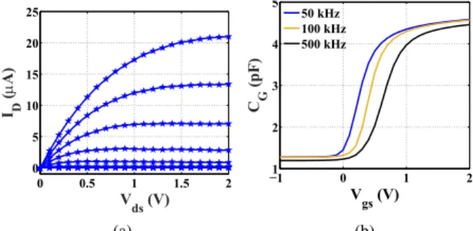
when the gate voltage (Vgs) is swept from -1 V to 2 V with a step size of 0.06 V at Vds= 2 V. The output and C-V characteristics, from measurements, are presented in Fig.2(a) and Fig.2(b), respectively. For the output
0 0.5 1 1.5 2 0 5 10 15 20 25 V ds(V) ID (� A) (a) −11 0 1 2 2 3 4 5 Vgs(V) CG (pF) 50 kHz 100 kHz 500 kHz (b)
Fig. 2. Low voltage a-IGZO TFT (a) Output Characteristics when Vgs
is swept from 0 to 2 V with a step size of 0.25V (b) C-V Characteristics for different frequencies of input signal.
characteristics, Vgsis swept from 0 to 2 V with a step size of 0.25 V. It can be observed from the output chracteristics that the channel length modulation is not siginificant even at a small channel length of 2 µm, unlike other works re-ported in [12][13]. Use of a thin AlOxlayer as a dielectric results in a large gate capacitance (Cox=350 nF/cm2), allowing operation of the transistors at a supply voltage of only 2 V (i.e., transconductance saturation until this voltage). From the measurements, extracted field-effect
mobility is 14 cm2/V.s. The behavioral modelling of
low-voltage a-IGZO TFT, for simulation and designing, is done using artificial neural network based equivalent circuit approach [15] in which parameters extracted from the measurements are used.
III. BASIC LOGIC GATES WITHN-TYPE TRANSISTORS
A. Conventional logic gates
Due to lack of stable complementary type transistor (p-type) with oxide TFTs, circuits need to be designed only with n-type transistors. In this case, the load has to be implemented with either passive resistor (refer Fig.3(a)) or a diode connected transistor (refer Fig.3(b) and Fig.3(c)). Resistive load results in large active area
M1 Vi Vo Vdd R (a) M2 M1 Vi Vo Vdd (b) M2 M1 Vi Vo Vdd (c)
Fig. 3. Inverter with: (a) Resistive Load (b) Diode connected load (c) Zero-bias load.
and high power consumption, therefore, is not a preferred choice for circuit design. The approach of Fig.3(b) results in a threshold voltage drop across the diode load, which in turn limits the output voltage swing and hence, reduces noise margin. Unless M1 is much wider than M2, it is challenging to obtain VOL close to 0 V. The zero-Vgs architecture, in Fig.3(c) with depletion load, can be a so-lution to this problem, but it require extra processing steps to fabricate transistors with different turn-on voltages on the same substrate.
B. Logic gates with Pseudo-CMOS
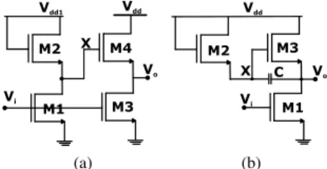
A pseudo-CMOS based circuit presented in [16] is shown in Fig.4(a). It is capable of providing rail-to-rail output voltage with an additional power supply
volt-age source, Vdd1 whose value should not be less than
Vdd + 2Vth. Considering all the transistors in pseudo-CMOS inverter circuit to be identical, the operation of the circuit is as follows: When the input voltage, Vi is low (logic 0), transistor M1 turns off and, therefore, the intermediate node X is charged to Vdd1-Vth which is at-least Vth more than Vdd. As a result, M4 turns on and output voltage, Vopushes to Vdd. On the other hand, when Vi is high, the transistor M1 is on and pulls node X close to logic 0 which turns off M4 while M3 pulls Voto logic 0. Thus, rail-to- rail operation can be observed. The major limitations of this circuit are the need of more than one power supply voltage source and extra area consumption.
X M2 M4 M3 M1 Vi Vo Vdd1 Vdd (a) M2 M3 M1 X C Vdd Vo Vi (b)
Fig. 4. Inverter with: (a) Pseudo CMOS using two different power supplies (b) Bootstrapping Capacitor.
IV. 8-BITSHIFTREGISTER WITHNOVELNAND
GATES
Shift registers are implemented by cascaded stages of positive edge triggered D-FFs, which are designed using NAND gates. Different circuits for logic gates have been reported in previous section, but all have limitations either on electrical response or design/fabrication complexity. In order to have rail-to-rail operation and simplicity at circuit and fabrication level, novel NAND gates designed using a modified version of capacitive bootstrapping load are reported. The details of the design for NAND gates, positive edge triggered D-FF and shift register are discussed next.
A. Logic gates with modified capacitive bootstrapping load
Bootstrapping capacitor, C, in logic gate, (as shown in Fig.4(b)) can shift the voltage level at intermediate node
X, such that, Vdd can be observed at the output when
input voltage is logic 0. Thus, eliminating need of second power supply voltage. However, the circuit is not able to drive output completely to zero, when logic 1 is applied to the input due to finite output impedance offered by M3 at low supply voltages. Therefore, Capacitive bootstrapping circuit is modified by adding a switch, for every input, to the bootstrapping inverter such that node X can be pulled down to zero when logic 1 is applied at the input. This will ensure complete rail-to-rail operation. Each switch in the modified circuit is realized using n-type transistor, like M1, which is shown in Fig.5(a). The same technique can be adapted to other logic gates and a 2-input NAND gate with similar implementation is presented in Fig.5(b). With the optimized fabrication process used in this work, Fig.5(a) resulted in a layout area of 5840 µm2 when C value is 2.5 pF, which is almost 35.47% of area consumed by pseudo CMOS inverter reported in [16].
M2 M4 M1 M3 X C Vdd Vo Vi (a) Vdd Vi1 Vi2 M1 M2 M4 M3 M1' M2' X C Vo (b)
Fig. 5. Logic gates with Modified capacitive bootstrapping load: (a) Invereter: circuit schematic and layout (b) 2-input NAND gate.
B. Positive edge-triggered D Flip-flop
A positive edge triggered D flip-flop (see Fig.6)
Clk D Q Qb Sb Rb Input Output Stage Stage
D-FF1
Clk
Data
Q D Q D D Q D Q D Q D Q D Q D Q D-FF2 D-FF3 D-FF4 D-FF5 D-FF6 D-FF7 D-FF8Q
1Q
2Q
3Q
4Q
5Q
6Q
7Q
8Fig. 7. 8-bit Shift register.
is designed using novel NAND gates whose circuit schematic is presented in Fig.5(b). The operation of the circuit is as follows: The circuit consist of two stages, input and output, implemented by NAND based latches. When the clock (clk) is logic 0, Sband Rbare set to logic 1. Irrespective of the value of D, Q and Qbhold previous state. On the other hand, when the circuit comes across a positive edge of the clk, D value will be transferred to Q.
C. 8-bit Shift register for Flexible Displays
As discussed earlier, shift register plays an important role as a row/column selector in flexible displays. An 8-bit synchronous shift register using positive edge triggered D-FFs is presented in Fig.7. For every positive edge of the clk, the output of the shift register shifts by one bit towards right.
V. RESULTS ANDDISCUSSIONS
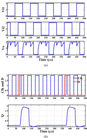
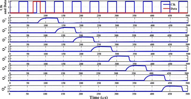
All the circuit simulations are carried out using low voltage in-house models [15] at a supply voltage of 2 V and a transistor channel length of 2 µm, in Cadence Virtuoso. Fig.8(a) shows complete rail-to-rail operation of a 2-input novel NAND gate. Here, the charging and discharging effects at input signals transitions are due to the parasitics of the TFTs. Expected behaviour of positive edge triggered D-FF and 8-bit synchronous shift register can be noticed from Fig.8(b) and Fig.9, respectively. A
VOH of 1.9 V and VOL of 0 V have been achieved for
both circuits. The 8-bit shift register is showing a power consumption of 72.15 µW at 20 kHz operating frequency with a bootstrapping capacitor of 2.5 pF.
Table I summarizes performance metrics of the 8-bit shift register and compares it with state of art work. Compared to other shift registers reported in literature it can be observed that the proposed circuit consumes considerably less power and works with lower supply voltage, without compromising the operating frequency. In addition, the proposed circuit consumes less area compared to state of art work when the comparison is made at inverter level.
0 50 100 150 200 250 300 350 400 450 500 0 1 2 Vi1 0 50 100 150 200 250 300 350 400 450 500 0 1 2 Vi2 0 50 100 150 200 250 300 350 400 450 500 0 1 2 Time (�s) Vo (a) 0 50 100 150 200 250 300 350 400 450 500 0 0.5 1 1.5 2 Clk and D 0 50 100 150 200 250 300 350 400 450 500 0 0.5 1 1.5 2 Time (�s) Q Clk D (b)
Fig. 8. Simulation results of (a) Two input NAND gate. (b) Positive edge-triggered D-FF.
VI. CONCLUSION
This work presented an 8-bit low-power rail-to-rail shift register that is implemented with modified capac-itive bootstrapping load based NAND gates for flexible displays. The circuit design makes use of short channel oxide TFTs with a ultra thin solution processed dielectric. This enables low voltage operation (2 V) and low power consumption (72.15 µW), well beyond the previous re-ports of shift registers with oxide TFTs. This circuit finds potential application in low-power flexible displays with high pixel density, without requiring temperatures above
0 50 100 150 200 250 300 350 400 450 500 0 1 2 Clk and Data 0 50 100 150 200 250 300 350 400 450 500 0 1 2 Q 1 0 50 100 150 200 250 300 350 400 450 500 0 1 2 Q 2 0 50 100 150 200 250 300 350 400 450 500 0 1 2 Q 3 0 50 100 150 200 250 300 350 400 450 500 0 1 2 Q 4 0 50 100 150 200 250 300 350 400 450 500 0 1 2 Q 5 0 50 100 150 200 250 300 350 400 450 500 0 1 2 Q 6 0 50 100 150 200 250 300 350 400 450 500 0 1 2 Q 7 0 50 100 150 200 250 300 350 400 450 500 0 1 2 Time (�s) Q 8 Clk Data
Fig. 9. Transient simulation of 8-bit shift register. TABLE I
PERFORMANCE COMPARISON OF STATE OF THE ART SHIFT REGISTERS USING OXIDETFTS Parameters [6] [7] [8] [9] [10] [11] This work
Supply Voltage, Vdd(V) 20 20 30 2 26 ≥ 20 2
Operating Frequency (kHz) 40 13.9 13.2 5 22.1 upto 0.24 20
Device Channel Length (µm) 10 10 10 10 11 11 2
Power Consumption (µW) - 1670 3800 - - - 72.15
180◦C for fabrication.
ACKNOWLEDGMENT
This work is supported by early career research grant with project ref. ECR/2017/000931. This work is also funded by FEDER funds through the COMPETE 2020 Programme and National Funds through FCT - Por-tuguese Foundation for Science and Technology under the project number POCI-01-0145-FEDER-007688, Ref-erence UID/CTM/50025 and the doctoral grant research number SFRH/BD/122286/2016. This work also received funding from the European Communitys H2020 pro-gram under grant agreement No. 716510 (ERC-2016-STG TREND) and No. 692373 (BET-EU). This article is also a result of the project ORABAC/17852, supported by Lisbon Regional Operational Programme (Lisboa 2020) and Alentejo Regional Operational Programme (Alentejo 2020), under the PORTUGAL 2020 Partnership Agree-ment, through the European Regional Development Fund (ERDF)
REFERENCES
[1] J.-h. Lee, D.-h. Kim, D.-j. Yang, S.-y. Hong, K.-s. Yoon, P.-s. Hong, C.-o. Jeong, H.-S. Park, S. Y. Kim, S. K. Lim, S. S. Kim, K.-s. Son, T.-K.-s. Kim, J.-y. Kwon, and S.-y. Lee , “42.2: World’s
Largest (15-inch) XGA AMLCD Panel Using IGZO Oxide TFT,” SID Symposium Digest of Technical Papers, Vol. 39: pp. 625628. doi:10.1889/1.3069740. May. 2008.
[2] E. Fortunato, P. Barquinha, A. Pimentel, A. Goncalves, A. Marques, R. Martins, and L. Pereira, “Wide-bandgap high mobility ZnO thin-film transistors produced at room temperature,” Appl, phys. lett., vol. 85, no. 13, pp.2541-2543, Sep. 2004.
[3] T. Kamiya, K. Nomura, H. Hosono, “Present status of amorphous InGaZnO thin-film transistors,” Sci. Technol. Adv. Mater., vol. 11, no. 4, Sep. 2010, Art. no. 044305.
[4] M. Takabatake, J. Ohwada, Y. A. Ono, K. Ono, A. Mimura and N. Konishi, “CMOS circuits for peripheral circuit integrated poly-Si TFT LCD fabricated at low temperature below 600C,” in IEEE Transactions on Electron Devices, vol. 38, no. 6, pp. 1303-1309, Jun 1991.
[5] X. Gao, L. Lin, Y. Liu and X. Huang, “LTPS TFT Process on Polyimide Substrate for Flexible AMOLED,” in Journal of Display Technology, vol. 11, no. 8, pp. 666-669, Aug. 2015.
[6] A. Jamshidi-Roudbari, S. Akbar Khan and M. K. Hatalis, “High-Frequency Half-Bit Shift Register With Amorphous-Oxide TFT,” IEEE Electron Device Letters, vol. 31, no. 4, pp. 320-322, April 2010.
[7] B. Kim et al., “A Depletion-Mode a-IGZO TFT Shift Register With a Single Low-Voltage-Level Power Signal,” IEEE Electron Device Letters, vol. 32, no. 8, pp. 1092-1094, Aug. 2011.
[8] B. Kim, C.-I. Ryoo, S.-J. Kim, J.-U. Bae, H.-S. Seo, C.-D. Kim, and M.-K. H, “New Depletion-Mode IGZO TFT Shift Register,” IEEE Electron device letters, vol. 32, no. 2, Feb. 2011.
[9] D. Geng, D. H. Kang, M. J. Seok, M. Mativenga and J. Jang, “High-Speed and Low-Voltage-Driven Shift Register With Self-Aligned Coplanar a-IGZO TFTs,” IEEE Electron Device Letters,
vol. 33, no. 7, pp. 1012-1014, July 2012.
[10] H. Jeong, B. K. Choi, H. J. Chung, S. G. Lee, Y. M. Ha and J. Jang, “Long Life-Time Amorphous-InGaZnO TFT-Based Shift Register Using a Reset Clock Signal,” IEEE Electron Device Letters, vol. 35, no. 8, pp. 844-846, Aug. 2014.
[11] E. Song, B. Kang, I. Han, K. Oh, B. Kim and H. Nam,“Depletion Mode Oxide TFT Shift Register for Variable Frame Rate AMOLED Displays,” IEEE Electron Device Letters, vol. 36, no. 3, pp. 247-249, March 2015.
[12] P. G. Bahubalindruni et al., “Influence of Channel Length Scaling on InGaZnO TFTs Characteristics: Unity Current-Gain Cutoff Frequency, Intrinsic Voltage-Gain, and On-Resistance,” in Journal of Display Technology, vol. 12, no. 6, pp. 515-518, June 2016. [13] J. Raja, K. Jang, C. P. T. Nguyen, N. Balaji, S. ‘Chatterjee and
J. Yi, “Drain-Induced Barrier Lowering and Parasitic Resistance Induced Instabilities in Short-Channel InSnZnO TFTs,” in IEEE Electron Device Letters, vol. 35, no. 7, pp. 756-758, July 2014. [14] E. Carlos, R. Branquinho, A. Kiazadeh, P. Barquinha, R.
Mar-tins, and E. Fortunato, “UV-Mediated Photochemical Treatment for Low-Temperature Oxide-Based Thin-Film Transistors,” in ACS Applied Materials and Interfaces, vol. 8, pp. 31100-31108, 2016. [15] G. Bahubalindruni, V. G. Tavares, P. Barquinha, P. G. Oliveira,
R. Martins, and E. Fortunato, “InGaZnO TFT behavioral model for IC design,” Analog Integrated Circuits and Signal Processing, Issue. 1, vol. 87, pp. 73-80, Apr. 2016.
[16] T. C. Huang et al., ”Pseudo-CMOS: A Design Style for Low-Cost and Robust Flexible Electronics,” in IEEE Transactions on Electron Devices, vol. 58, no. 1, pp. 141-150, Jan. 2011.
[17] J. W. Choi, J. I. Kim, S. H.Kim, and J. Jang, “Highly Reliable Amorphous Silicon Gate Driver Using Stable Center-Offset Thin-Film Transistors,” IEEE transactions on electron devices, vol. 57, no. 9, Sep. 2010.
[18] D. Geng, Y. F. Chen, M. Mativenga, and J. Jang, “30 m-Pitch Oxide TFT-Based Gate Driver Design for Small-Size, High-Resolution, and Narrow-Bezel Displays,” IEEE electron device letters, vol. 36, no. 8, Aug. 2015.