Ana Cecilia Marques de Beaumont
Bachelor of Science in Micro and Nanotechnologies Engineering
ZTO Thin film transistor parameter extraction and
modeling
Dissertation submitted in partial fulfillment of the requirements for the degree of
Master of Science in
Micro and Nanotechnologies Engineering
Supervisor: Dr. Arokia Nathan, Full Professor,
University of Cambridge
Co-supervisor: Dr. Pedro Barquinha, Assistant Professor,
Faculdade de Ciências e Tecnologia
da Universidade Nova de Lisboa
ZTO Thin film transistor parameter extraction and modeling
Copyright © Ana Cecilia Marques de Beaumont, Faculdade de Ciências e Tecnologia, Universi-dade NOVA de Lisboa.
A Faculty of Sciences and Technology e a NOVA University of Lisbon têm o direito, perpétuo e sem limites geográficos, de arquivar e publicar esta dissertação através de exemplares impres-sos reproduzidos em papel ou de forma digital, ou por qualquer outro meio conhecido ou que venha a ser inventado, e de a divulgar através de repositórios científicos e de admitir a sua cópia e distribuição com objetivos educacionais ou de investigação, não comerciais, desde que seja dado crédito ao autor e editor.
Acknowledgements
This thesis is the culminate of a long journey that was only possible due to the contribute of all the people that supported me during the last years.
I would firstly like to thank Professor Rodrigo Martins and Professor Elvira Fortunato for creating the Micro and Nano Engineering degree, without it I would not be pursuing my higher education and developing my skills in such a place of excellence that is the NOVA University.
I would like to thank the University of Cambridge and my supervisor Professor Arokia Nathan, for suggesting this theme and allowing me to have this great opportunity of developing research abroad in the scope of the BET-EU project.
I would like to thank Dr. Xiang Chen for working closely with me, for teaching me all the aspects of modelling and helping whenever I felt a bit lost.
I would also like to thank my co-supervisor Pedro Barquinha, for supporting me and con-tributing to the completion of this thesis.
Agradeço aos meus pais, por todo o apoio que me têem dado ao longo destes anos, mesmo quando desesperava e me fechava no quarto a stressar, tanta a paciência e amor que me têem dado.
À minha irmã, especialmente nesta última fase tem sido a mais fofinha, e até meu irmão que às vezes até é fixe, mas tem que ter mais juízo.
Agradeço à minha melhor amiga, Isabel, sempre esteve lá para mim para me mandar «ir trabalhar», dar conselhos e visitar-me quando tive saudades!
Obrigado ao Jolu, sem ti de certeza que não estaria tão bem. Nem sei bem como descrever todo o apoio que me tens dado, mas gosto mesmo muito de ti.
Obrigado à Daniela, por me ajudar tanto mas tanto na realização desta tese, não só pela ajuda em formatação mas também pela calma e apoio nas últimas horas!
Obrigado ao Fernocas, por tantas conversas no hangouts e ajuda no Latex, por apoio e por todas as parvoíces.
Obrigado aos meus colegas de casa, Shiv, Joana e Crespo, por todo o companheirismo e discussões de ideias que me ajudaram durante a realização deste trabalho.
Obrigado aos meus colegas aqui do CENIMAT, Marco, Inês, Cátia por me ajudarem quando voltei na utilização das máquinas, na troca de ideias, na ajuda preciosa na escrita! Ao Saraiva, obrigada por toda a ajuda, especialmente nos gráficos quando estava a dar em louca. Ao Tiggus por ainda tentar fazer com que as minhas ideias malucas resultassem. À Samouco, pelo apoio de último minuto quando pensava que nada podia correr pior. E a todas as outras pessoas que não mencionei mas da sua maneira me apoiaram e me ofereceram um ombro amigo.
Abstract
Transistor models are of utmost importance for device behaviour prediction and circuit de-sign. Physical modelling has the advantage of the parameters being correlated based on device physics. This allows to gain insight on the device during the analysis and extraction of param-eters phase. However, the extraction methods may not consider possible non-idealities of the device, which can cause modelling issues when working with novel thin film transistors (TFTs).
A simple physical DC and AC model was applied to a novel zinc tin oxide TFT annealed at low temperatures (200 ºC). The characteristic curves of four devices with different dimensions
were measured and analysed, and the model parameters were extracted. The characterization and optimization of the models were implemented through the analysis of the fitting with the measured data. Two DC models were developed, the main difference being the contact
resis-tance extraction - using the classic transmission-line method or a procedure based on MOSFETs with non-ideal behaviour that considers the possible bias dependency of the parameter. The latter method allowed to simulate the device characteristic curves more effectively. The AC
model did not fit for frequencies above the cut-offand differed slightly for lower frequencies
due to the simplicity of the model applied.
Keywords: Semiconductor device modeling, Thin film transistors,Parameter extraction, Con-tact resistance
Resumo
Os modelos de transístor são de extrema importância para a previsão do comportamento dos dispositivos e design de circuitos. Os modelos físicos possuem a vantagem de existir uma correlação entre os parâmetros extraídos e a física por detrás do dispositivo. É possível assim obter informações sobre o transístor durante a fase inicial de extração de parâmetros. No en-tanto, os métodos de extração podem não considerar possíveis não-idealidades do dispositivo, o que pode levar a erros durante a criação do modelo para novos transístores.
Um modelo físico DC e um modelo físico AC foram aplicados a transístor de filme fino de ZTO recozido a baixas temperaturas (200 ºC). As curvas características de quatro dispositivos com diferentes dimensões foram medidas e analisadas, e os parâmetros do modelo DC foram extraídos. A caracterização e otimização dos modelos foram implementadas através da análise da comparação com os dados medidos. Foram desenvolvidos dois modelos DC, sendo a prin-cipal diferença o método de extração de resistência de contato - usando o método de linha de transmissão clássico ou um procedimento baseado em MOSFETs com comportamento não ideal, que considera a possível dependência do parâmetro em valores de tensão aplicados. O último método permitiu simular as curvas características do dispositivo de forma mais eficaz. O mo-delo AC não se adequava às frequências acima do corte e diferiu ligeiramente para frequências mais baixas devido à simplicidade do modelo aplicado.
Palavras-chave: Modelização de dispositivos semicondutores, Transístor de filme fino, Extração de parâmetros, Resistência de contacto
Contents
List of Figures xv
List of Tables xvii
List of symbols xix
Acronyms xxi
Objective xxiii
1 Introduction 1
1.1 Thin film transistor . . . 1
1.1.1 Device structure and behaviour . . . 1
1.1.2 Materials and production techniques . . . 2
1.2 Device Modeling . . . 3
1.2.1 DC Model . . . 3
1.2.2 AC Model . . . 4
1.2.3 S Parameters . . . 5
1.2.4 Unity gain cut offfrequency . . . 5
2 Methodology 7 2.1 Parameter Extraction Methods . . . 7
2.1.1 DC Measurement . . . 7
2.1.2 Transconductance extraction . . . 9
2.1.3 Capacitance-Voltage Measurement . . . 9
2.1.4 AC Measurement . . . 10
3 Analysis of Results 11 3.1 DC Model . . . 11
3.1.1 Threshold voltage . . . 11
3.1.2 Contact resistance . . . 12
3.1.3 Power parameter . . . 12
3.1.4 Transconductance parameter . . . 12
3.1.5 Channel length modulation parameter . . . 13
3.1.6 Saturation parameter . . . 14
3.1.7 Model fitting . . . 14
3.1.8 Bias dependent parameters . . . 16
3.1.9 Second Model fitting . . . 18
3.2 AC Model . . . 20
3.2.1 Transconductance . . . 20
3.2.2 Dielectric and overlap capacitance . . . 21
3.2.3 S parameters fitting . . . 22
C O N T E N T S
3.2.4 Current Gain . . . 26
4 Conclusion and future perspectives 29
Bibliography 31
A Appendix 1 35
A.0.1 S Parameter equations . . . 35 A.0.2 Current gain . . . 35
B Appendix 2 37
B.1 Matlab scripts for Model . . . 37 B.1.1 DC Model . . . 37 B.1.2 AC Model . . . 39
C Appendix 3 43
C.1 Optical microscope images . . . 43
I Annex 1 45
List of Figures
1.1 TFT architectures a)Top gate; staggered b)Bottom gate; staggered c)Top gate;
copla-nar d)Bottom gate; coplacopla-nar . . . 1
1.2 Zinc tin oxide TFT structure and materials . . . 2
1.3 TFT structure with contact resistance . . . 4
1.4 FET small signal model circuit for high frequencies . . . 4
1.5 Block diagram of a 2-port network . . . 5
1.6 Transition frequency of a MOSFET . . . 5
2.1 Rtot vsLplot for contact resistance extraction method . . . 7
2.2 Gate-source capacitance example . . . 10
3.1 Methods of threshold voltage extraction . . . 11
3.2 Contact resistance extraction . . . 12
3.3 Linear fitting ofIDS/gmlin versusVGS-VT for a transistor with dimensions W=20 µm and L=40µm . . . 13
3.4 Linear fitting of m to the power of−α1−1 in function ofVGS-VT . . . 13
3.5 Linear fitting of saturation region for the output curves of a transistor with dimen-sions W and L equal to 20µm . . . 14
3.6 Linear fitting of (IDSlinWL) 1 α in function ofVGSfor a transistor with dimensions W=20 µm ans L=160µm . . . 15
3.7 Linear fitting of model with VGS dependent contact resistance and∆L for applied VDS of 5 mV . . . 16
3.8 Linear fitting of model withVGS dependent contact resistance and∆L for applied VDS of 10 V . . . 17
3.9 Linear fitting of model withVGS dependent contact resistance and∆L for applied VDS of 100 mV . . . 18
3.10 Linear fitting of model withVGS dependent contact resistance and∆L for applied VDS of 100 mV . . . 19
3.11 Linear fitting of lower mobility model withVGS dependent contact resistance and ∆L for appliedVDSof 100 mV . . . 19
3.12 Plot of saturation mobility versusVGS for a transistor with W=20µm and L=80µm with an appliedVDS of 10 V . . . 20
3.13 IDS and first derivative ofIDS in function ofVGS with appliedVDS of 10 V for gm extraction . . . 21
3.14 Capacitance measurement for transistor with dimension 160/20µm . . . 21
3.15 Fitting of S11magnitude . . . 22
3.16 Fitting of S11phase . . . 23
3.17 Fitting of S11data with function . . . 23
3.18 Fitting of S21magnitude . . . 24
3.19 Fitting of S21phase . . . 25
L i s t o f F i g u r e s
3.20 Fitting of S22magnitude . . . 25
3.21 Fitting of S22phase . . . 26
3.22 Fitting of h21 . . . 27
3.23 h21approximation comparisons . . . 27
C.1 Image extracted from the optic microscope, with a scale of 100µm, of the thin film transistor channel with dimensions W=20µm and L=160µm . . . 43
C.2 Image extracted from the optic microscope, with a scale of 100µm, of the thin film transistor channel with dimensions W=20µm and L=80µm . . . 43
C.3 Image extracted from the optic microscope, with a scale of 100µm, of the thin film transistor channel with dimensions W=20µm and L=40µm . . . 44
C.4 Image extracted from the optic microscope, with a scale of 100µm, of the thin film transistor channel with dimensions W=20µm and L=20µm . . . 44
List of Tables
3.1 ObtainedVAvalues for all the appliedVGS curves . . . 14
3.2 Extracted parameters summary. . . 15
3.3 Extracted parameters summary. . . 17
3.4 Extracted parameters summary. . . 18
3.5 High frequency parameters summary. . . 22
List of symbols
κ Dielectric constant.
α Power parameter.
λ Channel length modulation parameter.
∆L Channel length modulation parameter.
µeff Transistor channel mobility. Ai Transistor current gain.
Ci Gate dielectric capacitance per area.
Cch Gate/channel Capacitance.
Covd Drain overlap capacitance.
Covs Source overlap capacitance.
fT Frequency at which the modulus of the short circuit current gain is unity.
gm Transconductance.
IDS Drain-source current.
K Transconductance parameter.
L Transistor channel length.
poly-Si Poly-Silicon.
RD Parasitic resistance on the drain contact of the transistor.
RDS Parasitic resistance on the source and drain contacts of the transistor.
RS Parasitic resistance on the source contact of the transistor.
S Parameters Scattering parameters; a type of high frequency parameters used to describe circuits in terms of wave propagation.
VDS Drain-source voltage.
VGS Gate-source voltage.
VT Threshold voltage.
VA Early Voltage.
L I S T O F S Y M B O L S
W Transistor channel width.
z0 Characteristic impedance of a line.
Acronyms
AC Alternating Current.
DC Direct Current.
IGZO Indium Gallium Zinc Oxide.
MOSFET Metal Oxide Field Effect Transistor.
TFT Thin Film Transistor.
ZTO Zinc Tin Oxide.
Objective
This project was realized at the University of Cambridge, in collaboration with CENIMAT in the scope of the BET-EU european project (grant agreement 692373). The main aim of this project is to analyse and apply a physical model to a zinc tin oxide thin film transistor. Transistor models are of utmost importance as they allow us to predict the behaviour of a device, and are necessary to the design of complex circuits. By studying the parameters and the fitting of a physical model to the device we can gain insight to physical phenomena happening within a transistor. The proposed objectives for the thesis are the following:
1. Perform electrical measurements on the fabricated TFTs, regarding capacitance-voltage, transfer and output-voltage characteristics;
2. Obtain a full set of device parameters needed for the compact TFT modeling, using the aforementioned measurements;
3. Apply the parameters to the physical models (both large-signal and small-signal);
4. Optimize the model fitting on the transistor’s characteristic curves and analyse the fitted parameters.
1
Introduction
1.1 Thin film transistor
The thin film transistor (TFT) is a field effect transistor that operates on the same basic
princi-ples as the metal oxide field effect transistor (MOSFET). It is a device with three terminals (gate,
source and drain) made by depositing thin films in a wafer independent substrate. Regarding its structure, the main difference between the TFT and the MOSFET relies on the substrate; the
former uses mainly non-conducting substrates such as glass, and the latter uses semiconductor substrates such as a silicon wafer. The use of glass as a substrate presents advantages such as transparency and low transmission of liquid and vapor water [1] (which prevents damage to the device) making TFTs very useful for their application in display technology. Presently, the use of flexible displays is shifting the attention from glass to polymeric substrates, and new ap-plications of TFTs in wearable devices, sensors and biomedical systems are being developed[2, 3, 4].
1.1.1 Device structure and behaviour
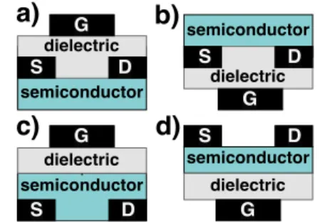
Figure 1.1: TFT architectures a)Top gate;
staggered b)Bottom gate; staggered c)Top gate; coplanar d)Bottom gate; coplanar
The basic TFT consists of a semiconductor active layer, a dielectric and three electrodes named source, drain and gate. Various structures can be arranged (Figure 1.1) depending on the position of the source and drain contacts relative to the gate (top or bottom gate) and the semiconductor layer (staggered when separated by the semiconductor layer, coplanar when on the same side).[5]
The TFT operates identically to the MOSFET in the manner that a tension applied to the gate will turn the device on or off, controlling the current flow between the source and drain
electrodes. Depending on the threshold voltage (VT) needed for the device to function, a TFT
can be defined as an enhancement-mode device (for N-type if VT>0) or as an depletion-mode
device (for N-type if VT<0). Ideally it will act like a capacitor where the charges accumulate at
the interface between the semiconductor and dielectric when a certain gate bias is applied. The differences start in the operation zone, as the TFT operates in the accumulation
condi-tion while a MOSFET operates normally in the inversion. The operacondi-tion zone is reflected in the current flow as the conduction channel is created by the accumulation of majority carriers. This means that there is no inversion in the polarity of induced carriers, which creates difficulty in
defining the accumulation threshold.[6] The disorder of the semiconductor channel layer also creates difficulty in perceiving the VT, due to the existence of localized deep and shallow traps
in the band-gap. The density of carriers trapped in those states can be superior to the density of free carriers, which means that the trap states determine the behaviour of field-effect mobility
as a function of gate bias.[6]The absence of a depletion region is another distinction from the MOSFET, as the TFT device is not isolated from the substrate nor has a p-n junction near the contact preventing the current flow before the channel formation.
C H A P T E R 1 . I N T R O D U C T I O N
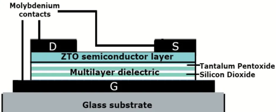
Figure 1.2:Zinc tin oxide TFT structure and materials
1.1.2 Materials and production techniques
TFTs with an amourphous silicon active layer are the most commonly fabricated in large scale electronics due to its low cost. However other types of materials as the higher mobility polycristalline silicon(poly-Si), metallic oxides and organic semiconductors are also used when fabricating TFTs. There is a strong interest in oxide TFTs as they have shown to possess high transparency, good environmental stability, reproducibility and can exhibit mobilities compa-rable to poly-Si.[7, 8, 9] . That interest started predominantly for Indium Gallium Zinc Oxide (IGZO), and since 2012 has been observed the commercialization of products containing this material.Yet, due to the scarcity of gallium and indium, the costs related to this oxide are subject to increases. This stimulated the search for a substitute. Amongst the different oxide materials
investigated, Zinc Tin Oxide (ZTO) has shown to be a possible alternative to IGZO, as tin is an abundant and inexpensive metal that has a similar electronic configuration to indium. The low cost and high transparency of ZTO (due to the high optical band gap) and the possibility of an environmentally friendly deposition process make it an attractive replacement. [7]
The materials used in the thin film transistor dielectric are normally insulating materials with high values of dielectric constant (high-κ) in order to obtain a higher gate capacitance with miniaturization.[10] The issue with high-κ materials is that they may exhibit a low bandgap energy which can allow for electrons to tunnel across the dielectric. This can be solved with the use of a multilayer dielectric, for example, that combines the high-κmaterial with silicon oxide, limiting the leakage and still obtaining a good capacitance value.[11]
The device used in this project is a vacuum-processed NMOS ZTO TFT with a multilayer TaO5/SiO2 dielectric in a corning glass substrate (Figure 1.2) annealed at 200◦C. A higher
annealing temperature would have a reduction effect on the deep and shallow states due to
the decrease of intrinsic defects such as oxygen vacancies, thereby making the device more stable.[12] However, a lower temperature of annealing is preferred as it allows for a lower cost of fabrication and possible use on flexible electronic applications. Nevertheless, the non-ideal behaviour of the device creates a significant need for models capable of interpreting its performance.
1 . 2 . D E V I C E M O D E L I N G
1.2 Device Modeling
Device modeling plays a crucial role in today’s method of representing and analysing the operation of electronic devices. Compact models able to be applied in circuit simulating soft-ware are needed in order to simulate and predict the behaviour of devices in circuits or more complex systems. As the complexity of solid state devices increases, the search for simple mod-els that can provide a good approximation to the device operation while taking into account the various special physical phenomena and non-linear behaviour becomes more necessary. We can consider three different categories of semiconductor device models:
• Physical - Provides physical insight to the performance properties, allowing to predict the behaviour even when exists parameter variation. But it may fail for devices where there is lack of information about the phenomena governing processes;[13]
• Empirical - Computational model that can often give reasonable results for devices with no prior experimental data. However is only based on fitted data, being difficult to
extrap-olate to other devices or dimensions;
• Semi-Empirical - Calculated with adjustable parameters fitted to experiments or first-principles calculations.[13]
In the following parts of the project the physical model will be the adopted model type.
1.2.1 DC Model
A DC Model is a numerical relation that relates the terminal voltages to the currents of the device at dc and low frequencies.[14]In the case of N-type MOSFET devices, we can write the drain-source current (IDS) as a function of the voltages between the gate and source (VGS) and
the source and drain (VDS) using the equations[15]:
IDS =
Subthreshold Current VGS < VT Subthreshold region (1.1a) µeffCi
W
L [(VGS−VT)VDS−V
2
DS] VDS < VGS> VT Linear region (1.1b)
1 2µeffCi
W
L [VGS−VT]
2 V
DS > VGS> VT Saturation region (1.1c)
Where W represents the channel width, L the channel length, µeff the channel mobility, Ci the gate dielectric capacitance per area, VTthe threshold voltage.µeffCican also be represented
by the transconductance parameter (K).
On TFTs we can observe the presence of a various effects, due to special physical phenomena
or bias and geometry dependence of parameters, that are not included in the ideal transistor model and that should be described.
1.2.1.1 TFT model
One of the differences that make the MOSFET model unable to interpret the TFT behaviour
is the effect of the often nonlinear series resistance (RDS). This parasitic resistance is mainly
due to the regions connecting the metal contacts of the source and drain to the transistor channel.[16] The influence is especially observed in small channel devices, where the device’s transconductance does not increase as expected when the channel length (and therefore the
C H A P T E R 1 . I N T R O D U C T I O N
channel resistance) is reduced. The voltage on the internal terminals of the TFT is significantly less than the voltage applied to the drain and source contacts . This is due to the voltage drop on the contact resistance. [17] We can observe in Figure 1.3 the TFT structure of the model including the intrinsic TFT and contact resistances.
Figure 1.3: TFT
struc-ture with contact resis-tance
The voltagesVD′andVS′ control the current in the channel, and relate to it and the contact resistance by the equations [18]:
VGS′ =VGS−IDS.RS=VGS−IDSR2DS (1.2)
VDS′ =VDS−IDS(RS+RD) =VDS−IDSRDS (1.3)
Being that the previous equations are only correct if we assume the symmetry of the device (in other words RDS=RD+RS).
According to the model of Servati et al.(2003), we can represent the above threshold behaviour of a TFT considering the contact re-sistance, the IDS carrier velocity saturation that has a dependence on the VGS voltage [15] and other non-ideal effects. The power
param-eter (α) relates to the carrier velocity saturation effect, which could
lead to inaccuracies if it was assumed to be two like in MOSFET devices. The model is described by the following equations [18]:
IDS=
K W
Lef f(VGS−VT−
VDS
2 )α−
1(V
DS−IDSRDS) Lin. (1.4a)
K α
W Lef f γsat
[(VGS−IDSR2DS −VT)αxcm Sat. (1.4b)
Where xcm is a variable dependent on VDS that incorporates the channel length modulation parameter on the equation,γsatis the current saturation parameter, Lef f is the effective channel
length and K (equation 1.5) is provided unit matching by the parameterζ.
K=µeffζCiα−1 (1.5)
1.2.2 AC Model
1.2.2.1 MOSFET small signal model
The small signal model provides information about the ratio of small perturbations of the large-signal variables. Standard equivalent circuit models for FET devices are well established, being the hybrid-pi model the most used. However, the MOSFET hybrid-pi model does not take into account the contact parasitic resistances that affect TFTs, which may cause some
inaccuracies especially in cases of high RDSvalues.[19]
Figure 1.4:FET small signal model circuit for high frequencies
1 . 2 . D E V I C E M O D E L I N G
Figure 1.4 displays the MOSFET model adapted for high frequencies with added capaci-tances, where Covs and Covd are equivalent to the overlap capacities of the source and drain respectively and Cch to the channel capacitance. The term gm stands for the device transcon-ductance and z0is in general an arbitrary reference impedance, but usually the characteristic
impedance of a line 50Ω.
1.2.3 S Parameters
The S Parameters (scattering parameters) are a type of high frequency parameters used to describe circuits in terms of wave propagation. They relate incident waves to transmitted and reflected ones, simplifying the circuit analysis. A TFT can be analysed as a 2 port network (Figure 1.5) from which we can obtain the S-parameter matrix (b = S a)[20] and from it extract the S Parameter equations. The physical meaning of S11 is the input reflection coefficient
Figure 1.5:Block diagram of a 2-port network
a1 = incident wave (port 1) b1 = reflected wave (port 1) a2 = incident wave (port 2) b2 = reflected wave (port 2)
with the output of the network terminated by a matched load (a2 = 0). S21 is the forward transmission (from port 1 to port 2), S12 the reverse transmission (from port 2 to port 1) and S22 the output reflection coefficient. [20]
1.2.4 Unity gain cut offfrequency
The unity gain cut offfrequency (fT) is the frequency at which the modulus of the short circuit
current gain (Ai) is unity (Figure 1.6). It is used as an indicator of the intrinsic speed of a transistor. [21] The expression for the current gain can be obtained by short circuiting the small signal model (Figure 1.4):
Figure 1.6: Transition
fre-quency of a MOSFET
Ai=IIo in =
−gm.vgs+sCovd.vgs s(Covd+Covs+Cch)vgs =
−gm+sCovd
s(Covd+Covs+Cch) (1.6)
The expression for fTis then extracted from equation 1.6. When
|Ai| = 1, and assuming the zero is located at frequencies higher than the cut offfrequency, we obtain [22]:
fT ≈
gm
2π(Covd+Covs+Cch)
(1.7)
The main goal of this work is to develop a DC and AC model for a ZTO TFT, as well as obtaining an in depth understanding of physical device modelling techniques and parameter extraction methods. The characterisation and optimization of the model will be carried out through the analysis of the fitting with the measured data.
2
Methodology
2.1 Parameter Extraction Methods
2.1.1 DC Measurement
The devices were measured using a semiconductor parameter analyser (Agilent 4155C) attached to a microprobe station (Cascade M150) in continuous mode with sweeps recorded in ambient conditions inside a Faraday cage. The chosen transistors had varying dimensions, consisting of a channel width of 20µm and a channel length of 20, 40, 80 and 160µm, and another device with channel width 160µm and length 20µm. In order to remove the shift inVT, induced by
the gate bias stress, several stabilization curves were performed before the measurements were recorded. The optical microscope Olimpus BX51 was used to observe the samples.
2.1.1.1 Threshold Voltage
As mentioned in section 1.1.1, the extraction of the threshold voltage can be difficult for TFT
devices. Most VT extraction methods rely on measurements of the drain current (IDS) and
transconductance (gm) versus the gate voltage (VG) at a low drain voltage. Linear extrapolation
techniques and second term order derivatives are two of the examples that may be used in order to find the threshold voltage. The latter calculates the gate voltage at which the second derivative of the current is maximum, taking into account the ideal device model: if IDS= 0 for VGS<VT and starts to increase linearly afterVGS> VT the first derivative will be a step function and the second will exhibit a maximum at VGS=VT. The linear extrapolation technique is
simply the value of VG necessary to make the drain current (linearly extrapolated from the
above threshold transfer characteristics) go to zero, with a low appliedVDS.[23]
However, the previous methods are based on transfer characteristics and have a dependence on the contact resistance and channel degradation that may lead to erroneous values.[24]The assumption that charge accumulation in the channel increases linearly withVGabove the thresh-old is not always verified, leading to innacurate result when using linear extrapolation tech-niques.[25]
2.1.1.2 Contact Resistance
The transmission line measurement (TLM), developed by Shockley, is the most often used method to obtain the resistance in an ohmic contact. It consists on the measurement of the resistance of several devices with varying channel length and fixed W. [26]
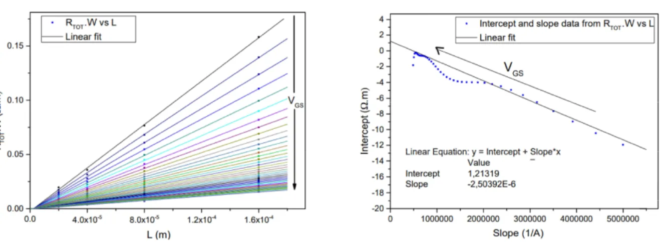
Figure 2.1:Rtot vsLplot
for contact resistance ex-traction method
As the total resistance (Rtot) is equal to the sum of the channel
resistance (Rch) and the parasitic resistances, mainly the contact
resis-tance (RDS), we can use equation 1.4a to write[18]:
RtotW = 1
K(VGS−VT)α−1
(L+∆L) +RDSW (2.1)
By plotting RtotW in function of L, and fitting linearly the points
with the sameVGS, a graphic similar to Figure 2.1 would be obtained.
C H A P T E R 2 . M E T H O D O L O G Y
Ideally, all the lines correspondent to differentVGS values would tend to the same point when
approaching the limit of a zero-length resistor. The intercept of the lines with the y-axis would then be equal toRDSW. But the parameter variation in the devices causes a shift on the position
of the intercepts:
• The effective channel length of the device may have a bias dependence causing the
inter-cept points to depend onVGS[27]
• The intercepts may also not occur all in the same point due to errors in the fabrication process that cause the actual channel length of the device to be different from the mask.
So in order to obtain the contact resistance, the slope(m) and intercept(B) values of theRtotW
vsLdata are extracted using linear fitting. Then B vs m is plotted, where:
m= 1
K(VGS−VT)α−1
(2.2)
B= ( 1
K(VGS−VT)α−1)∆L+RDSW (2.3)
The value of the contact resistance can be extracted from this plot, as the y-axis intercept corresponds toRDSW.
The method has the disadvantage of not providing separate information about the drain and the source contact resistances [28] and assuming the contact resistance is not modulated by any bias. To observe if the contact resistance may exhibit some dependence on the applied gate voltage another method of extraction may be used. To determine the contact resistance and∆L
at a certainVGS, two separate voltagesVGS-∆VGS andVGS+∆VGS are used (where∆VGS is an
arbitrarily small voltage).[29] The previous used method of the transmission line measurement is then applied for each pair of values, obtaining a solution of contact resistance and∆L that
provides a close approximation for the values at a certainVGS. [29]
2.1.1.3 Power parameter
The power parameter (α) can be extracted from the (IDS−VDS) characteristics of the devices.
Considering the transconductance expressed asgm= ∂IDS
∂VGS, the expression can be obtained from
equation 1.4a [18] :
IDSlin
gmlin =
VGS−VT −VDS 2
α−1
VDS
VDS−RDSIDSlin (2.4) By plotting IDSlin
gmlin in function ofVGS, we are able to extractαfrom the slope.
2.1.1.4 Transconductance parameter
The extraction of the transconductance parameter (K) is based on the slope of theRtotW vsLdata.
The slope m (equation 2.2) raised to−α1−1 is plotted in function ofVGS-VT. The slope of the fit is then equivalent to K raised to α1−1. [18] The mobility value can be obtained from K.
2 . 1 . PA R A M E T E R E X T R AC T I O N M E T H O D S
2.1.1.5 Channel length modulation parameter
The channel length modulation parameter (λ) can be obtained by dividing the Lef f for the
equivalent of the Early Voltage for the TFT (also named VA). VA is the absolute value of the intercept of the output characteristics on theVDSaxis.[18]
It is incorporated in the model equations by the parameter xcm(equation 2.5):
xcm= 1 +
λVDS Lef f
(2.5)
In this equationLef f is the sum of the channel length (L) with the channel length change (gate
bias dependent∆L).
2.1.1.6 Saturation parameter
The saturation parameter (αsat) relates the applied gate bias of the transistor with the saturation
voltageVDSsat, the drain voltage at which the transistor enters the saturation region. It can be
rewritten as the saturation current parameter (γsat) by the equation[18]:
γsat= 1−(1−αsat)α (2.6)
γsat can be extracted from the saturation region measurement data. The slope (S) of the fit of (IDSLWef f) to the power of α1 plotted in function ofVGS yields[18]:
γsat= αS α
xcmK (2.7)
2.1.2 Transconductance extraction
The transconductance (gm) is extracted from the partial derivative of IDS with respect toVGS
(∂IDS
∂VGS). It is used in the small-signal model to relate the drain current toVGS.
2.1.3 Capacitance-Voltage Measurement
The extraction of the Capacitance-Voltage (C-V) characteristics was performed using Keysight B1500A and a Cascade EPS150 Triax probe station for the device with a normal gate to source/drain (S/D) C–V configuration, at small signal voltage of 30 mV and frequency f = 10 kHz. The 2-terminal voltage sweep was performed with applied gate voltages from -5 to 10 V, and drain voltage of 0 V with the source open and small signal frequency f = 10 kHz.
2.1.3.1 Dielectric and overlap capacitance
The overlap capacitance (Cov) is composed of the drain overlap capacitance (Covd) and the
source overlap capacitance (Covd). Assuming the symmetry of the device, Covdand Covsare both
the same value and equal to 12Cov. We are able to extract the values of these capacitances from the CV curves measured from the device (Figure 2.2 exhibits an example of a CV curve from a TFT). At lowVGS the device is in the depletion zone, which causes the channel capacitance to
become zero. [30]The gate capacitance is saturated atCMIN, due to the parasitic capacitances of the transistor.
C H A P T E R 2 . M E T H O D O L O G Y
Figure 2.2: Gate-source
ca-pacitance example
We can assume CMIN =Cov as the overlap capacitance is the
largest of the parasitic capacitances. For higher values of VGS
the channel capacitance starts to increase, until saturation occurs atCMAX due to the more dominant response from free carriers provenient from the conduction band.[30]Cican be extracted from
CMAX (equation2.8):
Ci=(CMAXW L−CMIN) (2.8)
2.1.4 AC Measurement
A Keysight E5061B network analyser with model 10 high frequency probes (6 GHz bandwith) calibrated by a GGB Industries, Inc. CS-11 calibration substrate was used to measure the parameters. The network analyser provided the DC bias from port 1 (connected to the gate of the transistor) whereas the DC bias from port 2 (supplying the transistor drain) was provided through an Agilent 33500B series waveform generator. The network analyser separates the AC small signal input and output from the DC component provided from port 1, but the same does not happen for the DC bias originating from the generator. In order to avoid interfering with the analyser circuitry, a Picosecond 5546 bias tee is used.
The gate was biased at 8 V and the drain at 10 V in order for the TFT to be in saturation. The device chosen for the S parameter analysis had the largest W/L ratio (channel width of 160 µm and a channel length of 20µm) in order to avoid machine errors related to the minimum current level detected by the apparatus. To further reduce the noise, due to the very small signal, the noise obtained when lifting the probes was removed from the data.
Note: All the measurements were performed both in UCAM and in CENIMAT in different
stages of the project.
3
Analysis of Results
3.1 DC Model
The linear equation parameters were extracted from the transfer curves (VDS=5 mV and aVGS sweep from 0 to 15 V) of four devices with channel width of 20µm and channel lengths of 20, 40, 80 and 160µm. TheIGS value was also measured in order to analyse the gate leakage. The
saturation parameters were extracted from the output characteristic curves (VGS values varying from 6 to 10 V with a 1 V step and aVDSsweep from 0 to 16 V) and the transfer curves (VDS=10
V and aVGS sweep from 0 to 10 V).
3.1.1 Threshold voltage
The second derivative method is highly sensitive to noise, so the use of smoothing functions was necessary in order to obtain a readable result. However, samples have a slow transition from subthreshold to linear phase and using the second derivative method (refered in subchapter 2.1.1.1) still provided results difficult to interpret. The nonlinear behavior around the threshold
voltage creates a smooth curve instead of an abrupt peak as we are able to observe in Figure 3.1a. By examining the graphic we are able to estimate the threshold voltage to be around 4 V, but not the exact value. This lead to the choice of linear fitting as the method used forVT
extraction in the first model.
At a relatively lowVGnear the threshold voltage, the behaviour is still nonlinear, so those
values were excluded. The same occured for very high values ofVGS, where the current (and possibly charge accumulation in the channel) does not increases linearly withVG even at the
very low appliedVDS. The fitting was performed for the interval of 6 to 12 V (Figure 3.1b), as
the value forVT had been roughly estimated to be 4 V. The same procedure was repeated for the remaining transistors, and the results were similar for all the dimensions (table 3.2 exhibits the extractedVT values).
(a) Plot of Second derivative of IDS vs VGS for
TEStransistor with 20/160 ratio
(b)Plot ofIDSvsVGSwith appliedVDS=5 mV and
TESlinear fitting for transistor with 20/160 ratio
Figure 3.1:Methods of threshold voltage extraction
C H A P T E R 3 . A N A LYS I S O F R E S U LT S
3.1.2 Contact resistance
(a) Plot and linear fitting of Rtot.W vs L data
TESfor various values ofVGS-VT (from 1 to 10 V
TESwith 0.1 V intervals)
(b)Linear fitting of Intercept vs Slope data from
TESRtot.W vs L
Figure 3.2:Contact resistance extraction
The contact resistance was extracted from the transfer curves of transistors with four dif-ferent channel lengths at low appliedVDS (5 mV). The Rtot values were obtained by dividing
the appliedVDS by the drain current measurements. Following the contact resistance TLM
extraction procedure (described in section 2.1.1.2) results in various values of intersections (Figure 3.2a).
In order to obtain a RDS value the slope (m) and intercept (B) values of the fitted RtotW vs L data were plotted (Figure 3.2b). The RDSW value obtained was of approximately 1.2Ωm which
is equivalent of a contact resistance of 60 000Ωfor a transistor with a channel width of 20µm.
From this data we are also able to extract the effective channel length.The average L value for
all the intersections of Rtot.W vs L linear fit was -1µm, which is the value for∆L according to
equation 2.1.
3.1.3 Power parameter
The power parameter was extracted for values ofVGS higher than the threshold voltage (VGS
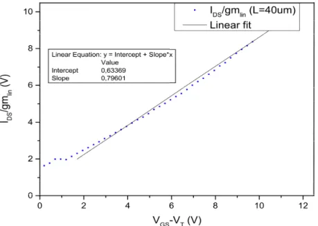
-VT>1) to minimize the contact resistance error. The method described in section 2.1.1.3 was performed (Figure 3.3), using the data from a transistor with dimensions W=20µm and L=40 µm. The values of IDSlin
gmlin for appliedVDS of 5 mV were plotted in function ofVGS-VT, and the
slope obtained through a linear fitting.
The value ofαused in the model was 2.26, as the slope value was approximately 0.796.
3.1.4 Transconductance parameter
The slope values of the Rtot.W vs L data (obtained previously when extracting the contact
resistance) were raised to 1.126 and then plotted in function ofVGS-VT (Figure 3.4).
The fitted line had a slope of approximately 2.75×10⁻⁶and intercept of 1.2×10⁻⁷. The obtained K value was of 1×10⁻⁷FV−1s−1cm−1as the value ofαis 2.26.
3 . 1 . D C M O D E L
Figure 3.3:Linear fitting ofIDS/gmlin versusVGS-VT for a transistor with dimensions W=20µm and
L=40µm
Figure 3.4:Linear fitting of m to the power of−α1−1 in function ofVGS-VT
3.1.5 Channel length modulation parameter
VA extraction was performed forVDS values above 13 V. In this way the fitting was always performed on the saturation region, regardless of the applied value ofVGS (varied between 5
and 15 V).
The average of the obtained |VA| values (table 3.1) was calculated (excluding the more
dissimilar values), resulting in the value of 1842 V, which yielded aλvalue of 1.09×10⁻⁸m/V.
C H A P T E R 3 . A N A LYS I S O F R E S U LT S
Figure 3.5:Linear fitting of saturation region for the output curves of a transistor with dimensions W
and L equal to 20µm
Table 3.1:ObtainedVAvalues for all the appliedVGScurves
VGS(V) 5 6 7 8 9 10 11 12 13 14 15
|VA|(V) 802 1458 13804 4954 13759 5022 2215 1044 528 347 215
3.1.6 Saturation parameter
The transistor with the longest channel length (L=160µm) was used in order to reduce contact resistance effects. The plot of (IDSLef f
W ) to the power of 1α in function ofVGS was linearly fitted
(Figure 3.6) and the slope value extracted. Theγsat value obtained was of 0.63, as the slope
value was approximately S=4.6×10⁻⁴Aα1.
3.1.7 Model fitting
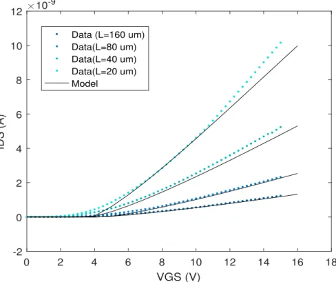
The parameters used for the linear fitting are summarized in table 3.2, and were used in equa-tion 1.4a in order to obtain the model linear transfer curve (Figure 3.7).The γsat value was
slightly altered to improve the continuity of the model.
The equation 1.4a was used for the transfer curve linear fitting. For the output curves fitting, equations 1.4a and 1.4b were altered and a transition function was added in order to obtain a better modeling of the transition region (equations 3.1a and 3.1b).
3 . 1 . D C M O D E L
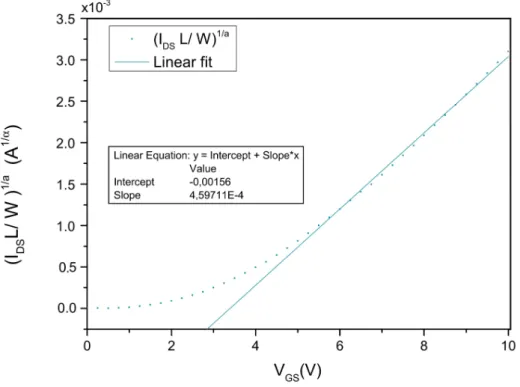
Figure 3.6:Linear fitting of (IDSlinWL)
1
α in function ofVGS for a transistor with dimensions W=20µm ans L=160µm
Table 3.2:Extracted parameters summary.
Transistor Length VT Contact Resistance ∆L α K λ γsat
(µm) (V) (Ω) (µm) (F/V.s) (µm/V)
20 3.8
40 3.8 60 000 1 2.26 1×10⁻⁷ 0.01 1.023
80 4.5
160 4.3
IDS=
KW
L (VGS−VT− VDS
2 )α−1(VDS−IDSRDS−(1−
1
α)(VDSint−IDSRDS)
α Lin.(3.1a)
K α
W
L γsat[(VGS−IDS RDS
2 −VT)αxcm Sat.(3.1b)
WhereVDSint=(VDS−m+ (VGS−VT)−m))−1m. The parameter m is an adjustment parameter related
to the sharpness of the knee region. The plotted model is depicted in Figures 3.7 and 3.8.
The fit is best in the region from which the threshold voltage was extracted (approximately 6 to 12 V). Above a certain value ofVGS we observe an increase on the measured drain current and transconductance, which are not reproduced by the model.
Possible reasons for the obtained fitting were mentioned in section 2.1.1.2, and relate to the method of contact resistance extraction. The mobility extraction could also be a possible source
C H A P T E R 3 . A N A LYS I S O F R E S U LT S
0 2 4 6 8 10 12 14 16 18
VGS (V) -2 0 2 4 6 8 10 12 IDS (A)
#10-9
Data (L=160 um) Data(L=80 um) Data(L=40 um) Data(L=20 um) Model
Figure 3.7:Linear fitting of model with VGS dependent contact resistance and∆L for applied VDS of 5
mV
of error, as the effective mobility is a difficult value to extract, depending on the values of other
extracted parameters such asVT. The output curves forVGS values from 8 to 12 V are depicted in Figure 3.8. The modelled output curves fail to simulate the transistor behaviour, fitting only for the values of 9 and 10 V.
3.1.8 Bias dependent parameters
In order to improve the poor model fit several measures were taken, such as investigating the possibility of channel length fabrication errors, and bias dependence of the parameters that was not taken into account. The threshold voltage was extracted from the transfer curves (VDS=100 mV and aVGS sweep from 0 to 18 V) of three devices with channel width of 20µm and channel
lengths of 40, 80 and 160µm. TheVDSwas slightly increased but the device was still operating
in the linear region. The objective was to increase the current value and reduce the noise that could affect the extraction of parameters. The device with channel length of 20µm was excluded
so as to minimize contact resistance effects.
The samples were analysed using an optical microscope, where the channel length was measured and compared with the mask channel length. It was concluded that the physical length did not differ significantly from the mask dimensions (C). The effective channel length
was then tested, as it can suffer from a bias dependency [31] which could be significant enough
to influence the fit. A different extraction method for the contact resistance and effective channel
length (referred in chapter 2.1.1.2) was used. The extraction procedure is quite similar to the one previously performed, except applied to a pair of values varying 0.03 V (the value of∆VGS)
from theVGS the contact resistance solution is being extracted.
3 . 1 . D C M O D E L
0 2 4 6 8 10 12 14 16
VDS (V)
0 0.5 1 1.5 2 2.5 3 3.5
IDS (A)
#10-6
Model Data
Figure 3.8:Linear fitting of model withVGSdependent contact resistance and∆L for appliedVDSof 10
V
From it the results from table 3.3 were obtained.
Table 3.3:Extracted parameters summary.
VGS-VT (V) Contact Resistance . W (Ω.m) ∆L(µm)
1 2.80 -0.56
2 1.21 -1.26
3 1.26 -1.22
4 1.21 -1.27
5 0.84 -1.68
6 0.66 -1.92
7 0.35 -2.42
Average value 1.19 -1.47
The extracted contact resistance exhibits bias dependency as the value appear to decrease with increasing gate bias. The same is verified for the extracted∆L values, which decrease with
appliedVGS meaning that the effective length decreases with gate bias.
The average value (1.19Ω.m) means that for these transistors of 20µm width the contact
resistance would be 59 500Ω, very similar to the value extracted for the first model fit (of 60
C H A P T E R 3 . A N A LYS I S O F R E S U LT S
000Ω). But if the contact resistance bias theory is correct, it varies from 17 500Ωto values
higher than 100 000Ω. This may be the explanation for some discrepancies on the the first
model fitting.
Table 3.4:Extracted parameters summary.
Transistor Length (µm) Vt (V) Alpha K (F/V.s) λ(µm/V) γsat
40 5
80 6 2.55 4.5×10⁻⁸ 8.89×10⁻⁸ 1.19
160 6
The remaining parameters were extracted by the same methods previously used (in sub-chapters 3.1.3, 3.1.4, 3.1.5 and 3.1.6). Table 3.4 exhibits the extracted values for the parameters.
3.1.9 Second Model fitting
0 2 4 6 8 10 12 14 16 18
VGS (V) -2 0 2 4 6 8 10 12 14 IDS (A)
#10-8
Model
Data (L=40um) Data (L=80um) Data (L=160um)
Figure 3.9:Linear fitting of model withVGSdependent contact resistance and∆L for appliedVDS of 100
mV
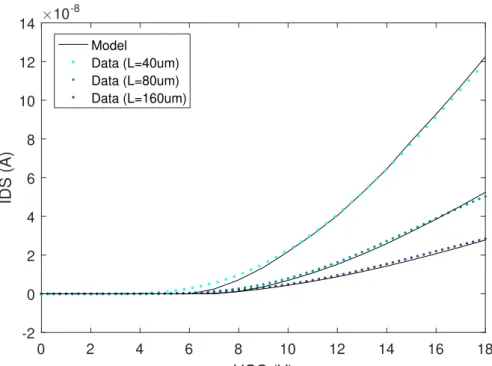
Using the variable contact resistance values it was possible to improve the fitting of the model. The model fit the measured transfer curve of the transistor even at higher values of VGS, behaving better than the first model. The region near the threshold was not as effectively
modelled, however the transistor does not behave as linearly in that region so the worse fit was expected. The model did not achieve a reasonable result for the saturation region (Figure 3.10). The effective mobility value could be the responsible for the fit, as the extraction method
depends on the values of VT and is sensitive to contact resistance, and therefore disposed to
errors. We observe that the scaling of model curves is higher than the data, and there is an
3 . 1 . D C M O D E L
0 2 4 6 8 10 12 14 16
VDS (V) 0 2 4 6 8 10 12 14 16 18 20 IDS (A)
#10-8
Data Model
Figure 3.10:Linear fitting of model withVGSdependent contact resistance and∆L for appliedVDS of
100 mV
overestimation of the drain current. A better fitting can be obtained when scaling the model by
1
2 (Figure 3.11). This could indicate errors with the power and transconductance parameters,
which are related to the transistor’s mobility.
0 2 4 6 8 10 12 14 16
VDS (V) 0 2 4 6 8 10 12 14 16 18 20 IDS (A)
#10-8
Data Model
Figure 3.11:Linear fitting of lower mobility model withVGS dependent contact resistance and∆L for
appliedVDS of 100 mV
In order to analyse the fitting of the output curve, the saturation mobility was calculated,
C H A P T E R 3 . A N A LYS I S O F R E S U LT S
using the formula expressed in equation 3.2[32].
µsat=
∂√ID
∂VGS 2
1 2CiWL
(3.2)
The objective was to compare the value of the effective mobility to the saturation mobility
and see if the difference was very significant, indicating that the effective mobility could have
extraction errors. The transfer curve for the transistor with W=20µm and L=80µm with an applied VDS of 10 V was used, obtaining the plot depicted in Figure 3.12. We are able to
Figure 3.12:Plot of saturation mobility versusVGSfor a transistor with W=20µm and L=80µm with an
appliedVDS of 10 V
observe that the mobility value increases with appliedVGS until approximately 10 V, but for
higherVGS values the mobility starts to decrease. The highest mobility value is 3.7 cm2V−1s−1,
that results in a K of approximately 1.4×10⁻⁷ F/V.s. This value is higher than the extracted
beforehand, so there is a significant difference in the values of mobility in the model and data,
which influences the values of the parameters that depend on that extraction. Therefore another method for the extraction of the effective mobility should be used on these devices.
3.2 AC Model
3.2.1 Transconductance
In order to obtain the device transconductance for the small signal model, the first derivative of the drain current in function ofVGS was plotted (Figure 3.13). This value is normally constant in the saturation region as the change in drain current is not as noticeable, however that was not the case for the obtained values as it continued to increase. The gm value for the bias point conditions (VDS=10 V andVGS=8 V) is of approximately 4×10⁻⁶ 1
Ω.
3 . 2 . AC M O D E L
Figure 3.13:IDS and first derivative ofIDSin function ofVGSwith appliedVDS of 10 V for gm extraction
3.2.2 Dielectric and overlap capacitance
The values of capacitance in function of gate-source voltage were extracted for the transistor with dimensions W=160µm and L=20µm(Figure 3.14). The measurements were repeated and the average of the values obtained. The value of CMIN obtained was of 6×10⁻¹³F which can
be divided in order to obtain the source and drain overlap capacitances. The average value of CMAXwas 1.9×10⁻¹²F so the Cch (gate capacitance) value calculated to be of 1.3×10⁻¹²F.
Figure 3.14:Capacitance measurement for transistor with dimension 160/20µm
The summary of extracted capacities and transconductance of the device can be found on table 3.5. As the gate capacitance value is known, we are able to obtain the gate capacitance per
C H A P T E R 3 . A N A LYS I S O F R E S U LT S
unit of areaCi, which is 40.62 nF/cm2.
Table 3.5:High frequency parameters summary.
Gate capacitance (F) Overlap capacitance (F) g0(1/Ω) gm(1/Ω)
1.3×10⁻¹² 3×10⁻¹³ 1/50 4×10⁻⁶
3.2.3 S parameters fitting
The S parameters were measured from a frequency of 1 kHz to 1 GHz. The TFT was biased at VG=8 V andVD=10 V in order to be in the saturation region and obtain a good performance. The fitting for the S11, S21, S22parameters was performed with the equations obtained from the
small signal model (Appendix A) and the h21with equation 1.6.
3.2.3.1 S11
103 104 105 106 107
Frequency (Hz)
-0.5 -0.4 -0.3 -0.2 -0.1 0 0.1 0.2 0.3 0.4 0.5
Magnitude (dB)
Magnitude of S11 Parameter
Model Data
Figure 3.15:Fitting of S11magnitude
The S11was the parameter that was most affected by low frequency noise. As the value is
very close to 0 dB, any oscillations may influence greatly its value and the value of the obtained current gain. The fitting of the S11magnitude is good until the frequency of 50 MHz, where
the data starts to exhibit a drop and the model stays constant. This difference is exarcerbated
with the increase of the frequency as the model only starts to drop at frequencies above 100 MHz. However, as the cutofffrequency of the device is lower than 50 MHz (fT is 1 MHz as it
will be discussed later in section 3.2.4), the fitting for the operating frequencies is acceptable, with the model having a very small relative mean square error of 0.12 for the total measured frequency range, and 15µfor the working frequencies under fT. The relative mean square error
3 . 2 . AC M O D E L
was calculated from equation 3.3:
rMSE=1 n
n
X
t=1
( ˆYi−Yi)2 (3.3)
Where n is the number of data points, ˆYi the prediction values vector and Yi the measured
values vector.
103 104 105 106 107
-5 -4 -3 -2 -1 0 1 2 3 4 5 Phase (deg) Model Data Bode Diagram
Frequency (Hz)
Figure 3.16:Fitting of S11phase
The same is observed for the S11phase (Figure 3.16, with the model not fitting as well for
higher frequencies above the cutoffwhere the data exhibits a drop.
105 106 107 108 109
Frequency (Hz) -0.6 -0.4 -0.2 0 0.2 0.4 Magnitude (dB)
Fitting of S11 Parameter data
Fitting Data
(a)Fitting of S11magnitude with function
103 104 105 106 107 Frequency (Hz) -0.6 -0.4 -0.2 0 0.2 0.4 0.6 Phase (deg)
Fitting of S11 Parameter data
Data Fitting
(b)Fitting of S11phase with function
Figure 3.17:Fitting of S11data with function
Some discontinuities exist in the S11parameter data, that can cause errors when obtaining
the device’s current gain. This occurred when removing the measurement noise due to the very
C H A P T E R 3 . A N A LYS I S O F R E S U LT S
low value of the parameter. As the model being used is the MOSFET, the presumption of there being only one influential pole at low frequencies in the S11parameter is valid. Taking that
assumption into account, in order to reduce the noise caused by the measurement a function was used to fit the extracted data:
H(s) = A
Bs+ 1 (3.4)
The obtained values for the constants were A=1 and B=6×10⁻¹⁰, which signifies that the pole
would be located at approximately 2.7×10⁷Hz.
It is possible to observe in figures 3.17a and 3.17b that although the fitting does remove the discontinuities that could have caused errors in the calculation of the current gain, it does not completely translate the S11 parameter. There is a slight magnitude drop that occurs on the
data and not on the fitting. The cause may lay in the assumption that only one pole is present at lower frequencies, and indicates that the MOSFET model is too simplistic to explain the TFT high frequency behaviour.
3.2.3.2 S21
103 104 105 106 107
Frequency (Hz) -90 -85 -80 -75 -70 -65 -60 -55 -50 Magnitude (dB)
Magnitude of S21 Parameter
Model Data
Figure 3.18:Fitting of S21magnitude
The S21model only fits the data for frequencies above 10 kHz. For lower frequencies the
MOSFET model tends to the value−2ggm0 (obtained from equation A.5 when s tends to zero). The value of gmcan be assumed correct, as the model and the data coincide at lower frequencies between 10 kHz and 1 MHz. However the measured data magnitude at low frequencies is not constant, but increases with the frequency until a constant value is met at approximately 10 kHz, meaning that at least an extra zero and pole exist at lower frequencies that were not described in the model.
For frequencies above 1 MHz the fitting error increases with the frequency. This is observed in Figure 3.19 as the data phase suffers from noise at higher frequencies.The error for the S21
3 . 2 . AC M O D E L
103 104 105 106 107
45 90 135 180
Phase (deg)
Model Data
Bode Diagram
Frequency (Hz)
Figure 3.19:Fitting of S21phase
fitting is of 9.9, a higher value than S11that indicates the fitting deviates from the data. If only
considering the frequencies lower than fT the error is even higher, of 17.8.
3.2.3.3 S22
103 104 105 106 107
Frequency (Hz)
-0.04 -0.03 -0.02 -0.01 0 0.01 0.02 0.03 0.04
Magnitude (dB)
Magnitude of S22 Parameter
Model Data
Figure 3.20:Fitting of S22magnitude
The S22parameter is zero dB at low frequencies, exhibiting only some noise variations that
slightly alter this value. as the value is so reduced, the measured data noise causes a higher error than the other fittings, of 24.8. If the measuring noise is ignored, the model appears to describes well the TFT for all the operating frequencies and until the frequency of 20 MHz.
C H A P T E R 3 . A N A LYS I S O F R E S U LT S
Above that value, the data starts to exhibit some degradation that is not observed in the model.
103 104 105 106 107
-0.5 -0.4 -0.3 -0.2 -0.1 0 0.1 0.2 0.3 0.4 0.5 Phase (deg) Model Data Bode Diagram
Frequency (Hz)
Figure 3.21:Fitting of S22phase
The same is observed for the S22parameter phase, as only above a high frequency (higher
than the cutofffrequency) we observe a significant deviation from the measurements.
3.2.4 Current Gain
The h21equation was obtained from the small signal model (equation 1.6) and the extracted
parameters applied. The intrinsic current gain was derived from the measured S parameters, using the equation A.8 (presented in appendix 1), and plotted with the model expression (Figure 3.22). We can observe that for frequencies above 10 kHz the current gain decays with increasing frequency as it is expected for a field effect transistor, following the 1
f (-20 dB/decade) slope.
There is a discrepancy between the model and data, as the model exhibits the same behaviour at a slightly lower magnitude value for frequencies above 10 kHz. Between 1 kHz and 10 kHz there is a notable difference: the model displays the same slope value and the slope of the data
varies. We can presume the cause to be the existence of an extra pole that is not described on the model at the measured frequencies. The parasitic resistances and their connections vary and affect the device in a significant way, creating poles and zeros that are most likely the reason
why the MOSFET model could not adapt to the TFT.
The fT for the TFT was found to be about 1 MHz, differing from the model which predicted
the lower value of 0.7 MHz. We can analyse the current gain in order to understand what which S parameter had more influence the fitting. We are able to rewrite equation A.8 as [22]:
h21=
S21
(S11−1)(S22+ 1)
(3.5)
The termS21S12is small as most of the power is reflected and not transmitted. According to the
experiments the (1−S11)(1 +S22) term is significantly larger, and dominates overS21S12(Figure
3 . 2 . AC M O D E L
103 104 105 106 107 108 109
Frequency (Hz) -20 -10 0 10 20 30 40 50 60 Magnitude (dB)
Modeling of H21 Parameter
Data Model
Figure 3.22:Fitting of h21
3.23a) . The denominator can be approximated to be (1−S11)(1 +S22), as the approximation
coincides with the parameter (Figure 3.23b).
103 104 105 106 107 108 109
Frequency (Hz) -250 -200 -150 -100 -50 0 Magnitude (dB)
S Parameter term comparison
(S12S21 ) (1-S11 )(1+S22 )
(a)Plot ofS21S12and (1−S11)(1 +S22)
103 104 105 106 107 108 109
Frequency (Hz) -20 -10 0 10 20 30 40 50 Magnitude (dB) h21 comparison h21
S21/((1-S11)(1+S22))
(b)Comparison of h21parameter with approximation
Figure 3.23:h21approximation comparisons
As the error from parameterS11 is small, the h21 fitting error is caused mainly due to
parameterS21andS22. This raises the question of the fitting error being partially caused due
to machine noise which could alter significantly the low value of S22. The errors caused by
S21however are visibly due to lacking components in the traditional MOSFET model, whose
connections create zeros and poles not described in the model’s equations when applied to a TFT.