An alternative method to determine oxygen concentration in industrial monocrystalline silicon has been developed and tested, resorting to statistical analysis and modeling. The model has been applied to different set samples, with a prediction accuracy varying between 90% and 95%. This model works on the assumption of a very effective heat treatment for thermal donor killing and similar thermal history of the produced/analyzed ingots.
João Martins v
Table of Contents
Abstract ... iii
List of Figures ... vii
List of Tables ... ix
Acknowledgments ... xi
List of Abbreviations and Symbols ... xiii
Chapter 1 - Introduction ... 1
1.1. Motivation ... 1
1.2 PV industry and Norway ... 1
Chapter 2 - Semiconductors ... 3
Chapter 3 - Silicon crystal ... 5
Chapter 4 - Czochralski crystal growth ... 9
4.1. CZ Puller ... 9
4.2. CZ crystal growth procedure ... 10
Chapter 5 - Impurities ... 13
5.1. Dopants ... 14
5.2 Oxygen ... 14
5.3. Thermal Donors ... 15
5.4. Carbon ... 17
Chapter 6 - Sample preparation ... 19
Chapter 7 - Characterization techniques and methods ... 21
7.1. Four Point Probe ... 21
7.2. FTIR ... 22
7.3. Measurement Procedure ... 24
7.4. Measurement Errors ... 24
Chapter 8 - Modeling ... 27
8.1. Curve fitting ... 28
8.2. Least Squares and average error ... 29
8.3. Models ... 31
Chapter 9 - Results ... 33
9.1. Radial oxygen variation ... 33
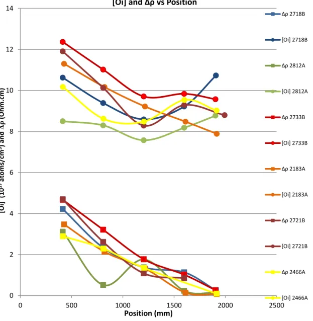
9.2. Oxygen and Resistivity Axial Variation ... 34
9.3. Oxygen concentration BHT and AHT... 35
9.4. Oxygen and Resistivity Variation for fixed position ... 36
vi João Martins
9.6. TX Model Results ... 40
9.7. TX model results: Filtered sample set ... 44
9.8. Model Results: [Oi] BHT vs [Oi] AHT ... 46
9.9. Heat treatment performance analysis ... 48
9.10. Simulation Results ... 48
Chapter 10 - Discussion/Analysis ... 49
Chapter 11 - Conclusion ... 53
Chapter 12 - Further Work ... 55
Chapter 13- References ... 57
João Martins vii
List of Figures
Figure 1: Norwegian public R&D budgets for solar energy during the last decades (million €). Source: [2]. Note the exponential growth in investment in PV R&D during the end of the previous decade. ... 2 Figure 2: Energy band diagrams for general electric insulators, semiconductors and metals. Source:[6]. Eg stands for energy gap, which is the energy that an electron must gain to leave the conduction band and pass to the valence band through the band gap. Metals have no band gap, so any electron can freely travel between both bands. Insulators, on the other hand, have too large of a band gap to allow electrons to travel from one band to another. Finally, semiconductors have the propriety of having a band gap sufficiently small to allow electrons within a certain energy level to move to the valence band. ... 4 Figure 3: Siemens reactor schematic for poly-Si production. Source: [9]. Gaseous molecules containing silicon elements in their constitution are injected in a quartz closed structure. The silicon will be separated from the gas by contacting very hot silicon rods and form crystallites along the rod, resulting in grown multi crystalline ingots. ... 6 Figure 4: Poly-Si solar cell (left) and mono-Si solar cell (right) [10]. Note the clear crystal formations in the poly-Si solar cell versus the homogeneous visual appearance of mono-Si solar cell. ... 6 Figure 5 (Source: [11]); 6 (Source: [12]): schematic of FZ technique (left) and picture of the molten region during FZ process (right). At inert argon atmosphere, a polycrystalline silicon rod is placed inside the device. Induction coils heat silicon axially in a small length range. Those coils move along the ingot, allowing impurities to segregate to one end of the ingot, resulting in extremely pure crystals. oxygen concentration in FZ-Si is extremely low, since it does not resort on a crucible to contain the silicon melt, which is the main oxygen source of CZ-Si. ... 7 Figure 7: Schematic of CZ puller. Source: [20]. Notice the hot zone surrounding the crucible, the crystal and crucible rotation mechanisms and inner chamber gas flows. ... 10 Figure 8: Schematic of CZ crystal growth [21]. Firstly, the melt of the feedstock occurs. After temperature stabilization, the crystal seed is lowered and the necking starts. After the body of the crystal is fully grown, the ingot is slowly detached, forming the tail. ... 11 Figure 9: Power dependency n of TD formation (circles) and loss of Oi atoms (crosses) versus annealing temperature. Source: [31]. ... 16 Figure 10: Four Point Probe Schematic [39]. Due to the distance between each probe and due to different pairs of probes being used respectively for current appliance and voltage measuring, contact resistance is eliminated, leading to very accurate measures, even for thin samples with low resistance. ... 22 Figure 11: FTIR Spectrometer Schematic [54]. The moving mirror, at the top right corner, allows for a certain range of frequency measures, with a very high resolution. Since the optical path includes a segment that forces the beam to transverse the sample, which is in the room atmosphere, it is important to resort to frequent air purging and background checks, for precise measures. ... 23 Figures 12; 13; 14: Oxygen concentration (center and borders) versus Position. Blue lines stand for oxygen measured in the center, red lines stand for the average oxygen measured near the borders of the wafers. ... 33 Figure 15: Oxygen and resistivity variation VS position. Each color represents a specific ingot, circles represent oxygen concentration and squares represent resistivity variation ... 34 Figures 16; 17; 18; 19; 20; 21: oxygen concentration BHT and AHT versus position. Red lines stand for oxygen AHT and blue lines stand for oxygen BHT. ... 35
viii João Martins Figures 22; 23; 24; 25; 26: oxygen concentration versus variation of resistivity. The amplitude
values for the positions ranges T1, T2, T3 and T4 are 40mm. T5 presents an amplitude value of 122 mm... 37 Figure 27: Base model results for oxygen concentration predictions along the ingot. Note the clear position groups. ... 38 Figure 28: Base model results for oxygen concentration predictions, in function of variation of resistivity. ... 38 Figures 29, 30, 31, 32, 33, 34: Examples of the base model application in specific ingots. The first pair of examples show an average correlation, the second pair a good correlation and the third pair a bad correlation. Blue lines represent measured values and red lines represent estimated values. ... 39 Figure 35: TX model results for oxygen concentration predictions along the ingot. ... 40 Figure 36: TX model results for oxygen concentration predictions, in function of variation of resistivity. ... 40 Figure 37: TX model results for oxygen concentration predictions, in function of variation of resistivity, first position group ... 41 Figure 38: TX model results for oxygen concentration predictions, in function of variation of resistivity, second position group. ... 41 Figure 39: TX model results for oxygen concentration predictions, in function of variation of resistivity, third position group. ... 41 Figure 40: TX model results for oxygen concentration predictions, in function of variation of resistivity, forth position group. ... 42 Figure 41: TX model results for oxygen concentration predictions, in function of variation of resistivity, fifth position group. ... 42 Figures 42, 43, 44, 45, 46, 47: Examples of the TX model application in specific ingots. The first pair of examples show an average correlation, the second pair a good correlation and the third pair a bad correlation. Blue lines represent measured values and red lines represent estimated values. ... 43 Figure 48: Base model results for oxygen concentration predictions along the ingot, applied for partial batch. ... 44 Figure 49: Base model results for oxygen concentration predictions, in function of variation of resistivity, applied for partial batch ... 44 Figures 50, 51, 52, 53, 54, 55: Examples of the TX model application in specific ingots, for a partial batch. The first pair of examples show an average correlation, the second pair a good correlation and the third pair a bad correlation. Blue lines represent measured values and red lines represent estimated values. ... 45 Figure 56, 57, 58, 59, 60, 61, 62, 63, 64, 65, 66, 67: Ingots characterized to compare model results using either before heat treatment (BHT) or after heat treatment (AHT) oxygen concentration measures. Red lines represent predicted values and blue lines represent measured values... 47 Figure 68: Cooling curve drawn from the simulation results. ... 48 Figure 69: Base model results. Red lines represent estimated values and blue lines measured values... 65 Figure 70: TX model results. Red lines represent estimated values and blue lines measured values... 67 Figure 71: TX model results (partial batch). Red lines represent estimated values and blue lines measured values. ... 68
João Martins ix
List of Tables
Table 1: Heat treatment performance analysis results. T1 are the samples close to the seed and T5 are the samples close to the tail. ... 48 Table 2: Crystal growth simulation results... 48 Table 3: Minimum, maximum and amplitude values for the complete data set. ... 61 Table 4: Data acquired to compare heat treatment performances. AP stands for After Polishing. ... 62 Table 5: Samples’ main data. ... 73
João Martins xi
Acknowledgments
For any master’s student, the thesis is most likely the most important project one has during their academic course. As for me, the opportunity that was given to me to work, both in a historical university such as NTNU and in a successful company such as NorSun was priceless. I never thought I’d have such a chance, nor did I think that it would be such a positive experience, not only professionally, but also for personal development.
Firstly, I would like to give my dearest regards to Professor Marisa Di Sabatino, my supervisor at NTNU, for her invaluable guidance through what was a whole new world for me.
I want to mention the role of Professor João Serra, my supervisor at FCUL, since I would not have had this chance without him, as well as for his useful advice during this project.
My deepest gratitude goes to Yu Hu, my co-supervisor and friend, who guided me through my time in NorSun. Even through a strict schedule, he found the time to assist me and allowed me to find my full potential as a worker.
Since my time in NorSun was my first professional experience in the engineering area, I admit I felt, at first, scared. Fortunately, all of NorSun’s staff was as friendly to me as I could ever wish. I met many great people there and I cannot be any more grateful for all the knowledge I
received and for making me feel at home. For the simulation results, I thank Moez Jomâa.
I would also like to thank Guilherme Gaspar for his advice and help during this work and I wish him the best of luck.
I want to mention the importance of Adeline Lanterne to this work. Her patience, guidance, and advice played a major role, not only in the quality of this thesis but also in my own well-being. Lastly, I would also like to thank my family and friends, who supported me in so many ways during this thesis. They were invaluable.
João Martins xiii
List of Abbreviations and Symbols
Abbreviations DescriptionAHT After Heat Treatment
BHT Before Heat Treatment
cm Centimeter
Cz Czochralski technique
Cz-Si Silicon purified by Czochralski technique
FPP Four Point Probe
FTIR Fourier Transform Infrared Spectroscopy
FZ Float Zone technique
Fz-Si Silicon purified by Float Zone technique
HT Heat Treatment
mm Millimeter
Mono-Si Mono-crystalline Silicon
Poly-Si Poly-crystalline Silicon
ppma Parts per Million Atoms
PV Photovoltaic
R&D Research and Development
Symbols Description
[C] Carbon concentration
[Oi] Interstitial oxygen Concentration
[TD] Thermal donor concentration
€ Euro (currency)
Ar Argon
B Boron
C Carbon
d Wafer Thickness
k Equilibrium Segregation Coefficient
keff Effective Segregation Coefficient
L Position of Ingot
L0 Ingot Length
NTD New thermal donor
O Oxygen
Oi Interstitial oxygen
OTD Old Thermal Donor
Otot Total oxygen
P Phosphorous q Elementary Charge Si Silicon T Temperature t Annealing time TD Thermal donor
z Thickness correction factor
xiv João Martins
ρ Resistivity
João Martins 1
Chapter 1 - Introduction
1.1. Motivation
PV has shown an overall growth and increasing market share for the last decade [1]. However, the price of this technology is still not low enough to be competitive with some other renewable energy technologies and even more with the non-renewable energy production systems. It is known that a cost reduction in the production chain tends to lower the final cost per watt of the system. Therefore, industries and energy companies are making efforts towards this point. Quality control of the cells and wafers is extremely important, especially for the high efficiency monocrystalline cells industries. One of the most important quality control parameters is the concentration of interstitial oxygen. Fourier Transform Infrared (FTIR) spectrometers are expensive apparatus that allow precise oxygen measurements and, therefore, are widely used as a quality control procedure.
The concentration of thermal donors (oxygen clusters) depends on the concentration of intrinsic oxygen, temperature and cooling rate. On the other hand, thermal donors affect silicon ingots’ resistivity. Assuming that the same equipment, with the same production parameters, produces silicon ingots with similar thermal history, it is possible to develop a model that relates the position of the ingot to the resistivity measured, resulting in oxygen values, valid for that specific equipment and production parameters.
Considering the previous points, the motivation of this study is to develop a method that, through resistivity and position values, is able to return oxygen values, for faster oxygen measurements, without additional equipment requirements, leading to cheaper quality control, thus resulting in a lower end cost of both the silicon wafer and the solar cell itself.
1.2 PV industry and Norway
World’s energy consumption keeps rising and, with it, the demand of energy production systems. Although energy markets are still controlled by fossil fuels, alternative energies gain, for each passing year, more energy market penetration. Environmental issues and human disasters, in pair with the economic instability brought by fossil fuels price fluctuations, have lead, during the last few decades, to a growing investment, from many developed countries, in the investigation and development of new energy production technologies.
Among these new systems, we find photovoltaic (PV) energy. This technology uses semiconductors to convert luminous energy to electricity. Mostly due to the high cost of initial investment, PV still shows no relevant impact in the world’s total energy production. On the other hand, during the last few years, PV has shown a significant growth [1] and one can predict in fact that, during the next decades, PV will share an equivalent market share compared with, for example, wind energy. This growth is mainly due to the continuous price reduction and increasing technology maturity.
Norway is one of the major world’s energy exporter countries, due to its vast hydric resources, fossil fuel and gas reservoirs. It is also worth mentioning that electricity price in Norway is
2 João Martins substantially low. Norway also presents a strong experience in extractive metallurgy industry. All these factors have led to the development of PV industry in this country, even against a very weak internal market, justified by the low solar energy density in its area [2].
Norwegian PV enterprises control around 15% of PV global market, mainly in high quality sectors, namely high purity wafers. Specialists explain this success due to the cooperation between industry, high education and government.
Figure 1: Norwegian public R&D budgets for solar energy during the last decades (million €). Source: [2]. Note the exponential growth in investment in PV R&D during the end of the previous decade.
In ve s tm e n t (M €)
João Martins 3
Chapter 2 - Semiconductors
Semiconductors are materials that present a lower conductivity than conductor materials, but higher than an insulator material [3]. They are of utmost importance in electronic and photovoltaic technology due to their unique property of being able to either gain or lose electrons, depending of the energy level of the latter [6]. Nowadays, silicon is the most common semiconductor, used in various applications due to its enormous availability and, therefore, to its low price [7][3].
A semiconductor material by itself has a very low conductivity due to non-existent flow and electrons and, therefore, no current. This is justified by the fact that a semiconductor is at an electronic equilibrium state [5], that is, its valence bands are already filled [5]. This issue is easily solved through doping.
Doping is the intentional addition of specific impurities to a semiconductor. These impurities will lead to an electronic unbalance in the semiconductor and, therefore, to the creation of free electrons that, if applied to an electric field, will result in a current flow. For PV technologies that use silicon as substrate, the most common intentional impurities, or dopants, are boron and phosphorous. A doped semiconductor is referred as an extrinsic semiconductor, opposed to intrinsic, not doped, semiconductors [3].
To unbalance the electronic equilibrium, it is possible to increase either the number of free electrons or the number of holes. Holes are, in fact, simply a position where an electron could exist. As silicon is a group 14 element, as most semiconductors, the most common dopants are from either group 13 (as hole donors or electron accepters) or group 15 (as electron donors). Boron, due to the creation of a positive charged region, creates holes in the crystal lattice of the semiconductor. Since electrons have negative charge, silicon doped with boron will accept free electrons and, therefore, it will be referred as positive-type silicon, or simply p-type. Phosphorous, as it donates electrons, it is classified as a negative type dopant and phosphorous doped silicon is referred as type silicon. Some semiconductors may have both p-type and n-type impurities. In such cases, to classify the n-type of the semiconductor, one must consider the overall electronic behavior, that is, if it has higher free electron or hole concentration [3]. Electrons and holes can be considered majority or minority carriers, depending of the type of doping. For a p-type semiconductor, such as silicon doped with boron, the concentration of holes is higher than compared with an intrinsic semiconductor. Therefore, holes are considered the majority carriers and electrons are considered the minority carriers. The exact opposite is applied to n-type semiconductors [13].
As mentioned above, electron behavior in the crystal lattice of a semiconductor depends of the electron’s energy. Each material presents a conduction band and a valence band, defined as, respectively, the lowest range of holes and the highest range of free electrons. Additionally, there is a specific electron energy level called Fermi level, which can be easily put as an energy level that has a 50% chance to be occupied at a time. The energy levels range between the conduction band and valence band is denominated as band gap [7].
In metals, since the band gap is nonexistent (or very small for semi-metals), electrons can freely travel from the valence band to the conduction band. As opposite, the band gap for insulators is
4 João Martins very high, preventing electron movement from valence to conduction band. An intrinsic semiconductor has a sufficiently small band gap for electron with a certain energy level to break free from its bound state. Doping the semi-conductor will change the range of this energy level. This allows a conductivity manipulation of a semi-conductor to a certain degree.
The purity and structure of the semiconductor material, as well as dopants’ concentration, greatly affect the quality and performance of the final product. Silicon purification techniques are described in the next chapter.
Figure 2: Energy band diagrams for general electric insulators, semiconductors and metals. Source:[6]. Eg stands for energy gap, which is the energy that an electron must gain to leave the conduction band and pass to the valence band through the band gap. Metals have no band gap, so any electron can freely travel between both bands. Insulators, on
the other hand, have too large of a band gap to allow electrons to travel from one band to another. Finally, semiconductors have the propriety of having a band gap sufficiently small to allow electrons within a certain energy
João Martins 5
Chapter 3 - Silicon crystal
Although silicon does not occur in its pure form in nature, it is the second most abundant element on the earth’s crust. Since scale economies are based on the availability of its industry feedstock, this abundance is extremely important for PV to be cost competitive, as this is one of the reasons why both poly-Si and mono-Si are nowadays the most mature and dominant PV technologies.
Besides silicon’s determining role in photovoltaic industry, it also presents a series of other industrial applications, such as alloys, ceramics and electronics [8]. Each application needs a specific silicon purity range. This latter application played a major role for PV development as electronics’ industry requires purified silicon which led, during the last few decades, a strong research and development context for silicon purification processes. Additionally, electronic waste played a major role for PV industry during the early development stages by sourcing purified silicon.
During the passing years, PV demand grew, and so did its industry. To be cost competitive, this industry would need to respect an economy of scale and mass production pattern. This development step would require a feedstock transaction, as using recycled electronic waste is not a sustainable source of purified silicon, considering the demand. It was of major importance to develop PV’s own silicon purification processes, by refining electronic silicon purifying methods and adapt them to each technology and demand requirements.
Silicon solar cells (either mono crystalline or poly crystalline) are the main PV technology, presenting a much larger market share compared with any other PV technology. This is due to its technologic maturity and decent feedstock availability. Nonetheless, it is worthwhile to note that this technology requires silver for its electronic contacts. As silver is a precious metal, it not only drives the price of silicon solar cells up, but it is also a restraining factor its mass application.
The higher the quality of the silicon solar cell, the higher the silicon purity and, therefore, the more expensive and complex the silicon purifying processes are.
Metallurgic grade silicon does not present enough quality to be used in photovoltaic technology, but it is actually used as feedstock for polycrystalline silicon, used in Poly-Si cells [15]. The refining process from metallurgic grade to polycrystalline silicon is mainly done using Siemens process, although there are different new alternatives that lead to a cheaper refined material, even if less pure.
Siemens process consists in the deposition of pure silicon crystallites along silicon seed rods. These crystallites are originated from thermal decomposition of silicon compounds in the gaseous form, such as trichlorosilane (SiHCL3) or silane (SiH4), at a very high temperature range.
6 João Martins
Figure 3: Siemens reactor schematic for poly-Si production. Source: [9]. Gaseous molecules containing silicon elements in their constitution are injected in a quartz closed structure. The silicon will be separated from the gas by
contacting very hot silicon rods and form crystallites along the rod, resulting in grown multi crystalline ingots.
Poly-Si produced by Siemens process is pure enough to be used in PV but, since it is constituted by an aggregation of many crystals, crystalline structure losses are very high. Therefore, Siemens’ silicon is melted and during cooling the recrystallization occurs, leading to the formation of large crystals. With the increase of the number of crystals in the ingot, the structure losses reduce. Poly-Si ingots may then, after treatment, result in the substrate used in poly-Si solar cells.
Figure 4: Poly-Si solar cell (left) and mono-Si solar cell (right) [10]. Note the clear crystal formations in the poly-Si solar cell versus the homogeneous visual appearance of mono-Si solar cell.
Although this technique is cheaper than techniques that result in single crystal silicon, the structural losses are still relevant, as is impurity concentration.
Poly-Si is used as feedstock for mono-crystalline silicon. Mono-Si wafers have low structure losses since they are cut from one single silicon crystal and have a higher purity than poly-Si. On the other hand, they are much more expensive.
Two main mono-Si processes exist nowadays: Czochralski and float zone. Although float zone offers crystals more pure than Czochralski, the latter is much cheaper and it’s a very mature technology.
João Martins 7
Figure 5 (Source: [11]); 6 (Source: [12]): schematic of FZ technique (left) and picture of the molten region during FZ process (right). At inert argon atmosphere, a polycrystalline silicon rod is placed inside the device. Induction coils heat silicon axially in a small length range. Those coils move along the ingot, allowing impurities to segregate to one
end of the ingot, resulting in extremely pure crystals. oxygen concentration in FZ-Si is extremely low, since it does not resort on a crucible to contain the silicon melt, which is the main oxygen source of CZ-Si.
João Martins 9
Chapter 4 - Czochralski crystal growth
As this thesis results take into consideration Czochralski crystal pullers, it is important to study the current state of this technology, as well as the control systems that alter ingot properties. The basic principle of CZ-Si production is the use polycrystalline silicon as feedstock for a further conversion into a single, very pure silicon crystal.
4.1. CZ Puller
CZ pullers are the devices used to refine polycrystalline silicon in monocrystalline silicon. Each puller presents a large base, where the silicon will melt and, on top of which, a tall cylindrical structure to contain the crystal during its formation.
The main components of this apparatus are located in the main vessel, which is a vacuum-proof, water cooled, cylindrical structure made of steel. This structure is insulated to reduce heat losses. Usually, one can find a viewport in this structure to observe the crystal growth. The bottom of this structure contains the electrodes necessary for the power supply of the heaters. It is inside of this chamber that the crucible is placed on a pedestal, whose importance will be explained later in this chapter.
The crucible is one of the most important components of CZ-Si production, as it is where the poly-Si feedstock will be placed and melted. Due to its direct contact with this melt, the crucible is one of the major impurity sources [14]. To minimize the incorporation of these impurities, the crucible is made of SiO2 (quartz) [16]. Due to the high temperatures necessary for poly-Si to melt, the crucible borders dissolve in the melt, resulting in the incorporation of oxygen in the melt and, furthermore, in the final ingot produced. To reduce this issue, the melt temperature should be optimized to a value slightly higher than the melting point of silicon, which is 1412 ºC [45]. If the melt temperature is increased above the optimized point, it may lead to an increase in mechanical stability losses and corrosion [15] and, furthermore, an increase of energy consumption by the device, which is reflected over the final cost.
Above, and connected to the main vessel, is located the upper chamber. It is in this chamber that the pulling wire (or, in some devices, the pulling shaft) is and, therefore, where the crystal grows vertically. In some pullers, cooling equipment is positioned along the upper chamber, mainly for impurity control [19].
On the top of the apparatus, the pulling unit is placed, which contains a wire or shaft for the pulling process. At the end of this wire of shaft a seed holder is mounted, where the seed crystal is placed. This unit holds the seed near the melt to initiate the crystal formation and, during the solidification, pulls the crystal vertically, along with a rotation movement. The pulling speed greatly controls the ingot diameter [18].
Opposite to the pulling unit, some pullers have a shaft connected to the pedestal. This shaft has the capability of controlling the vertical position of the crucible, as well as adding a rotation movement, usually in the opposite direction of the crystal rotation [16]. The vertical position control is important to control the melt surface with respect to the main heaters and the rotation movement leads to important convection melt flows [23].
10 João Martins To avoid contamination, both the upper chamber and the main vessel are purged with argon. Furthermore, using heat shields, an argon flow is controlled with the purpose of transporting away prejudicial gases for the melt and the crystal, such as silicon monoxide (SiO) [17].
The final major component, with the utmost importance of crystal growth quality and growth process control, is the hot zone, which is simply the set of heaters placed inside the chambers. These heaters are made of solid, very pure graphite. The heat is firstly transferred to a graphite susceptor by radiation, which will uniformize the heat transfer and, since it is positioned in the pedestal, it offers mechanical support to the crucible [19].
Nowadays most CZ pullers are semi-automatic, allowing a single technician to operate several pulling stations at a time [14].
Figure 7: Schematic of CZ puller. Source: [20]. Notice the hot zone surrounding the crucible, the crystal and crucible rotation mechanisms and inner chamber gas flows.
4.2. CZ crystal growth procedure
The overall operation procedure for crystal growth is similar between all pullers.
Firstly, it is necessary to charge the crucible with feedstock. For CZ-Si, this feedstock is poly-Si, as already referred above. If this poly-Si isn’t already highly doped, it is necessary to add very pure dopants, in a very specific quantity, according to the wanted material characteristics. The crucible is then heated to melt the feedstock. The seeding process can’t start until the melt temperature has achieved a relative stabilization [16].
The seeding process starts as soon as the melt reaches an optimal steady condition (it is important to refer that this stabilization is never perfect, due to turbulent flows in the melt [23]). The seed is lowered under rotation until it is near the melt, but not in contact, for preheating, as to avoid thermal shocks [14]. When the very bottom of the seed is melting and a meniscus between that portion of the seed and the melt surface is formed, the optimal condition
João Martins 11
previously referred is achieved and the crystal formation starts. Si atoms are rearranged along the meniscus to form a perfect crystalline lattice [18].
The seed is pushed vertically during the necking process. This step is important to avoid the formation of dislocations during the crystal growth. After this point, the pulling speed is decreased, so the diameter of the crystal grows until the wanted value, creating a conic shape referred as the crown or shoulder [17]. When the crystal reaches that optimal diameter value, the pulling speed is stabilized. To control the diameter value, alongside the pulling speed control, the crucible vertical position also changes, so the melt surface is always constant.
When the crystal body reaches the desired length, pulling speed is increased, forming another conic structure: the tail. It is important that the tail reaches a small diameter, otherwise the detachment may cause dislocation in the crystal [23]. There is always some residual melt left in the crucible. To detach the crystal from this residual melt, the pulling speed increases to the point where the crystal leaves the contact with the melt, but slow enough to avoid too strong thermal shocks.
Finally, the crystal is pulled vertically until it is completely within the upper chamber, for cooling. The cooling rate must be controlled to be within a range that will minimize impurities precipitation, such as thermal donors, but avoiding structure losses due to thermal shocks [18].
Figure 8: Schematic of CZ crystal growth [21]. Firstly, the melt of the feedstock occurs. After temperature stabilization, the crystal seed is lowered and the necking starts. After the body of the crystal is fully grown, the ingot
João Martins 13
Chapter 5 - Impurities
Impurities in Si wafers greatly influence solar cell performance, with both positive and negative outcomes. For the Czochralski process, the most important impurities are the dopants, oxygen and carbon [24]. Due to the topic of this thesis, thermal donors (which are, in fact, directly linked with oxygen) will also be addressed.
The concentration of any impurity may vary along the ingot, both in axial and in radial direction, leading to wafers with different quality. To produce optimal wafers it is important to understand why and how these variations occur.
Impurities present in the melt will segregate into the material during the solidification. For most materials (such as alloys or crystals) and for most impurities, it is possible to find the concentration of a specific impurity present in the solid interface using the Scheil’s Equation [27]:
(1)
Cs is the concentration of an impurity in the solid, k0 is the equilibrium segregation coefficient, C0 is the initial concentration in the melt and fs is the fraction of the solidified part.
For this equation to be reasonably true, there are a few assumptions that must be respected: 1. There is no diffusion in the solid; 2. Diffusion in the liquid is instantaneous; 3. Solid-liquid interface is at an equilibrium; 4. Solidus and liquidus lines are straight segments [30].
One can analyze the equation and easily understand that, for k0 < 1, impurity concentration
increases along the length of the ingot. Most impurities that affect CZ-Si have, in fact, a k0
lower than one, with the exception of oxygen, which has a k0 ≈ 1 [25].
In respect to CZ-Si, the first and fourth assumptions are well respected due to the crystal lattice chemical and mechanical characteristics. The second assumption may be or not respected, depending mostly of the diffusion coefficient of the respective impurity (that is, for impurities with a very low diffusion coefficient, such as carbon, this assumption is not respected and, therefore, it is not possible to apply Scheil’s Equation to estimate carbon concentration). The third assumption is not always perfectly met, but can be reasonably corrected if the effective segregation coefficient, keff, is used instead of using the equilibrium segregation coefficient. keff
depends on the equilibrium segregation coefficient, crystal rotation speed ω, growth rate f, kinematic viscosity υ, diffusion coefficient D, as it follows [28]:
⁄ ⁄ ⁄ (2)
Measuring most of the variables needed for the calculation of the effective segregation coefficient is not trivial. In fact, the best solution to find this parameter is actually resorting to iterative processes.
14 João Martins As referred before, impurity concentration in the center of the ingot is not always similar to the impurity concentration in the periphery, for the same axial value. It is known that this axial variation is dependent of the position and thermal history and control parameters, such as a high crystal rotation and optimal crucible rotation. Although not critical, axial variation may still lead to structural issues and may lead to a reduction of the solar cell’s performance [25].
5.1. Dopants
Dopants are added impurities to the crystal constitution that will change the semiconductor electronic properties. Most common dopants in CZ-Si are boron (for p-type silicon) and phosphorous (for n-type silicon). One of the most important properties of these dopants is that dopant atoms replace silicon atoms in the crystal lattice, if added during crystal solidification. This leads to a change in the electronic properties of the resulting wafers without structure degradation [22].
Dopant concentration is very controlled, although it varies along the length of the ingot, as the diffusion is not perfect. It also depends on the application and client requirements for the end wafers, but is typically between 5x10¹² and 5x10¹⁹ atoms per cm3.
Dopant concentration and, therefore, resistivity, usually increases along the radius of the ingot, with phosphorous showing a higher radial variation than boron, due to the lower equilibrium segregation coefficient [29].
It is known that dopant concentration reflects in unwanted impurity concentration. For example, highly doped ingots will tendentiously have considerably higher intrinsic oxygen content, when compared with lightly doped ingots produced using similar parameters [25].
5.2 Oxygen
Due to the dissolution of the SiO2 crucible walls in the melt during Czochralski crystal growth, high oxygen incorporation in the crystal lattice is to be expected. Due to this relatively high concentration, oxygen plays a major role in wafer quality, as the most prejudicial impurity [26]. It is possible to control oxygen dissolution in the melt and, furthermore, oxygen segregation into the crystal, through crucible and crystal rotation, in unity with the thermal convection phenomena occurring both in the melt and in the atmosphere that surrounds it. SiO is very volatile, so a great percentage of evaporated SiO is pushed further away through argon forced flow. The following equation shows the formation of SiO, in gaseous form, through the reaction that occurs between the SiO2 found in the crucible and the Si found in the melt [32]:
→ (3)
Typical oxygen concentration in CZ-Si crystals is between 2*1017 and 1*1018 cm-3 and it greatly varies along ingot length [25]. The Scheil’s equation cannot predict oxygen concentration due to the oxygen evaporation from the melt and the oxygen addition to the melt through crucible
João Martins 15
walls dissolution. Therefore, one can easily conclude that oxygen concentration along the ingot length presents a very high dependence over the crucible characteristics and process parameters. The control mechanisms mentioned earlier not only influence oxygen concentration along the length of the ingot, but also along the radius of the ingot. As difficult as it is to control oxygen concentration along an ingot, is even more complex to reduce oxygen radial gradient, mostly due to the turbulent behavior of the silicon melt.
Understanding the oxygen diffusion coefficient is of utmost importance in order to analyze oxygen aggregation and, therefore, thermal donors, which will be addressed in the subchapter. Oxygen diffusion coefficient is greatly influenced by temperature, respecting the following equation [30]:
(4)
DOXY is oxygen diffusion coefficient (cm2 s-1), a0 is lattice spacing of Si, with a constant value of
5,42Å, τ is the mean lifetime, ED is the activation energy, k is the Boltzmann constant and T is
temperature. High oxygen diffusion leads to lower oxygen agglomeration. Analyzing the equation will reveal that the agglomeration phenomena will occur more frequently at lower temperatures. This is one of the reasons of the importance of the cooling process control of a CZ-Si ingot.
Oxygen content in CZ-Si is responsible for a great number of defects. Oxygen precipitates lead to slip generation, causing structure losses and degradation of wafer quality. Oxygen precipitation may also result in oxygen-induced stacking faults (OISF), lowering wafer surface perfection. Besides these structure loss examples, oxygen may also influence the electrical properties of the semiconductor [25]. This phenomenon will be addressed in the following chapter.
5.3. Thermal Donors
Thermal Donors (TDs) are electrically active clusters of oxygen. They highly influence the electrical properties of the semiconductor, since they act as electron donors, changing the carrier concentration. For p-type crystals, thermal donors will reduce carrier concentration and, therefore, increasing resistivity. The opposite effect occurs for n-type crystals. Although TDs do not have a direct effect in the efficiency of the solar cell, they lead to lower lifetimes [32]. TDs are formed during crystal cooling due to interstitial oxygen precipitation. There are many different species, although it is possible to classify them in two different types: old thermal donors (OTD) and new thermal donors (NTD).
NTD have a positive relation with carbon concentration and they are formed at a temperature range of 650ºC to 800ºC. This group of species is, in fact, less relevant than OTD, since its concentration is much lower. OTD are formed at lower temperatures, between 300ºC and 500ºC, with a much higher formation rate [35]. In fact, TDs concentration decreases along the
16 João Martins ingot, resulting in higher concentration values near the seed when compared to near tail positions, due to a longer exposure time to low temperature.
The concentration of TD has a very close relation with intrinsic oxygen concentration. The following equation explains the formation of oxygen agglomerates and SiO2 precipitation (I stands for interstitial configuration) in CZ-Si [30]:
(5)
As one can observe, higher SiI content leads to precipitation retarding, and the equation shifts its direction to the left, resulting in intrinsic oxygen agglomerates. Furthermore, it is possible to express thermal donor concentration through the following law [32]:
[ ] [ ] [ ] (6)
Where kt is a constant valuing 4,61*10
-52
, Di is oxygen diffusion coefficient, t is annealing time and n is a power dependency factor. Increasing annealing temperature leads to increasing oxygen atoms incorporated in thermal donor center, leading to a power dependency that varies with temperature.
Figure 9: Power dependency n of TD formation (circles) and loss of Oi atoms (crosses) versus annealing temperature. Source: [31].
As complex as the previous law may be, all its parameters are either fixed constants or functions that are mostly dependent of annealing time and/or temperature. Therefore, one can express TD concentration through a function that is only dependent of oxygen concentration, annealing time and temperature:
[ ] [ ] (7)
This leads to the conclusion that thermal donor concentration can be expressed, in fact, by oxygen concentration and thermal history, although there has not been found a correlation
João Martins 17
between oxygen concentration and thermal donors at low temperatures during previous studies [34]. This important point will be addressed later.
TDs act as double donors, that is, each TD may donate two electrons. As referred above, this leads to a very direct impact in the resistivity ρ:
[ ] for p-type semiconductors (8)
[ ] for n-type semiconductors (9)
Where q is elementary charge, µp is hole mobility, µn electron mobility, p is dopant
concentration of the p-type semiconductor and n is dopant concentration of the n-type semiconductor [25]. This effect in the material resistivity is a serious issue to wafer quality. In fact, the type of the semiconductor may even change due to thermal donors, if lightly doped. Fortunately, thermal donors can be destroyed resorting to a heat treatment process. By raising wafer temperature until a certain value, during a related time, thermal donors will be eliminated. Further cooling to room temperature in a short period will prevent thermal donor reformation, leading to normal resistivity values.
5.4. Carbon
Carbon is the second most relevant unwanted impurity contained in CZ-Si. Although found with relatively low concentrations values (typically below 2,5*1016 atoms/cm3), it enhances oxygen precipitation and, at higher concentrations, may lead to structure loss [25].
Although the feedstock used in the melt may contain carbon that will contaminate CZ-Si crystal, the most important carbon source is the graphite material in the hot zone. Evaporated SiO from the crucible reaches the graphite, resulting in the following reaction [30]:
→ (10)
CO will be part of melt composition and may be part of crystal composition. Since this reaction continuously occurs along ingot solidification and, therefore, carbon content is continuously added to the melt, it is not possible to use Scheil’s Equation to estimate carbon concentration values [17]. Nonetheless, it is possible to conclude that it will generally increase along the length of the ingot.
João Martins 19
Chapter 6 - Sample preparation
The 129 samples used were produced and donated by NorSun, along with additional data about ingots, seed wafers and tail wafers. Each ingot that NorSun produces results in 4 to 6 blocks. Each test sample results, therefore, from each block of a specific ingot. This results in a large set of data for a very short length range, divided in five different main sets. This point will be addressed later. It is also important to refer that different pullers and different run parameters were used to create the ingots that originated these samples. Nonetheless, a certain similarity is assumed. Additional data over the production characteristics of each ingot has been granted, allowing the direct comparison of a small number of samples that were originated by the same equipment and run parameters.
All test wafers were already cut and lightly polished. As chemical etching is not part of the standard procedure anymore, it was decided that a simple surface cleaning, using ethanol, would suffice. This simple cleaning was done both before any measurement and after heat treatment. Measures showed significantly different values for the same sample before and after cleaning. Another positive point of this short step is that ethanol, during its evaporation, absorbs heat from the samples. This is especially useful for after heat treatment measures of resistivity values, since temperature variations during the measuring procedure will change the results and the absorbed heat from the evaporated ethanol will lead to faster temperature stabilization and, therefore, more accurate results and faster measuring procedure.
The heat treatment in NorSun consisted in heating the samples at 700ºC during 17 minutes. The cooling process, although not well defined, consisted in the opening of the oven’s door and, after a few minutes, the holder containing the samples would be placed near a unidirectional ventilator to force cold air flow, until the samples reached the room temperature.
Norwegian University of Science and Technology (NTNU) resorts to a certified heat treatment consisted in heating the samples at 800ºC during 10 seconds. All samples are polished before treatment. The cooling process is completely controlled as well.
To compare the performance of NorSun heat treatment procedure, two samples were cut in two. One pair was measured and treated according to the standard NorSun procedure, while the other pair has been treated and prepared according to the NTNU standard procedure. This comparison has been carried out due to the suspicion that the heat treatment procedure of NorSun was not optimal, as the oxygen concentration of the tested samples after heat treatment was substantially lower than before heat treatment, which may be explained by re-precipitation of the oxygen, leading to untrustworthy results. This point will be addressed later.
The two samples measured in NTNU required preparation, namely mechanical polishing. Since the samples were already lightly polished, the preparatory polish executed with the grinding paper consisted simply in the use of three different cloths with the adequate grain size. The grinding time for each cloth was roughly two minutes. After the removal of particles that may damage the surface of the sample, the final polish procedure would start. For this step, other three different cloths were used with 9 µm, 3 µm and 1 µm of grain size, during a time of 4, 3 and 2 minutes, respectively. Between each polishing step, the sample would be cleaned with
20 João Martins ethanol, to avoid particle surface damage. This procedure is the certified standard polishing procedure that is carried out in NTNU.
João Martins 21
Chapter 7 - Characterization techniques and methods
During this chapter, relevant information about the measurement procedure and used equipment will be explained. This will allow an understanding of the measurement precision and how it affects the final results.
7.1. Four Point Probe
This method is used to measure resistivity values. This is achieved using an apparatus that has four aligned tungsten probes [38]. The outer ones apply current and the inner ones measure the voltage. This allows determining the resistance by applying the Ohm’s Law and, therefore, the resistivity, which is defined as:
(11)
Where ρ is resistivity (Ω.cm), R is resistance, A is the section and l is the sample thickness. By using four different probes, assuming they are at a minimum distance from each other, the contact resistance is eliminated, which greatly changes the results of any semiconductor measure.
Resistivity measured with a four point probe respects the following equation:
(12)
Where d is the distance between the probes (standardly with a value of 0,635 mm), Uv is the
voltage measured by the inner probes and IC is the current applied by the outer probes.
Resistivity measures are only true if we assume the sample has a semi-infinite thickness, from the point of view of the apparatus. If a sample is too thin (with a thickness below 5d), a correction factor should applied. Therefore, the final resistivity will be given by multiplying the measure value by the following correction factor [27]:
⁄
(13)
Where z is the correction factor and t is the thickness of the sample.
Resistivity also depends on the temperature. A linear approximation may be used for small variations:
22 João Martins Where the ρ0 is the measured resistivity, α is the temperature coefficient of resistivity (-0,07 for
silicon [45]), Tf is the temperature measured at the end of the measuring and T0 is the
temperature measured in the beginning of the measurement.
To reduce the errors of this relation, only measures with a temperature variation less than 0,5 ºC between the start and the end of the measurement were accepted. As described earlier, ethanol cleaning helped reaching temperature stabilization as well.
The FPP used in NorSun was a 4D 280I model. As read in the equipment specifications, it has a precision of 0,1% [40].
Figure 10: Four Point Probe Schematic [39]. Due to the distance between each probe and due to different pairs of probes being used respectively for current appliance and voltage measuring, contact resistance is eliminated, leading
to very accurate measures, even for thin samples with low resistance.
7.2. FTIR
FTIR stands for Fourier transform infrared spectroscopy. This technique is widely used to analyze many different organic and inorganic materials, since it is a fast, precise and nondestructive measuring method. To study silicon impurities, it is important to resort to FTIR, since it is able to give very accurate data about the major impurities present in the samples. Although there are different types of spectrometers with additional components, most of the apparatuses have a very similar structure and operation method. A source of light creates an infrared laser that passes through a beam-splitter, creating two different beams. One beam will reach a stationary mirror and the other one will reach a moving mirror. Both beams are reflected and will encounter an interferometer, which in turn will return a signal with information about the selected range of frequency, due to the different frequency values originated by the moving mirror, at each instant [43]. This recombined laser will then pass through the sample and finally reach the detector. This signal, after further conversion to digital signal and amplification, will be transferred to a computer, which will automatically process the signal using Fourier Transform [42] and, finally return a frequency spectrum.
Chemical bonds vibrate at certain frequencies when absorbing IR radiation. Therefore, by having the absorption and the frequency of the signal, it is possible to know the concentration of
João Martins 23
various elements present in the sample, such as oxygen and carbon. It is possible to obtain a spectrum of radiation absorption as function of frequency. The peaks of this spectrum show the impurity concentration for the specific element that matches that frequency. Beer-Lambert law is the relation that makes this relation possible. A simplification of this law is:
(15)
Where A is the absorbance, a is the absorptivity, b is the thickness of the sample and c the concentration of that specific element. This relation can be easily rearranged to return the wanted concentration values [41].
Although FTIR is a very precise technique, certain properties of the material may influence the measures. It is known that the absorption by free carriers for samples with a certain range of resistivity will greatly influence the accuracy of FTIR measurements. FTIR is not considered accurate if samples present a resistivity below 4,5 Ω.cm for p-type and 0,5 Ω.cm for n-type. Fortunately, no acquired sample had a resistivity below this limit.
The spectroscope used in NorSun was a PIKE technologies map 300 [44]. Through successively measuring the same sample at the same point, the equipment precision was estimated to be 1%, for the standard 64 successive scans. This estimation has been considered the best option to find this equipment precision, since it greatly varies with calibration quality, resolution, room atmosphere, forced air flow properties and others.
Figure 11: FTIR Spectrometer Schematic [54]. The moving mirror, at the top right corner, allows for a certain range of frequency measures, with a very high resolution. Since the optical path includes a segment that forces the beam to
transverse the sample, which is in the room atmosphere, it is important to resort to frequent air purging and background checks, for precise measures.
24 João Martins
7.3. Measurement Procedure
For this study it was necessary to measure several specific variables, such as resistivity, both before and after heat treatment, oxygen concentration and thickness. This last parameter was useful to reduce resistivity measurement errors, as described earlier.
Measuring procedure starts with a simple sample cleaning with ethanol. After drying, which would take no more than a few minutes, the wafer would be positioned in the center of the FPP stage. As standard procedure, each FPP reading consisted in measuring five points, one in the center of the sample and other four very close to the center (5 mm radius). FPP returned resistivity values for each point, along with an average resistivity value, a standard deviation value and thickness values. All registered thickness values were given by FPP as well. Due to the resistivity dependency of temperature, a temperature sensor has been used to certify that the temperature variation between the start and the end of the resistivity measuring would be less than 0,5 ºC.
The samples were then moved to an oven for heat treatment, where they would stay during 17 minutes, in 700ºC. Once accomplished, they would be moved out of the oven and cooled down to room temperature with the help of a forced air flow, slightly colder than room temperature. Once the samples were cold enough, they would be cleaned once again and the resistivity measurement would be carried out once more. After this step, FTIR measuring would start. Before moving the sample to the center of the FTIR stage to measure oxygen content, a background measuring would be performed. This background check is repeated between each sample set (4 to 6 measures). After positioning the wafer in the equipment, FTIR would measure oxygen and carbon concentration. The scans were repeated 64 times for each sample, as standard procedure. Air purging occurred regularly and it is optimally automated.
Although this was the procedure used for most samples, the procedure was slightly different for some of them. For some sample sets, FTIR would be used both before and after heat treatment, to analyze oxygen and carbon concentration variation with heat treatment. For other sets, oxygen concentration values and resistivity values were retrieved near the samples’ borders, to study axial variation. A few other samples, randomly selected, were used to estimate FPP and FTIR mean error.
Position values for every sample were given by NorSun, so no length/position measures were required.
7.4. Measurement Errors
It is important to consider measurement errors, for a better result analysis. In this subchapter, error calculation for each main variable of this study (variation of resistivity, oxygen concentration and position) will be explained.
Position values are accurate to the millimeter unit value. A standard error for distance parameters is usually given by half of the unit precision [49]. Therefore, it has been considered that every position value has a flat error of ±0,5 mm. Note that the minimum value for the
João Martins 25
position of a sample is around 400 millimeters and, therefore, position error does not significantly affect any result.
Resistivity variation error, however, is not as trivial [48]. Due to the lack of specific wafer stage adapter, all wafers were positioned just using the naked eye. It was assumed that this method would have a positioning error of ±5 mm, which will be taken into account with the axial resistivity gradient.
The axial resistivity gradient is the variation of resistivity across the wafer and it is given by the following expression [25]:
(16)
Where ρr is the resistivity measured in a certain point away from the center and ρcenter is the
resistivity measured in the center. ρr should preferably be measured at a point that distances
itself from the center with a value equal to half of the total radius. This allows for the measured value to be far enough from the center and not close enough to the borders. If resistivity is measured too close to the borders, other corrections factors will be needed.
In the FPP equipment manual it is possible to find a specified precision error of 0,1% [40]. During measurements, the average deviation has been estimated as 0,75% and, finally, the radial resistivity gradient was estimated to be 8%. Since the variation of resistivity is in fact calculated by subtracting two resistivity values, it is necessary to double the error to retrieve the final total error.
The total variation of resistivity measurement error is, then, calculated by:
(17)
Resulting in a value of 2,3%.
The oxygen concentration error from FTIR has been estimated to be 0,2 ppm, through successive measuring of the same sample at the same point, for different samples.
João Martins 27
Chapter 8 - Modeling
As referred before, oxygen is one of the main impurities contained in CZ-Si and its concentration is requested by CZ-Si industry clients for quality control. Nowadays, oxygen concentration is mainly measured resorting to FTIR. It is, therefore, interesting to find cheaper and faster alternatives.
The objective of this study is to analyze the close relation between oxygen, thermal donors and resistivity and develop a model that returns the oxygen concentration by inputting variation of resistivity and position values.
The modeling process is usually similar, even between very different areas, and mostly depends on the quality of the data used [50]. A short overview of this process can be easily given assuming three imaginary variables: x, y and z. Also assume that z has an unknown relation with
x and y. Therefore, one can also assume that that relation can be expressed by:
(18)
Where f is an unknown function. This function can be a very simple linear function or a very complex one, with various degrees and composed by other complex functions. The goal of this numeric modeling process is to find this function f, resorting to an adequate data batch of previously measured values for x, y and z. If a model is successful, it will be able to estimate z for any given values of x and y, as long as they still are within a reasonable range.
As referred earlier, there is a close relation between oxygen and thermal donor concentrations and a close relation between thermal donor and resistivity. If one can express thermal donor concentration through temperature, cooling rate and oxygen concentration, then it may be possible to have the following relation:
[ ] [ ] (19)
And, since T and t define thermal history, if we assume that, for each position value L along ingot length, for different ingots, the thermal history will be similar enough, the previous expression can be simplified:
[ ] [ ] (20)
On the other hand, it is known that thermal donors have a direct relation with resistivity. Therefore, by measuring resistivity before and after thermal donor dissolution with heat treatment, this resistivity variation will express the thermal donor concentration and, finally:
28 João Martins Resistivity measurement is a much simpler, cheaper and faster procedure than direct oxygen concentration measurement through FTIR. Therefore, if a model has enough accuracy, it may be an interesting alternative for quality control procedures.
To find f, one may resort to a method referred to as curve fitting. This method implies the creation of the function that better fits the points of the measured data batch. The models’ creation and optimization methods will be described during the following paragraphs.
8.1. Curve fitting
Curve fitting method implies the creation of a function that better fits a certain series, using one or more series of variables and integers, usually found through iteration. If the samples used are adequate, this function used for curve fitting may be used to estimate values within a reasonable range [52].
Usually, polynomial functions may express a good curve fitting, if applying the right integers. Integers can be optimized through the Least Squares method, described during the next subchapter. A general expression for a second degree polynomial with two variables may be:
(22)
Where β are the integers, z the estimated value, x and y are the variables of the predictive function. For this study, a direct translation of this expression would be:
[ ] (23)
Where L refers to position along the length of the CZ-Si, Δρ is the variation of resistivity between before and after heat treatment and [Oi] is the concentration of oxygen, which it is
meant to be predicted. This topic will be explained deeply during the next chapter.
Although this is a simple expression, functions resulting from curve fitting may be rather complex. Integers result in degrees of freedom and a higher number of degrees of freedom may lead to a better curve fitting. Nonetheless, it is important that the integers are related with the variables. A combination of different functions may help in the curve fitting process if the variables have a complex relation. The following general expressions were tested, in combination with polynomial equations from first to forth degree and in combination between themselves.
Rational function: (24)
João Martins 29
Logarithmic function: [ ] (26)
Trigonometric function: [ ] (27)
Polynomial with undefined degrees:
[ ] (28)
Although these combinations may reach a very large number of parameters (above 50), the optimization of the integers will delete the parameters which show no relation with the measured data series that the model is supposed to predict. The optimization of the model through the analysis of the model’s performance characterizers may successfully return a function with high prediction accuracy.
8.2. Least Squares and average error
The Least Squares method is one of the main steps for the data fitting process. Having a series of measured and estimated values, it is possible to create the respective residual series [51]. A residual is the difference between a measured value and the respective estimated value, indicating the how accurate is the predictive function. For this study, a residual value is given by the following equation:
[ ] [ ] [ ] (29)
To analyze a whole data set, it is necessary to consider the residuals for every point of analyzed data. Since that there are usually, both negative and positive residuals, a simple sum of all residuals will not suffice. The Least squares method uses a parameter referred as the sum of the square differences (SSQdif), given by:
∑ [ ] [ ] (30)
When this sum is a minimum, the value of the residuals is as close to zero as possible, which means that the curve fitting is at its optimum. Therefore, it is possible to change the function integers iteratively in order to find this minimal value, i.e., the value of the integers of the predictive model that fit the measured curve the better.
This method, besides allowing the integers’ optimization, also allows a direct comparison between different models, for the same data set. Sometimes it is important to compare the model performance between different data sets. If a data set has a higher number of measured values, i.e., the data set is larger, it may result in a higher value for the SSQdif, even if the model performs better. To a better model comparison, an average error value was used:
(√ [ ] [ ]
[ ] )
̅̅̅̅̅̅̅̅̅̅̅̅̅̅̅̅̅̅̅̅̅̅̅̅̅̅̅̅̅̅̅̅̅̅̅̅̅̅̅̅̅̅̅̅̅̅̅̅̅̅̅
30 João Martins Or one can express the model precision:
(32)
These parameters allow a good understanding of the overall model performance, independently of the size of the data fitting. It is, nonetheless, important to understand that if a model is able to successfully fit a larger data set, it means it is more successful. On the other hand, if a model is created based on a small data set, curve fitting results may be misleading.


![Figure 4: Poly-Si solar cell (left) and mono-Si solar cell (right) [10]. Note the clear crystal formations in the poly-Si solar cell versus the homogeneous visual appearance of mono-Si solar cell](https://thumb-eu.123doks.com/thumbv2/123dok_br/19186579.947845/20.892.382.571.112.380/figure-poly-crystal-formations-versus-homogeneous-visual-appearance.webp)
![Figure 5 (Source: [11]); 6 (Source: [12]): schematic of FZ technique (left) and picture of the molten region during FZ process (right)](https://thumb-eu.123doks.com/thumbv2/123dok_br/19186579.947845/21.892.191.709.104.385/figure-source-source-schematic-technique-picture-molten-process.webp)
![Figure 7: Schematic of CZ puller. Source: [20]. Notice the hot zone surrounding the crucible, the crystal and crucible rotation mechanisms and inner chamber gas flows](https://thumb-eu.123doks.com/thumbv2/123dok_br/19186579.947845/24.892.297.612.383.730/figure-schematic-source-surrounding-crucible-crucible-rotation-mechanisms.webp)
![Figure 8: Schematic of CZ crystal growth [21]. Firstly, the melt of the feedstock occurs](https://thumb-eu.123doks.com/thumbv2/123dok_br/19186579.947845/25.892.202.683.545.721/figure-schematic-crystal-growth-firstly-melt-feedstock-occurs.webp)

![Figure 10: Four Point Probe Schematic [39]. Due to the distance between each probe and due to different pairs of probes being used respectively for current appliance and voltage measuring, contact resistance is eliminated, leading](https://thumb-eu.123doks.com/thumbv2/123dok_br/19186579.947845/36.892.310.582.397.587/schematic-distance-different-respectively-appliance-measuring-resistance-eliminated.webp)
![Figure 11: FTIR Spectrometer Schematic [54]. The moving mirror, at the top right corner, allows for a certain range of frequency measures, with a very high resolution](https://thumb-eu.123doks.com/thumbv2/123dok_br/19186579.947845/37.892.288.603.641.986/figure-spectrometer-schematic-moving-certain-frequency-measures-resolution.webp)